A Wideband Microstrip Patch Antenna Using
FR4 Substrate
Ahmed Abdullah Rimon1, Apu Samaddar2, Nazrul Islam Shawn2
Former Student, Dept. of EEE, American International University - Bangladesh, Dhaka, Bangladesh1 Former Student, Dept. of EEE, American International University - Bangladesh, Dhaka, Bangladesh2 Former Student, Dept. of EEE, American International University - Bangladesh, Dhaka, Bangladesh3
ABSTRACT:We have designed a microstrip patch antenna using CST Microwave studio. We have used the dielectric
FR4 substrate. The antenna has a bandwidth of operation from 1.5881 GHz to 1.7759 GHZ (187 MHz bandwidth) as a receiving antenna, from 2.039GHz to 2.349 GHz (310 MHz bandwidth) as a transmission antenna and a VSWR of 2:1 or lower. We have simulated various performance of our designed antenna using the CST Microwave Studio and found that our antenna is consistent with the present day microstrip patch antenna.
KEYWORDS:Microstrip patch antenna, Return loss, S parameter, Field energy, Electric dispersion
I. INTRODUCTION
The rectangular microstrip patch antenna is the widely used of all the types of microstrip antennas that are present. For the reason to be easier in fabrication and robust design and off course very easy to handle, microstrip patch antennas are usually designed to have small relative bandwidth of 3% -10%. A Microstrip patch antenna consists of a radiating patch on one side of a dielectric substrate which has a ground plane on the other side. The patch is generally made of conducting material such as copper or gold and can take any possible shape. The radiating patch and the feed lines are usually photo etched on the dielectric substrate. Usually thefeeding system is a major bandwidth limitation. Changing substrate we can change some of the parameter of microstrip patch antenna [1].
II. RELATEDWORK
In 1991, W. Menzel and W. Grabherrdesigned a microstrip patch antenna which has a coplaner feed line.Coplanar line allows the realization of series as well as shunt connections on one side of the planar substrate avoiding via hole connections. Furthermore, the substrate can be relatively thick [1]. In 2000 C. Borja, G. Font, S. Blanch, J. Romeu proposed a novel patch antenna with a fractal boundary condition [3]. In their research Experimental and numerical results corroborate the fact that the fractal characteristic of the perimeter produces localised modes. This property was utilised in the design of a microstrip patch antenna with a measured directivity of 12.7 db. In 2005 Luxey C, Jacquemod G, Staraj R proposed a dual-band circularly polarized patch antenna dedicated to satellite communications [5].The dual-band behaviour was obtained by inserting a small X-band microstrip patch antenna into a large L-band one. Both patches were printed on the same substrate and fed by electromagnetic coupling through two perpendicular slots etched in their ground planes.
III.RECTANGULARMICROSTRIPPATCHANTENNA
IV.FEEDINGTECHINQUE
There are several feeding techniques for microstrip patch antennas: •Coaxial probe feed
•Micro‐strip transmission line feed •Aperture coupled feed
•Proximity coupled feed
V. COAXIALPROBEFEED
The Coaxial feed or probe feed is a very common technique used for feeding microstrip Patch antennas. The inner conductor of the coaxial connector extends through the dielectric up to the patch, while the outer conductor is connected to the ground plane [3]. The main advantage of this type of feeding scheme is that the feed can be placed at any location inside the patch in order to match with its input impedance. This feed method is easy to fabricate and has low spurious radiation. However, a major disadvantage is that it provides narrow bandwidth and is difficult to model since a hole has to be drilled in the substrate and the connector protrudes outside the ground plane.
VI.MICROSTRIPLINEFEED
There are two methods in which this type of feeding can be used however in the thesis work only Inset feed method is used. Since the current is low at the ends of a patch and increases in magnitude toward the center, the input impedance (Z=V/I) could be reduced if the patch is fed closer to the center [5].
VII. APERTURECOUPLEDFEED
In this type of feed technique, the radiating patch and the microstrip feed line are separated by the ground plan. Coupling between the patch and the feed line is made through an aperture in the ground plane. The upper substrate is normally made with a lower permittivity to produce loosely bound fringing fields, yielding better radiation. The lower substrate can be independently made with a high value of permittivity for tightly coupled fields that don't produce spurious radiation. The major disadvantage of this feed technique is that it is difficult to fabricate due to multiple layers, which also increases the antenna thickness. This feeding scheme also provides narrow bandwidth [4].
VIII. ANTENNAPARAMETERS
Antenna parameters are used to characterize performance of an antenna when designing and measuring antennas. In this Section, terms like bandwidth, radiation pattern, gain, polarization and inputimpedance are explained.
IX.BANDWIDTH
Bandwidth is a fundamental antenna parameter. It describes the range of frequencies over where the antenna parameters, such as input impedance, radiation pattern, polarization, side lobe level and gain is within an acceptable value from those at the center frequency. Often, the desired bandwidth is one of the determining parameters used to decide upon an antenna. For instance, many antenna types have very narrow bandwidths and cannot be used for wideband operation [6].
X. POLARIZATION
XI.RETURNLOSS
Return loss is an important parameter when connecting an antenna. It is related to impedance matching and the maximum transfer of power theory. It is also a measure of the effectiveness of an antenna to deliver power from the source to the antenna [2]. The return loss (RL) is defined by the ratio of the incident power of the antenna Pin to the power reflected back from the antenna [5]. For good power transfer, the ratio Pin/ Pref shall be high. If we have low RL there is a risk that there will occur standing wave patterns (resonances) and it will end up in a frequency ripple of gain etc. In most practical circuits a RL value of 10 dB is good enough [6].
XII. RADIATIONPATTERN
Radiation pattern is defined as the spatial distribution of a quantity that characterizes the electromagnetic field generated by antenna. Radiation pattern can be a two or three dimensional spatial distribution of power flux density, radiation intensity, field strength, directivity, phase or polarization. Radiation pattern is a function of the observer’s position along a path or surface of constant radius and goes through a direction at which maximum radiation occurs. Usually, the spherical coordinate system is used to visualize the radiation pattern [3].
XIII. GAIN
The directivity was defined from the radiation intensity in the main beam direction and the total radiated power [6]. The antenna gain has the same definition, except that the total radiated power is replaced by the total power delivered to the antenna port.
XIV. PROPOSEDDESIGN
We designed a microstrip patch antenna using CST Microwave Studio. Basically CST Microwave Studio is used in microwave designing in electromagnetic field. Our main motto was to design a microstrip patch antenna and finds its simulation results with gain. The proposed antenna consists of a metallic rectangular microstrip patch on a dielectricFR4 substrate. Due to strict dimension restrictions the antenna must not exceed 10shape. The antenna has a band of operation from 1.5881 GHz to 1.7759 GHZ (187 MHz bandwidth) as a receiving antenna, from 2.039GHz to 2.349 GHz (310 MHz bandwidth) as a transmission antenna, and a VSWR of 2:1 orlower. An overview of various references in the antenna area revealed no ready-madeformulas for designing of arectangular microstrip patch antenna with dimensional restrictions and specific electrical performance requirements.The resonant frequency of the antenna must be selected appropriately. The resonant frequency selected for our design is 2.4 GHz. Dielectric constant of the
substrate (εr): The dielectric material selected for our design is copper with FR4 which has a dielectric constant of 1.03. Because of using copper with FR4, so height of dielectric substrate is 4 mm. So, the essential parameters for the design are: f is 2.4 GHz, ε
r is 1.03 and h is 4 mm.
XV. SIMULATIONRESULTS
In this design, copper with FR4 is used as a substrate. The resonant frequency of the design is chosen as 2.4 GHz. Assume height of the substrate as 4mm. From above data, length and width of the patch is derived as 8cm and 10cm. The length and width of the feeding point is 3.3cm and 0.3cm. The Simulated return loss of the antenna at 1.8 GHz shows that a return loss of 11 dB has been achieved.
Fig 2: Simulation result of Return loss
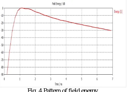
The simulation of time signal has been shown in Fig 3. Here we see that from 0 to 0.4 ns the time signal was 0 but after that time signal increases from 0 to 1 within a short period of time.
Fig. 3 Simulation of time signal
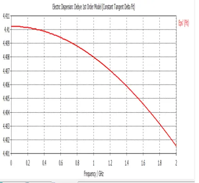
Fig. 5 Change of electric dispersion with frequency
Fig 5 is showing that the change of electric dispersion is consistent with the frequency. With the increase in frequency the electric dispersion is decreasing exponentially.
XVI. CONCLUSION
We have designed a microstrip patch antenna which shows very consistent and better performance. The pattern of field energy, change of electric dispersion with frequency and the return loss shows that our designed microstrip patch antenna shows better performance compared to other microstrip patch antenna.
REFERENCES
[1] M Ozaki, Y. Adachi, Y. Iwahori, and N. Ishii, Application of fuzzy theory to writer recognition of Chinese characters, International Journal of Modelling and Simulation, vol. 18, no. 2, pp. 112-116, 1998
[2] Menzel, W., &Grabherr, W. A microstrip patch antenna with coplanar feed line. IEEE Microwave and Guided Wave Letters, vol. 1, no. 11, pp. 340-342, 1991
[3] Borja, C., Font, G., Blanch, S., &Romeu, J. High directivity fractal boundary microstrip patch antenna. Electronics Letters, vol. 36, no. 9, pp. 778-779, 2000
[4] Yang, K., David, G., Yook, J. G., Papapolymerou, I., Katehi, L. P., & Whitaker, J. F. Electrooptic mapping and finite-element modeling of thenear-field pattern ofa microstrip patch antenna. Microwave Theory and Techniques, IEEE Transactions on, vol. 48, no. 2, pp. 288-294, 2000
[5] Ferrero F., Luxey C., Jacquemod G., &Staraj R. (2005). Dual-band circularly polarized microstrip antenna for satellite applications. Antennas and Wireless Propagation Letters, IEEE, vol. 4, pp. 13-15, 2005