CSEIT1725192 | Received : 08 Oct 2017 | Accepted : 23 Oct 2017 | September-October-2017 [(2)5: 831-836]
International Journal of Scientific Research in Computer Science, Engineering and Information Technology © 2017 IJSRCSEIT | Volume 2 | Issue 5 | ISSN : 2456-3307
831
Design and Implementation of Modified Vedic Multiplier in
FPGA Design Using Zero Knowledge Verification Key
D. Indhu
1, Prof. S. Kamatchi
2 1PG Student, Akshaya College of Engineering and Technology, Coimbatore, Tamil Nadu, India 2Assistant professor, Akshaya College of Engineering and Technology, Coimbatore, Tamil Nadu, India
ABSTRACT
Watermarking as a novel intellectual property protection technique, here the 16Bit Vedic Multiplier is used and it is designed by using AHL circuit and Razor Flip-flop for reducing delay of operation. This modified Vedic multiplier is implemented in FPGA (Xilinx Vertex - 5 Board). With the use of Zero knowledge verification protocol, the FPGA’s Intellectual Property are protect from infringement. This project proposes a new watermarking detection technique based on chaos-based zero-knowledge interaction with Digital signature. The digital signature is watermarked and it is used as a verification key. This digital signature is retrieved by zero knowledge verification protocol. The zero knowledge algorithms is a cryptography based network security algorithm. This protocol is used to resist the sensitive information leakage and embedding attack and is thus robust to the cheating from the prover, verifier, or third party. The result may get better robustness than the most recent related literature.
Keywords: Vedic Multiplier; Watermarking; Zero Knowledge Algorithm; FPGA,AHL, Razor Flipflop;
I.
INTRODUCTION
The modular designed Intellectual Property (IP) cores are easy to be copied or sold by third parties, which results in huge economic losses to IP owners and reduces the market share of their products. Therefore, how to prevent the IP infringement effectively has become a huge challenge for field-programmable gate array (FPGA) vendors and IC designers. Current FPGA IP protection techniques can be roughly classed into two categories, Active techniques devote to binding IPs on specific FPGA platforms to prevent Infringement. Passive techniques mainly include bit stream encryption schemes and digital signature Schemes. Here the 16Bit Vedic Multiplier are design and implement by FPGA and it is watermark for un-trusted buyers by using Zero knowledge verification Protocol. With the prevalence of reusable design methodology in the IC design field, intellectual property (IP) infringement becomes increasingly serious. Multipliers are essential in implementation of systems realizing many important functions such as fast Fourier transforms and multiply accumulate. Multiplier is one of the key hardware blocks in designing arithmetic operation, signal and image processors.
Furthermore, the FPGA IP is essentially a bitstream file. Here the 16-bit Vedic multiplier is designed to take two 16-bit inputs, and arranged each 16-bit input into two 8-bit blocks apply vertically and crosswise method on these blocks and arranged the partial products in a manner so they can be added using carry save adder. The embedded watermark or fingerprint in this file could be tampered with and covered more easily compared with ASIC. Public verification is a huge challenge in the field of FPGA IP watermarking, it is also one of the main obstacles to its application.
II.
RELATED WORK
Zero knowledge protocol
To prevent the leakage of sensitive information, proposed to enhance the robustness of watermarking using a large number of small watermarks instead of one large watermark. However, this method will leak a part of the set of watermarking positions after public verification. When infringement occurs repeatedly, more and more watermarking positions will be given away, which facilitates the attacker to remove more watermarks. It proposed a publicly detectable VLSI watermarking technique that embeds an independent public watermark for public verification. However, this method is not suitable for FPGA designs because public watermarking positions will be leaked after public verification, hence attackers can tamper, remove, or cover the public watermark in the bit stream of FPGA design, which would result in the wrong verification of IP. Zhang et al. [10] proposed a zero-overhead watermarking technique that can resist the removing attack, but as with the methods proposed in [8] and [11], the content and embedded positions would be given away after public verification, bringing a serious threat to watermarking techniques. Zero-knowledge watermarking detection is a method that utilizes zero knowledge and proof of knowledge in cryptography to make the verifier convince the existence of watermarking without leaking sensitive information. Recently, a zero-knowledge-based FPGA digital signature verification scheme was proposed, which addressed the security problem of leaking sensitive information in the public verification. However, it is vulnerable to the following attack: the dishonest IP buyers embed their own watermarks into IP illegally with the same watermarking embedding
algorithm and will not influence the normal function of IP.
Vedic Multiplier
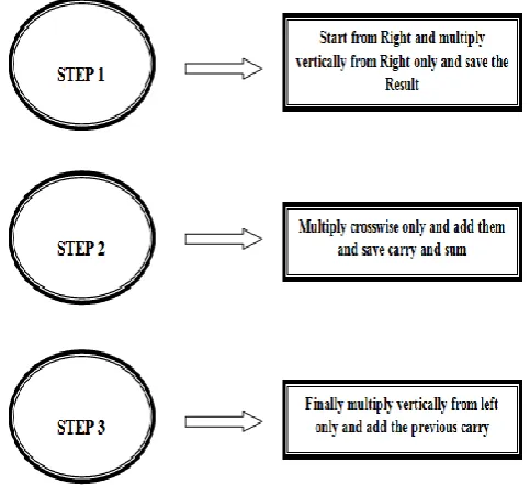
Vedic multiplier is based on Vedic mathematics. In this paper describes the design and FPGA implementation of 16-bit Vedic multiplier. This is designed to take two 16-bit inputs, and arranged each 16-bit input into two 8-bit blocks apply vertically and crosswise method on these blocks and arranged the partial products in a manner so they can be added using adder.
Figure 1. Steps for Vedic multiplier
This based on the “Urdhv Tiryakbhyam” sutra (algorithm). These Sutras have been traditionally used for the multiplication of two numbers in the decimal number system.
Watermarking Scheme
Step 1: In watermarking generation, First the signature S is encrypted with an encryption algorithm. Second, the encrypted S is imputed into a one-way Hash function to generate an abstract ˆS with fixed length. Finally, the watermark W is obtained by scrambling ˆS with hashed chaotic sequence (the initial value of the chaos is used as the key K1).
Step 2: Locating watermark positions: Using a pseudorandom number generator (such as chaos K2 as the key) to generate a pseudorandom sequence as the watermark embedding positions.
Step 4: The input and output of watermarked LUTs are connected with the “do not care” inputs of the original circuit in order to disguise the embedded watermark.
chaos based zero knowledge verification protocol
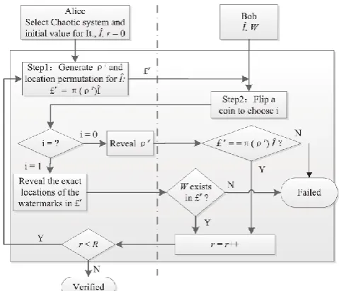
A. Protocol Overview
Zero-knowledge public verification is to prove that the watermark of IP owner exists in the bit stream of FPGA design without revealing the watermarking content and position. Assume the prover is Alice and the verifier is Bob. According to the watermark generation and embedding algorithm, Alice gets W
based on S. Then W is embedded into I (FPGA design) to get ˆ I. Alice wants to prove the existence of W
without leaking its position. The process of zero-knowledge verification protocol is shown in Fig.2. The steps of zero-knowledge watermarking verification protocol are as follows.
Step 1: Alice generates a random chaotic sequence x
(chaotic initial value as the key). x is binarized into the two- value chaotic sequence ρ. ρ is used as the input of position permutation algorithm π(ρ).
π(ρ) is applied to ˆ I for random position permutation, that is, ξ = π(ρ) ˆ I, then send ξ to Bob
Step 2: Bob knows ˆ I and ξ, then flips coin i to decide that either Step 2a or Step 2b should be executed by
Alice.
Figure 2. Zero-knowledge verification protocol between prover Alice and verifier Bob.
Step 2a: Reveal ρ.
Step 2b: Reveal watermarking positions in ξ.
Step 3: If i = 0, Alice executes Step 2a; if i=1, Alice executes Step 2b.
Step 4: Bob executes Step 4a if Step 2a is executed, or executes Step 4b if Step2b is executed.
Step 4a: Confirm that ξ is a legal permutation for
ˆ I, that is, ξ = π(ρ) ˆ I .
Step 4b: Verify whether W exists in ξ.
Step 5: Discard the chaotic sequence ρ.
Steps 1-5 are executed R rounds. Each round will generate a new chaotic sequence for random position permutation. In order to reduce the probability that Alice succeeded in deceiving Bob, Steps 1-5 must be executed R rounds. If R rounds are passed, the embedded watermark can be verified without revealing sensitive information. In addition, we can prevent the leakage of watermarking content by encoding the LUT content of ˆ I . How to encode securely and efficiently is not the focus of this paper. There are many mature coding methods that have been proposed, such as linear feedback shift register and nonlinear feedback shift register. It is worth noting that the proposed verification scheme is also suitable for other FPGA IP watermark methods. In this paper, we use the hashed chaotic sequence to scramble the watermark to enhance the robustness.
B. Protocol Implementation
π(ρ) is applied to ˆ I to get ξ. The implementation of protocol is described in detail as follows.
Generation of two-value chaotic sequences
1-D discrete chaotic map f : U →U,U ⊂R
xk+1 = f (xk, λ), xk ∈U, λ ∈R (1)
where K represents the number of iterations and λ is a parameter to control the behavior of chaotic system. For a specific λ, the finite set U is composed of periodic sequences and chaotic sequences. Selecting the λ properly, x will be able to form a chaotic sequence. Logistic mapping is a kind of widely researched dynamical system. The definition is as follows:
xk+1 = μxk(1 − xk ) (2)
where μ ∈ [0, 4], xk ∈(0, 1). When 3.5699456 < μ_4, Logistic mapping works in chaotic state. The chaotic sequence generated by x0 is periodic, non-convergent, and very sensitive to the initial value. For example, the form of logistic mapping defined at the interval (−1, 1) is as follows:
xk+1 = 1 − μx2k (3)
The probability density function of the chaotic sequences generated when parameter μ = 2 is as follows:
ρ(x) =1/ π √1 + x2, −1 < x < 1 0, else (4) where π denotes pi. Equation (4) can deduce two import statistical properties of the chaotic sequences, the mean value of trajectory points and the cross correlation between chaotic sequences. The mean value of trajectory points of chaotic sequences is as follows:
(5) Selecting two initial values x0 and y0, we get the cross correlation between chaotic sequences
(6) Real chaotic sequences generated by formula (2) can be represented by the binary system
x = 0.b1(x)b2(x) . . . bi (x) . . . , x ∈ [0, 1], bi (x) ∈ 0, 1.
(7) The bi (x) shows as
(8) where Ɵt (x) is the threshold function, shown as
Ɵt (x) = {0, x < t
{1, x>t. (9) A two-value chaotic sequence can be obtained after binarization
ρn
i={bi(τn(x))}∞n=0 (10)
where n is the length of the sequence and τ n(x) denotes
n-time iterations of logistic mapping. It is worth noting that the two value chaotic sequence has good autocorrelation and cross correlation properties. ρn i
plays an important role in the random position permutation algorithm and is used to control whether the position permutation of LUTs should be executed.
III.
PROTOCOL ANALYSIS
A. Analysis of Protocol Properties
The zero-knowledge protocol should satisfy three properties: completeness, soundness, and zero-knowledge. We will discuss these properties in detail.
1) Completeness: In each round of verification, the verifier flips a coin to decide either Step 2a or Step 2b to be executed by Alice. Step 2a or Step 2b will not give away the true positions of the watermark in ˆ I
(provided that Step2a and Step2b are not executed at the same time). In the case of the protocol being executed for many rounds, the verifier always accepts the proof of the prover if Alice can prove Step 2a or Step 2b. Therefore, an honest prover can always make the verifier believe that he does embed the watermark into the FPGA IP. The protocol is complete.
successfully with the probability 1/2. When the protocol iterates R times, the above probability would be 1/2R. Hence, the reliability of protocol is S = 1 − 1/2R. When R is large enough, S approaches 1. Therefore, the possibility can be ignored that a dishonest prover can make the verifier believe that he embeds a legal watermark in the FPGA design. The protocol is sound.
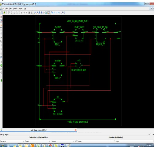
Design of 16-Bit Vedic multiplier
16bit Vedic multiplier is designed to take two 16-bit inputs, and arranged each 16-bit input into two 16-bit blocks apply vertically and crosswise method on these blocks and arranged the partial products in a manner so they can be added using carry save adder. This based on the “Urdhv Tiryakbhyam” sutra (algorithm). These Sutras have been traditionally used for the multiplication of two numbers in the decimal number system.
Figure 3. RTL block for 16 Bit Vedic multiplier
IV.
PROPOSED METHOD
The modular designed Intellectual Property (IP) cores are easy to be copied or sold by third parties, which results in huge economic losses to IP owners and reduces the market share of their products. Therefore, how to prevent the IP infringement effectively has become a huge challenge for field-programmable gate array (FPGA) vendors and IC designers. Watermarking as a novel intellectual property (IP) protection technique, here the Vedic Multiplier is used. It can protect FPGA’s Intellectual Property from infringement. Here the 16Bit Vedic Multiplier are designed and
implemented in FPGA. This project proposes a new watermarking detection technique based on chaos-based zero-knowledge interaction with Digital signature. Used to resist the sensitive information leakage and embedding attack and is thus robust to the cheating from the prover, verifier, or third party. 16-bit Vedic multiplier is designed to take two 16-bit inputs, and arranged each 32-bit input into two 8-bit blocks apply vertically and crosswise method on these blocks and arranged the partial products in a manner so they can be added using carry save adder. This Vedic Multiplier designed and it is implemented in a FPGA (Xilinx vertex - V Board). The modified 16 bit Vedic multiplier is designed with AHL circuit and Razor Flip-flop.
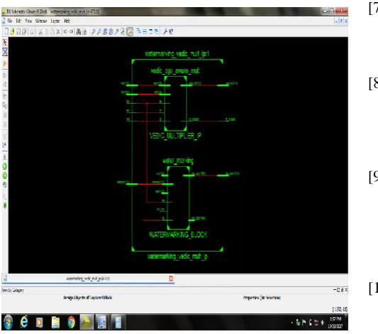
Figure 4. Block Diagram for Proposed system
The digital signature is watermarked and it is used as a verification key. By using digital signature (pass word) the Vedic multiplier is protect from the attacker or third party. The zero knowledge verification protocol is used to protect the IP from un-trusted buyers or verifiers.
V.
CONCLUSION AND FUTURE SCOPE
permutation in the zero-knowledge protocol, the proposed scheme has high position permutation robustness. In future work encryption and decryption algorithm should be modified for its efficiency.
VI.
RESULT
Thus the design and implementation of modified Vedic multiplier is designed and implemented in FPGA (Xilinx Virtex-V Board) Design. This modified Vedic multiplier is designed by using AHL circuit and Razor Flipflop for reducing the delay.
Figure 5. Output for proposed system
This efficient Vedic multiplier is protected by watermarked digital signature (verification key) by using chaos based zero knowledge verification protocol. This overall function was done in Xilinx ISE 14.2 suite.
VII.
REFERENCES
[1] Jiliang Zhang and Lele Liu, “ Publicly Verifiable Watermarking for Intellectual Property Protection in FPGA Design” Vol 25 | Issue 4, April 2017 IEEE (pp.1520-1527).
[2] J. Zhang, Y. Lin, Q. Wu, and W. Che, “Watermarking FPGA bit file for intellectual property protection”, Radio engineering, vol. 21, no. 2,pp. 764-771, Jun. 2012.
[3] Saha, P., Banerjee, A., Bhattacharyya, P., and Dandapat, A. ”High speed ASIC design of complex multiplier using vedic mathematics”. In Students Technology Symposium, Jan. 2011 IEEE (pp. 237-241).
[4] Anuva Das, Mrs.J.K.Kasthuri Bhai, “Design Optimization of Vedic Multiplier using Reversible Logic” International Journal of Engineering Research & Technology (IJERT), Vol. 3 Issue 3, March 2014, ISSN: 2278-0181. [5] Vaijyanath Kunchigi, Linganagouda Kulkarni,
SubhashKulkarni, “High Speed and Area Efficient Vedic Multiplier”, IEEE, Devices, Circuits and systems,Vol.4,pp.360-364,15-16 March 2012.
[6] Sudeep.M.C, SharathBimba.M, “Design and FPGA Implementation of High Speed Vedic Multiplier”, International Journal of Computer Applications, Vol. 90, Issue 16, March 2014. [7] M.A. Gora, A. Maiti and Schaumont, “A Flexible
design flow for software IP binding in FPGA,” IEEE Trans. Ind Informat, vol.6, no. 4, pp.719-728, Nov. 2010.
[8] D.Saha and S.Sur-Kolay, “ Secure public verification of IP marks in FPGA design through a zero knowledge protocol,” IEEE Trans. Very Large Scale Integr. (VLSI) Syst, vol. 20, no.10, pp. 1749-1757. Oct. 2012.
[9] Gupta.A, Malviya.U, Kapse. V, “A Novel Approach To Design A High Speed Arithmetic Logic Unit Based on Ancient Vedic Multiplier Technique”, International Journal of Modern Engineering Research (IJMER), Vol. 2, Issue4, pp. 2695-2698, July-Aug 2012.
[10] Ramachandran S, Pande K.S, “Design, Implementation and Performance Analysis of an Integrated Vedic Multiplier Architecture”, International Journal of Computational Engineering Research, Vol.2 Issue3, pp. 697-703, May-June 2012.
[11] J.Kufel, P.R Wilson, S. Hill, B.M.AI-Hashimi, and P.N.Whatmough, “Sequence-aware watermark design for soft IP embedded processors”, IEEE Trans. Very Large Scale Integr. (VLSI) Syst, vol. 24, no.1, pp. 276-289, Jan. 2016.