CSEIT1833534 | Received:25 March 2018| Accepted:10 April 2018 | March-April-2018 [(3)4: 1104-1110]
International Journal of Scientific Research in Computer Science, Engineering and Information Technology © 2018 IJSRCSEIT | Volume 3 | Issue 4| ISSN: 2456-3307
1104
Single Ended 9T Subthreshold SRAM Cell For Low Power
Applications Using Dynamic Feedback Control
M. Vijaykanth
1, N. Nagaraju
21M.Tech Student, Department Of ECE, RGM Engineering College,Kurnool, Andhra Pradesh, India 2Associate Professor, Department Of ECE, RGM Engineering College, Kurnool, Andhra Pradesh, India
ABSTRACT
A single-ended nine transistor (9T) Static Random Memory (SRAM) cell is presented in this paper which improves read stability and write ability. The cell employs separate access transistors for read and write operations to eliminate the conflicting design requirement on access transistors. The cell employs feedback loop cut off scheme along with power supply interuption scheme to enhance the write ability. Simulation is done on 180nm standard CMOS technology on Tanner EDA. The proposed single-ended with dynamic feedback control 9T static RAM (SRAM) cell enhances the static noise margin (SNM) for ultralow power supply. Simulation results show that read SNM (RSNM) and write SNM (WSNM) of the proposed cell are 2.77x and 1.12x larger respectively, than those of conventional 8T cell at 1V. Proposed cell consumes 1.4x lesser leakage power than the conventional 8Tcell.
Keywords : Single ended, static noise margin (SNM), static RAM (SRAM), subthreshold, ultralow power.
I.
INTRODUCTION
The portable microprocessor controlled devices contain embedded memory, which represents a large portion of the system-on chip (SoC). These portable systems need ultralow power consuming circuits to utilize battery for longer duration. The power consumption can be minimized using nonconventional device structures, new circuit topologies, and optimizing the architecture. Although, voltage scaling has led to circuit operation in subthreshold regime with minimum power consumption, but there is a disadvantage of exponential reduction in performance. The circuit operation in the subthreshold regime has paved path toward ultralow power embedded memories, mainly static RAMs (SRAMs). However, in subthreshold regime, the data stability of SRAM cell is a severe problem and worsens with the scaling of MOSFET to sub nanometer technology. Due to these limitations it becomes difficult to operate the conventional 6-transistor (6T) cell at ultralow voltage (ULV) power supply. In addition, 6T has a severe problem of read disturb. The
basic and an effective way to eliminate this problem is the decoupling of true storing node from the bit lines during the read operation. This read decoupling approach is utilized by conventional 8-transistor [read decoupled 8-transistor (RD-8T)] cell which offers read static noise margin (RSNM) comparable with hold static noise margin (HSNM). However, RD-8T suffers from leakage introduced in read path. This leakage current increases with the scaling thereby, increasing the probability of failed read/write operations. Similar cells that maintain the cell current without disturbing the storage node are also proposed.
ended 5T severely degrades in comparison with conventional 6T SRAM cell. Various approaches like boosted supply (gate voltage of access transistor M5 is greater than VDD) generated from an additional circuit, gated-feedback write assist, 7T dual VTH , asymmetrical write/read-assist 8T, and cross-point data-aware 9T have been proposed to mitigate the above issues associated with 5T. Still, none of the cell could fulfill the requirement of improving both read and write stability in subthreshold regime for ultralow power applications.
II.
PREVIOUS WORK
1. Conventional 6T SRAM:
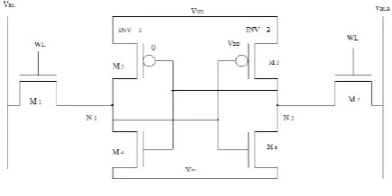
SRAM bitcell is the basic building block of SRAM caches. Each bitcell stores one bit of information. The main parameters that should keep in mind while designing SRAM bitcells are bitcell area, speed, stability, power consumption and yield. Fig. 1 shows the schematic diagram of conventional 6T SRAM bitcell. A conventional 6T-SRAM bitcell consists of two cross coupled inverters (INV1 and INV2) and access transistors (M1 and M2). The access transistors allow access to the data stored during read and write operations and provide isolation from other bitcells during hold state. Bitcells are accessed by asserting the word-line (WL) during a read or write operation by the access transistors.
Figure 1. Schematic diagram of a standard 6T SRAM bit cell
A. Read operation
Fig. 2 shows the 6T SRAM equivalent schematic diagram during read operation. Bit lines are precharged to supply voltage before read operation. The read operation is initiated by enabling the word-line (WL) and thereby connecting the internal nodes of the SRAM bitcell to bit-lines. The bit line voltage is pulled down by the nMOS transistor at the „0‟ storage node and the
difference between two bit line voltages will be detected by sense amplifier. When the word line (WL) is high, one of the bit line voltages is pulled down through transistors M2 and M6 or M1 and M4. The transistors M2 and M6 forms a voltage divider, because of current flowing through M2, the potential at node QB is no longer at „0‟V. Also it should not go beyond switching threshold of inverter (INV1) to avoid destructive read. The rising of potential depends on sizing of access transistor and pull down transistor which is defined as a bitcell ratio.
Figure 2. Read equivalent diagram of a standard 6T SRAM bitcell
B. Write operation
The write operation begins by forcing a differential voltage (VDD, and 0) at the bitline pairs (BLB and BL). This differential voltage corresponds to the data to be written at the storage nodes (Q and QB) and it is controlled by the write drivers. The WL is then activated to store the information from the bit-line pairs to corresponding storage nodes. Assume, the nodes Q and QB initially store values „1‟ and „0‟ respectively. When the WL is asserted the access transistor (M1) connected to BL (at „0‟) is turned on, a current flows from VDD to BL through M3 and M1. This current flow lowers the potential at Q. The potential at the node Q has to go below the trip point of the inverter (INV2) for a successful write operation and this depends on the ratio of pull-up transistor (M3) and the access transistor (M1). This ratio is referred to as the pull-up - ratio.
C. Hold operation
capacitance) will increase which are desirable. However, at the same time power consumption and write time increases which are not desirable features, as they incur loss of power, performance and increase in area overhead.
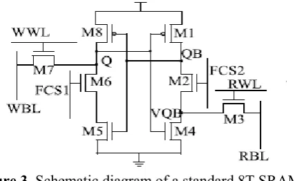
2. 8T SRAM Cell Design
To make a cell stable in all operations, single-ended with dynamic feedback control (SE-DFC) cell is presented in Fig. 3. The single-ended design is used to reduce the differential switching power during read– write operation. The power consumed during switching/ toggling of data on single bit line is lesser than that on differential bit-line pair. The SE-DFC enables writing through single nMOS in 8T. It also separates the read and write path and exhibits read decoupling. The structural change of cell is considered to enhance the immunity against the process–voltage– temperature (PVT) variations. It improves the static noise margin (SNM) of 8T cell in subthreshold/near-hold mode. The write word line (WWL) controls only one nMOS transistor M7, used to transfer the data from single write bit line (WBL). A separate read bit line (RBL) is used to transfer the data from cell to the output when read word line (RWL) is activated. Two columns biased feedback control signals: FCS1 and FCS2 lines are used to control the feedback cutting transistors: M6 and M2, respectively.
Figure 3. Schematic diagram of a standard 8T SRAM bit cell
A. Write Operation
The feedback cutting scheme is used to write into 8T. In this scheme, during write 1 operation FCS1 is made
low which switches OFF M6. When the RWL is made low and FCS2 high, M2 conducts connecting Complementary Q (QB) to the ground. Now, if the data applied to word bit line (WBL) is 1 and WWL is activated (Table II), then current flows from WBL to Q
and creates a voltage hike on Q via M7-writing 1 into the cell. Moreover, when Q changes its state from 0 to 1, the inverter (M1– M2–M4) changes the state of QB from 1 to 0. To write a 0 at Q, WWL is made high, FCS2 low and WBL is pulled to the ground. The low going FCS2 leaves QB floating, which can go to a small negative value, and then the current from pull-up pMOS M1 charges QB to 1. The WT is measured as the time taken by WWL signal-to-rise to VDD/2 until the storage nodes intersect each other. The simulations for WT were performed at all process corners. The WT (for write 1 and write 0) for 8T increases (Fig. 4) with the decrease in power supply. The WT is highest for slown MOS and slow pMOS (SS) worst case corner, as shown in Fig. 4(a) and (b). During write 1/0 operation, the power consumption of 8T is highest for fast nMOS and fast pMOS (FF) process corner dominated by the fast switching activities (Fig. 5). As write 0 operation is faster than write 1, the write 0 power consumption during write 0 is more as compared with that of write 1
WWL, FCS1, and FCS2 were made low during the read operation (Table II), therefore, there is no direct disturbance on true storing node QB during reading the cell. The low going FCS2 leaves QB floating, which goes to a negative value then comes back to its original 0 value after successful read operation. If Q is high then, the size ratio of M3 and M4 will govern the read current and the voltage difference on RBL. During read 0 operation, Q is 0 and RBL holds precharged high value and the inverter sense amplifier gives 0 at output. Since M2 is OFF so virtual QB (VQB) is isolated from QB and this prevents the chance of disturbance in QB node voltage which ultimately reduces the read failure probability and improves the RSNM. During read operation, if FCS1/FCS2 turns 1 before RWL is turned 0 then QB and VQB can share charge. As WWL is 0 no strong path exists between WBL and Q, and any disturbance in QB will not affect Q. After that if RWL goes low, the positive feedback will restore the respective states (Q = 1 and QB = 0).
The read time is measured as the time the RWL signal is activated until the RBL is discharged to 90%. The SS process corner shows maximum read time, as shown in Fig. 6(a). It is followed by the SF corner and then by the other process corners. Similar to write power, the FF process corner condition draws the highest read power. While read power consumption at other process corners closely follows for different power supplies.
Figure 6. (a) Read 1 time. (b) Read 1 power of 8T.
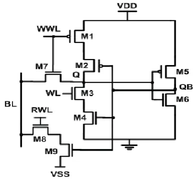
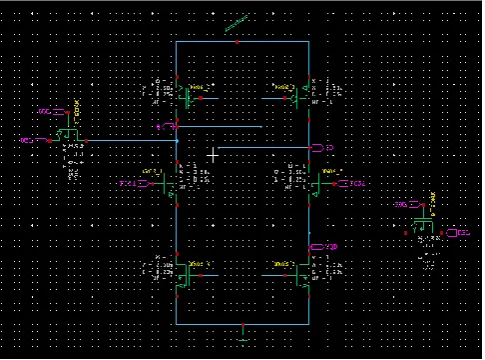
III. PROPOSED SINGLE ENDED 9T CELL
The schematic of proposed 9T cell is depicted in Fig. 7. Truth Table of the proposed cell is given. Transistors M2- M4 form left inverter while the right inverter is formed by transistors M5- M6. Transistors M1 is used to make transistor M2 weaker during write „0‟ operation, while transistor M3 is turned OFF to perform successful write „1‟ operation. M7 is write access transistor controlled by Write Word Line (WWL) for writing data from bit line BL in to the storage node
Q. Transistors M8 and M9 form a separate read buffer for read operation. In the hold mode, WWL and Read word line (RWL) are forced to logic „0‟ while WL and VSS are forced to VDD. The cell retains the stored bit as long as power supply is ON.
Figure 7. Proposed 9T SRAM cell
To read the content of the cell, bit line BL is precharged to VDD and RWL is enabled to turn ON transistor M8. Control signal WL is raised to VDD while VSS and WWL are pulled down to ground. Now, if „0‟ is stored in the cell (Q = ‟0‟, QB = „1‟) then, M9 turns ON and BL is discharged to ground through M8 and M9. If „1‟ is stored in the cell (Q= „1‟, QB=„0‟) then, M9 is OFF and BL remains at its precharged value. The write operation is performed by raising WWL, WL and to VDD and lowering RWL to ground. For writing a „0‟ in the cell, BL is loaded with data „0‟. High WWL turns ON M7 to discharge node Q to the ground. To write a „1‟ in the cell WWL is forced to VDD while WL and RWL are pulled to ground. Low WL disables the transistor M3 which disconnects the storage node Q from ground during write „1‟ mode. Now, data „1‟ is applied to BL which causes current to flow from BL to node Q through M7. As a result, the voltage at node Q is raised which switches ON M6. Consequently, QB is pulled down to ground through M6 and finally „1‟ is written into the cell. After successful write operation, the cell goes into hold mode by raising WL to VDD and lowering WWL to ground.
A. Read Stability
read operation at VDD = 400mV. RSNM is measured as the side length of the largest square embedded inside the butterfly curves formed by the read VTCs. In the proposed design, read current does not flow through the storage node and therefore voltage at „0‟ storing node does not rise above the ground), hence, proposed 9T cell exhibits RSNM equal to that of HSNM. From the Fig. 5, it is noticed that the proposed cell offers 2.77x larger RSNM than that of the conventional 6T cell at Vdd = 400mV. Fig.9 shows the RSNM as a function of the supply voltage for proposed 9T and the conventional 6T cell.
Figure 8. Read butterfly curves
Figure 9. RSNM versus Supply Voltage
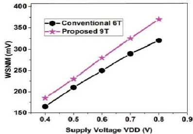
B. Write Stability
Write stability is expressed in terms of WSNM. During write operation, OFF transistors M1 and M3 disconnect the storage node Q from VDD and ground. Therefore, the cell achieves enhanced write ability compared to the 6T cell. Fig. 10 shows the WSNM versus VDD curves for proposed and the conventional 6T cells. From Fig. 8, it is noticed that 9T cell offers 1.12x larger WSNM as compared to the conventional 6T cell at 1 V.
Figure 10. WSNM versus Power Supply
C. Hold Stability
Hold SNM measures the cell stability when the cell is in standby mode. During hold state, 9T cell behaves like the conventional 6T cell therefore, HSNM of the proposed cell is almost equal to that of the conventional 6T cell.
IV. RESULTS
Figure 11. 9T SRAM
Figure 13. 8T SRAM
Figure 14. Waveforms
Table 1: Comparison table
6T 8T Proposed 9T
Area (T) 6 8 9
Delay (ns) 9.9678 9.9769 12.961
Power(mw) 0.677 0.454 0.014
V. CONCLUSION
A 9T SRAM cell with enhanced write ability has been presented in this paper. Use of separate read and write ports eliminates the read versus write design conflict. The cell also eliminates the read disturb problem by employing separate read buffer. The proposed cell offers 1.12x larger WSNM and 2.77x larger RSNM
compared to that of the conventional 6T and 8T cell at 1V. We attained enhanced SNM in subthreshold regime using SE-DFC and read decoupling schemes. The proposed cell‟s area is twice as that of 6T. The cell consumes lower switching power due to use of single bit line. Our cell dissipates 0.98x lesser leakage power than that of conventional 6T and 8T cell at 1.0 V. The advantage of reduced power consumption of the proposed 9T cell enables it to be employed for battery operated SoC design. Future and applications of the proposed 9T cell can potentially be in low/ULV and medium frequency operation like neural signal processor, subthreshold processor.
VI. REFERENCES
[1]. K. Roy and S. Prasad, Low-Power CMOS VLSI Circuit Design, 1st ed. New York, NY, USA: Wiley, 2000.
[2]. N. Verma and A. P. Chandrakasan, “A 256 kb 65 nm 8T subthreshold SRAM employing sense-amplifier redundancy,” IEEE J. Solid-State Circuits, vol. 43, no. 1, pp. 141–149, Jan. 2008. [3]. C. Kushwah and S. K. Vishvakarma, “Ultra-low
power sub-threshold SRAM cell design to improve read static noise margin,” in Progress in VLSI Design and Test (Lecture Notes in Computer Science), vol. 7373. Berlin, Germany: Springer-Verlag, 2012, pp. 139–146.
[4]. B. H. Calhoun and A. P. Chandrakasan, “A 256-kb 65-nm sub-threshold SRAM design for ultra-low-voltage operation,” IEEE J. Solid-State Circuits, vol. 42, no. 3, pp. 680–688, Mar. 2007. [5]. C. B. Kushwah, D. Dwivedi, and N. Sathisha,
“8T based SRAM cell and related method,” U.S. Patent IN920130 218 US1, May 30, 2013. [6]. J. P. Kulkarni, K. Kim, and K. Roy, “A 160 mV
robust Schmitt trigger based subthreshold SRAM,” IEEE J. Solid-State Circuits, vol. 42, no. 10, pp. 2303–2313, Oct. 2007.
[7]. C.-H. Lo and S.-Y. Huang, “P-P-N based 10T SRAM cell for low leakage and resilient subthreshold operation,” IEEE J. Solid-State Circuits, vol. 46, no. 3, pp. 695–704, Mar. 2011. [8]. I. Carlson, S. Andersson, S. Natarajan, and A.
Alvandpour, “A high density, low leakage, 5T SRAM for embedded caches,” in Proc. 30th Eur. Solid-State Circuits Conf., Sep. 2004, pp. 215– 218.
subthreshold SRAM,” IEEE J. Solid-State Circuits, vol. 43, no. 10, pp. 2338–2348, Oct. 2008.
[10]. S. A. Tawfik and V. Kursun, “Low power and robust 7T dual-Vt SRAM circuit,” in Proc. IEEE Int. Symp. Circuits Syst., May 2008, pp. 1452– 1455.
[11]. Ming-Hsien Tu et al., "A single -ended disturb-free 9T sub-threshold SRAM with cross-point data-aware write word-line structure, negative bit-line and adaptive read operation timing tracing, "IEEE J. Solid state circuits, vol. 47, no. 6, pp. 1469-1482, June 2012.
[12]. C. Y. Lu et al., “A 0.325 V, 600-kHz, 40-nm 72-kb 9T subthreshold SRAM with aligned boosted write word line and negative write bit line write-assist,” IEEE Trans. Very Large Scale Integr. (VLSI) Syst.,vol. 23, no. 5, pp. 958–962, May 2015
[13]. E. Seevinck, F. J. List and J. Lohstroh, “Static noise margin analysis of MOS SRAM cells, "IEEE J. Solid -State Circuits, vol.22, no. 5, pp. 748-754, Oct. 1987.
[14]. J. P. Kulkarni, K. Kim, and K. Roy.," A 160 mV robust Schmitt trigger based sub-threshold SRAM," IEEE J. Solid state circuit circuits, vol.42, no.10, pp. 2303-2313 Oct 2007.
[15]. S. Ahmad et al., "Single ended Schmitt-trigger based robust low power SRAM cell," IEEE trans. very large scale integration (VLSI) system, vol. 24, no.8, pp. 2634-2642, Aug. 2016.
[16]. G. Pasandi, and S. M. Fakhraie, “A 256-kb 9T near-threshold SRAM with 1k cells per bitline and enhanced write and read operations,” IEEE trans IEEE Trans. Very Large Scale Integr. (VLSI) Syst, vol. 23, no.11, pp. 2438-2446, Nov 2015.