ANALYSIS AND DESIGN OF ALL-OPTICAL
SWITCHING IN APODIZED AND CHIRPED BRAGG GRATINGS
M. J. Moghimi andH. Ghafoori-Fard
Faculty of Electrical Engineering Amirkabir University of Technology Tehran, Iran
A. Rostami
Photonics and Nanocrystal Research Laboratory Faculty of Electrical and Computer Engineering University of Tabriz
Tabriz 51664, Iran
Abstract—In this paper, effects of the different apodization and chirp
functions in one-dimensional nonlinear Bragg grating on switching characteristics are studied. It is shown that with increasing the Gaussian width in the case of Gaussian apodization, slope of transfer function is increased. The situation is same in the case of raised cosine apodization function too. Also, in the case of quadratic apodization with decreasing the apodization parameter the slope of the transfer function is improved. Using the chirp different functions the switching threshold can be controlled. So, the presented structure as optical switch can be designed for optimum slope and threshold of switching using desired apodization and chirp functions. So, the presented material in this paper shows that there are possibilities for management of all-optical switching using suitable apodization and chirp functions.
1. INTRODUCTION
packet of wavelengths propagating through optical fiber network. These functions can be realized using passive components, which there are interesting and currently used for optical signal processing. In optical passive devices the Bragg gratings is widely used, discussed in literature and applied for optical signal processing tasks. Usually, these devices can be implemented using Bragg gratings. Nowadays, from our point of view, these functions are implemented separately (single function passive device) without efficient controllable and reconfigurable algorithm in electrical (electro-optical functional blocks) and optical domains (all-optical functional blocks). So, if optical devices can be integrated into electronically controllable geometry there will be a basis for the programmable optical functional devices. These types of devices really are new and useful for more development of optical processing and computing with flexible programming. So, there is basic interest for introducing and development of the mentioned devices and systems for realization of optical computing. In this paper we concentrate on optical switching devices made by Bragg gratings because of important role in optical communication.
for optical switching and they didn’t consider apodization and chirp of refractive index on switching characteristics. So, in this paper we consider this subject and investigate effects of the apodization and chirp of refractive index on optical switching performance. We show that using these factors there are two degree of freedom to manipulate the switching characteristics. Thus optimization in presence of these factors can be done effectively.
Organization of the paper is as follows.
In Section 2 mathematical background for modeling of the light propagation in apodized and chirped periodic media is presented. Simulation result and discussion is presented in Section 3. Finally the paper ends with a short conclusion.
2. MATHEMATICAL BACKGROUND
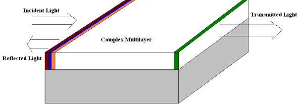
For optical switching the following proposal is considered. In this figure a thick substrate and a thin optical complex multilayer generally including different index of refraction and layer thickness is considered as an optical switch.
Figure 1. Schematic of the proposed optical switch.
For this structure the index of refraction generally can be explained as follows.
n(x)=nave+f(x)
δlsin(kx+Φ(x))−E2δnlsin(kx+Φ(x))
k=2π Λ
(1)
wherenave,δl,δnl, ΛiE,f(x) and Φ(x) are average index of refraction,
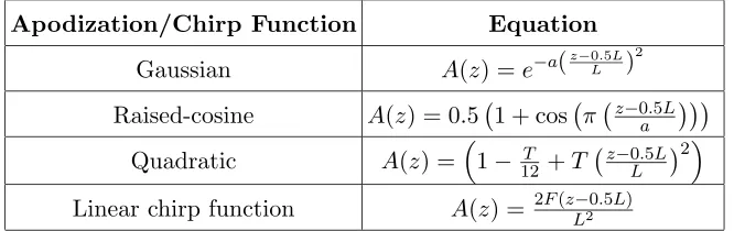
Table 1. List of apodization functions.
Apodization/Chirp Function Equation
Gaussian A(z) =e−a(z−0L.5L) 2
Raised-cosine A(z) = 0.51 + cosπz−0a.5L
Quadratic A(z) =
1−12T +Tz−0L.5L2
Linear chirp function A(z) = 2F(zL−20.5L)
To analyze this structure, we divided it into N sections. Each section is considered homogenous. The approximated multilayer dielectric structure is described by
n(x) =
n0 x < x0
n1 x0 < x < x1
n2 x1 < x < x2 ..
.
nN xN−1 < x < xN
ns xN < x
, (2)
wherenl,xl,nsandn0are the refractive index oflth layer, the position of the interface between the lth layer and the (l+ 1)th layer, the substrate index of refraction and the incident medium refractive index respectively. The layer thickness di is L/N where L is the length of the grating.
di= L
N, i= 1,2,3, . . . , N (3)
The electric field of a general plane-wave solution of the wave equation can be written as:
E =E(x)ei(ωt−βz), (4)
where the electric field distributionE(x) can be written as:
E(x) =
A0e−ik0x(x−x0)+B0eik0x(x−x0) x < x0
Ale−iklx(x−xl)+Bleiklx(x−xl) xl−1 < x < xl Ase−iksx(x−xN)+Bseiksx(x−xN) xN < x
whereklx is the xcomponent of wave vector
klx =
n
lω c
2
−β2
1 2
, (6)
and is related to the ray angleθl by:
klx =nl ω
c cos(θl) =
2π
λ cos(θl) (7)
The electric field E(x) consists of right and left traveling waves and can be defined as follows.
El(x) = Re−iklx+Leiklx=Al(x) +Bl(x), (8)
where±klx,R and L are constants in homogenous layer respectively.
E(x) is a continuous function ofx. If we represent two amplitudes of
E(x) as column vectors, the column vectors are related by:
A0
B0
= D0−1Dl
Al Bl
(9)
Al Bl
= PlDl−1Dl+1
Al+1
Bl+1
, (10)
whereAl,BlandDlrepresent the amplitude of plane waves at interface x=xl and dynamical matrix respectively described by:
Dα=
1 1
nαcosθα −nαcosθα
, α= 0, l, l+ 1 (11)
whereθαandPlare the ray angle in each layer and propagation matrix
respectively and defined by:
Pl =
eiφl 0 0 e−iφl
(12)
φl = klx·dl (13)
The relation between A0, B0 and As, Bs (or AN+1, BN+1) can be determined by:
A0
B0
=
M11 M12
M21 M22
As Bs
(14)
M11 M12
M21 M22
=D0−1
N
i=1
DiPiDi−1
Ds (15)
This approach named Transfer Matrix Method (TMM). If the light is
0 0. 5 1 1. 5 2 2. 5 3 3. 5 4 4. 5 5 × 10⁵ 0
0. 1 0. 2 0. 3 0. 4 0. 5 0. 6 0. 7 0. 8 0. 9 1
Incident Electric Field (V/m)
R
ef
le
cti
o
n
Co
ef
fic
ie
n
t
0. 5mm 0. 4mm 0. 3mm 0. 2mm
(a)
0 0. 2 0. 4 0. 6 0. 8 1 1. 2 1. 4 1. 6 1. 8 2 × 10⁶ 0
0. 1 0. 2 0. 3 0. 4 0. 5 0. 6 0. 7 0. 8 0. 9 1
Length (nm)
A
p
o
d
iz
at
ion
Func
ti
on
0. 5mm 0. 4mm 0. 3mm 0. 2mm
(b)
Figure 2. (a) The reflection coefficient vs. incident electric field
incident from medium 0, the reflection coefficient is defined as:
r(λ) =
B0
A0
Bs=0
(16)
Similarly, the transmission coefficient is:
t(λ) =
As A0
Bs=0
(17)
Using matrix Equation (14) and definitions (15), (16), we obtain:
r(λ) = M21
M11
(18)
and
t(λ) = 1
M11
(19)
Reflectance is given by:
R(λ) =|r(λ)|2 =M21
M11
2 (20)
Provided medium 0 is lossless.
3. SIMULATION RESULTS AND DISCUSSION
In this section simulated results for the proposed structure are illustrated and discussed. In the following first we consider effects of different apodization functions on switching characteristics and then we study effect of the chirp function.
3.1. Gaussian Apodization Function
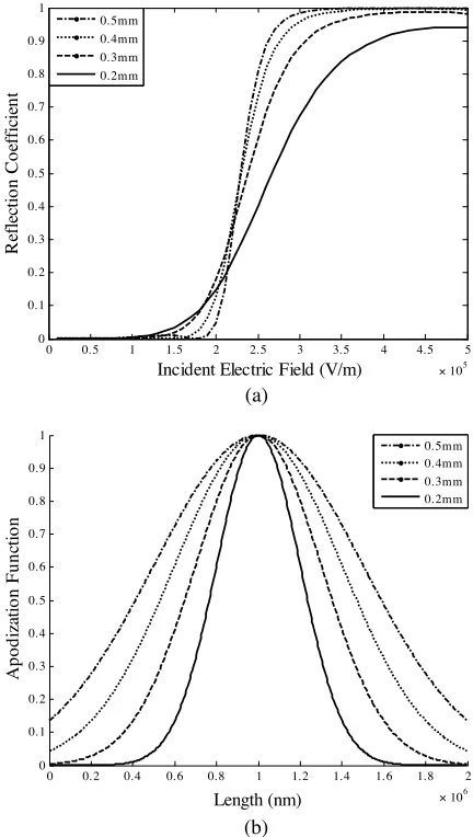
In this case the Gaussian apodization profile is assumed as follows.
A(z) =e
−a(z−0.5L L )
2
, (21)
whereais the Gaussian width. For this apodization function and given constant the reflection coefficient and functions are shown in Fig. 2.
3.2. Raised-cosine Apodization Function
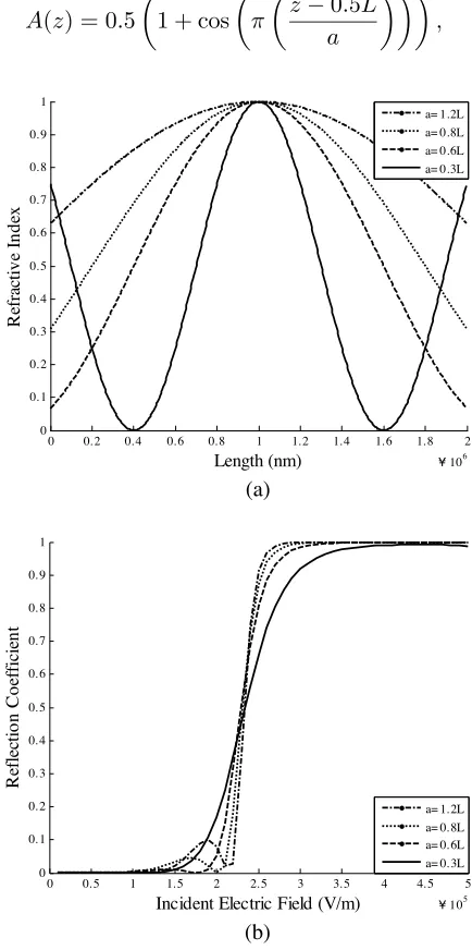
For this case the following apodization function is adopted.
A(z) = 0.5
1 + cos
π
z−0.5L a
, (22)
0 0. 2 0. 4 0. 6 0. 8 1 1. 2 1. 4 1. 6 1. 8 2
´ 106 0
0. 1 0. 2 0. 3 0. 4 0. 5 0. 6 0. 7 0. 8 0. 9 1
Length (nm)
R
efra
ctiv
e
In
d
ex
a= 1.2L a= 0.8L a= 0.6L a= 0.3L
(a)
0 0. 5 1 1. 5 2 2. 5 3 3. 5 4 4. 5 5
´105 0
0. 1 0. 2 0. 3 0. 4 0. 5 0. 6 0. 7 0. 8 0. 9 1
Incident Electric Field (V/m)
R
eflec
tio
n
Co
ef
fi
cie
n
t
a= 1. 2L a= 0. 8L a= 0. 6L a= 0. 3L
(b)
Figure 3. (a) Refractive index vs. grating length, and (b) the
Table 2. Transients for different Gaussian widths.
Gaussian width (mm) Transient (105) V/m
0.5 1
0.4 2
0.3 2.8
0.2 3
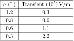
For this apodization function the refractive index and reflection coefficient are illustrated in Fig. 3. It is shown that with increasing the parameter a, which is used in the apodization function, the slope of the transfer function is increased and transient region is decreased. So, using suitable value for this parameter an optimized operation for designed optical switch can be obtained. Table 3 shows some transient region duration for different values of the parameter.
Table 3. Transient duration for different parameters of raised cosine.
a(L) Transient (105) V/m
1.2 0.3
0.8 0.6
0.6 1.1
0.3 2.2
3.3. Quadratic Apodization Function
For third case the quadratic apodization is considered. In this case the index of refraction apodization function is controlled using a parameter named T.
A(z) =
1− T 12 +T
z−0.5L L
2
, (23)
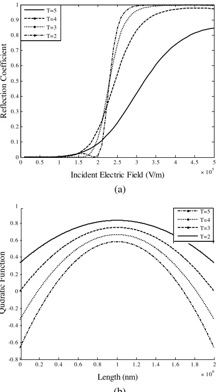
Figure 4 shows variation of the transfer function with changing
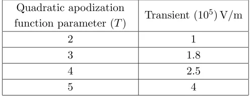
T. Also, in part (b) the apodization function versus the grating length is illustrated. Effect of the parameter (T) appeared in apodization function on switching performance is illustrated. It is observed that with small apodization parameter the switching quality is increased.
0 0. 5 1 1. 5 2 2. 5 3 3. 5 4 4. 5 5 × 10⁵ 0
0. 1 0. 2 0. 3 0. 4 0. 5 0. 6 0. 7 0. 8 0. 9 1
Incident Electric Field (V/m)
R
efle
ctio
n
Co
effic
ie
n
t
T=5 T=4 T=3 T=2
(a)
0 0. 2 0. 4 0. 6 0. 8 1 1. 2 1. 4 1. 6 1. 8 2 × 10⁶ -0. 8
-0. 6 -0. 4 -0. 2 0 0. 2 0. 4 0. 6 0. 8 1
Length (nm)
Q
u
d
rati
c
F
u
n
ct
io
n
T=5 T=4 T=3 T=2
(b)
Figure 4. (a) The reflection coefficient vs. incident electric field and
3.4. Linear Chirp Function
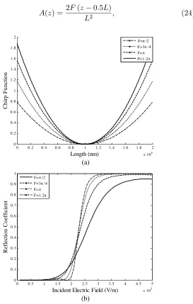
For investigation of the switching performance as a final study, the chirped refractive index is considered. For this purpose the following linear chirp function for modification of the refractive index is adopted.
A(z) = 2F(z−0.5L)
L2 , (24)
0 0. 2 0. 4 0. 6 0. 8 1 1. 2 1. 4 1. 6 1. 8 2 × 10⁶ 0
0. 2 0. 4 0. 6 0. 8 1 1. 2 1. 4 1. 6 1. 8 2
Length (nm)
Chi
rp
F
u
n
ct
io
n
F=π/2 F=3π/4 F=π F= 1.2π
(a)
0 0. 5 1 1. 5 2 2. 5 3 3. 5 4 4. 5 5
× 105 0
0. 1 0. 2 0. 3 0. 4 0. 5 0. 6 0. 7 0. 8 0. 9 1
Incident Electric Field (V/m)
R
eflec
tio
n
Co
efficien
t
F=π/2 F=3π/4 F=π F=1. 2π
(b)
Figure 5. (a) Chirp function vs. grating length and (b) the reflection
whereF is chirp parameter.
The proposed switch with chirp function is studied numerically and the simulated result is illustrated in Fig. 5. Also, numerical data is given in Table 5 too. It is shown that with increasing the chirp parameter the transient duration is decreased. The tunable transfer function using the chirp parameter is illustrated in this figure.
0 0. 5 1 1. 5 2 2. 5 3 3. 5 4 4. 5 5 × 10⁵ 0
0. 1 0. 2 0. 3 0. 4 0. 5 0. 6 0. 7 0. 8 0. 9 1
Re
fl
ec
ti
o
n
Incident Electric Field [V/m]
1+ 0. 1c os (0.25X/X2) 1+ 0. 1c os (0.5X/X2) 1+ 0. 1c os (X/X2)
Figure 6. The reflection coefficient vs. incident electric field.
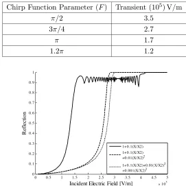
Effects of the other chirp function on switching performance are illustrated in the following figures. In Fig. 6 effect of cosine chirp function on performance of the proposed optical switch is investigated. It is observed that with increasing the spatial frequency of the chirp function the switching threshold is increased.
Table 4. Transient duration for different parameters of quadratic
apodization.
Quadratic apodization
function parameter (T) Transient (10 5) V/m
2 1
3 1.8
4 2.5
Table 5. Transient duration of the transfer function.
Chirp Function Parameter (F) Transient (105) V/m
π/2 3.5
3π/4 2.7
π 1.7
1.2π 1.2
0 0. 5 1 1. 5 2 2. 5 3 3. 5 4 4. 5 5
× 1 05 0
0. 1 0. 2 0. 3 0. 4 0. 5 0. 6 0. 7 0. 8 0. 9 1
R
eflectio
n
Incident Electric Field [V/m]
1+ 0. 1(X/X2) 1+ 0. 1(X/X2) +0.01(X/X2)2 1+ 0. 1(X/X2)+0. 01(X/X2)2
+0.001(X/X2)2
Figure 7. The reflection coefficient vs. incident electric field.
Also, considering effect of the power law chirp function on switching performance, after numerical simulation it is observed that the switching threshold can be controlled.
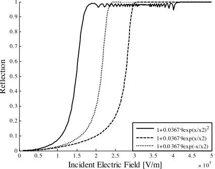
As another example, we consider shifted exponential chirp function and investigate effect of chirping on switching performance. It is shown that in the case of linear power of exponential function small switching threshold is needed.
In the case of nonlinear power of the exponential chirp function small switching threshold is obtained.
0 0. 5 1 1. 5 2 2. 5 3 3. 5 4 4. 5 5 × 10⁵ 0
0. 1 0. 2 0. 3 0. 4 0. 5 0. 6 0. 7 0. 8 0. 9 1
R
efle
ctio
n
Incident Electric Field [V/m]
1+ 0.03679exp((X-X2/2)/X2)2 1+ 0.03679exp((X-X2/2)/X2)
Figure 8. The reflection coefficient vs. incident electric field.
0 0. 5 1 1. 5 2 2. 5 3 3. 5 4 4. 5 5
× 105 0
0. 1 0. 2 0. 3 0. 4 0. 5 0. 6 0. 7 0. 8 0. 9 1
R
efle
ctio
n
Incident Electric Field [V/m]
1+ 0. 0367 9exp(x/x2)2 1+ 0. 0367 9exp(x/x2) 1+ 0.0 367 9exp(-x/x2)
Figure 9. The reflection coefficient vs. incident electric field.
4. CONCLUSION
0 0. 5 1 1. 5 2 2. 5 3 3. 5 4 4. 5 5 × 10⁵ 0
0. 1 0. 2 0. 3 0. 4 0. 5 0. 6 0. 7 0. 8 0. 9 1
R
efle
ctio
n
Incident Electric Field [V/m]
1+ sinc (X/X2) 1+ sinc (2X/X2)
Figure 10. The reflection coefficient vs. incident electric field.
REFERENCES
1. Erdogan, T., “Fiber grating spectra,” J. Lightwave Technology, Vol. 15, No. 8, Aug. 1997.
2. Zhao, J., X. Shen, and Y. Xia, “Beam splitting, combining, and cross coupling through multiple superimposed volume-index gratings,”Optics &Laser Technology, Vol. 33, 23–28, 2001. 3. Hruschka, P. C., U. Barabas, and L. Gohler, “Optical narrowband
filter without resonances,” Ser.: ELEC. ENERG, Vol. 17, 209– 217, 2004.
4. Kulishov, M., “Interdigitated electrode-induced phase grating with an electrically switchable and tunable period,” Applied Optics, Vol. 38, No. 36, 1999.
5. Kulishov, M., “Tunable electro-optic microlense array, I. Planar geometry,” Applied Optics, Vol. 39, No. 14, 2000.
6. Kulishov, M. and X. Daxhelet, “Electro-optically reconfigurable waveguide superimposed gratings,”Optics Express, Vol. 9, No. 10, 2001.
7. Kulishov, M., P. Cheben, X. Daxhelet, and S. Delprat, “Electro-optically induced tilted phase gratings in waveguides,” J. Opt. Soc. Am. B, Vol. 18, No. 4, 2001.
9. Kulishov, M., X. Daxhelet, M. Gaidi, and M. Chaker, “Transmission spectrum reconfiguration in long-period gratings electrically induced in pockels-type media with the help of a periodical electrode structure,”J. Lightwave Technology, Vol. 22, No. 3, 2004.
10. Glytsis, E. N., T. K. Gaylord, and M. G. Moharam, “Electric field, permittivity, and strain distributions induced by interdigitated electrodes on electrooptic waveguides,” J. Lightwave Technology, Vol. 5, No. 5, May 1987.
11. Ramaswami, R. and K. N. Sivarajan, Optical Networks, A
Practical Perspective, Morgan Kaufmann, San Fransisco, CA,
1998.
12. Roberts, G. F., K. A. Williams, R. V. Penty, I. H. White, M. Glick, D. McAuley, D. J. Kang, and M. Blamire, Monolithic 2x2 Amplifying Add/Drop Switch for Optical Local Area Networking, ECOC’03, Vol. 3, 736–737, Sept. 24, 2003.
13. Dugan, A., L. Lightworks, and J. C. Chiao, “The optical switching spectrum: A primer on wavelength switching technologies,” Telecommun. Mag., May 2001.
14. Dobbelaere De, P., K. Falta, L. Fan, S. Gloeckner, and S. Patra, “Digital MEMS for optical switching,”IEEE Commun. Mag., 88– 95, Mar. 2002.
15. Bregni, S., G. Guerra, and A. Pattavina, “State of the art of optical switching technology for all-optical networks,”
Communications World, WSES Press, Rethymo, Greece, 2001.
16. Mukherjee, B.,Optical Communication Networks, Mc-Graw-Hill, New York, 1997.
17. Yariv, A.,Quantum Electronics, John Wiley, 1989.
18. Nishihara, H., M. Haruna, and T. Suhara, Optical Integrated Circuits, McGraw-Hill, 1989.
19. Ghafoori-Fard, H., M. J. Moghimi, and A. Rostami, “Linear and nonlinear superimposed Bragg grating: A novel proposal for all-optical multi-wavelength filtering and switching,” Progress In Electromagnetics Research, PIER 77, 243–266, 2007.