Power factor correction (PFC) of a single phase AC to DC
Interleaved boost Converter by using novel control scheme
Pranali V. Narayane
Department of Electrical Engineering TGPCET, Nagpur, Indai [email protected]
Dr. Hari Kumar Naidu Department of Electrical Engineering
TGPCET, Nagpur, Indai [email protected]
Abstract—In this paper, a controlled two stage single phase ac to
dc three interleaved boost converters power factor correction (PFC) system based on operating with pulsewidth modulation (PWM) technique. Both converters are independently controlled by an inner control loop based on a sliding-mode (SM) approach that imposes minimum current ripple behavior on each cell. The switching of power electronics devices gives an average current control mode so that the power factor (PF) of the converter is high. The SM-based controller is designed to operate at a constant switching frequency so that the L-C filter of interleaving technique, which is recommended for ac–dc power conversion systems is stable and output power is higher than 0.5 kW. An outer loop regulates the output voltage by means of a proportional–integral (PI) compensator directly obtained from a small-signal model of the ideal sliding mode control dynamics. The control law proposed has been validated using numerical simulations and experimental results in a 0.5-kW prototype. IndexTerms—AC–DC power conversion, boost converter, sliding mode control (SMC), interleaving, L-C filter, power factor correction (PFC).
I. INTRODUCTION(HEADING1)
H
IGH power density, high conversion efficiency, high power factor, and low total harmonic distortion (THD) are the desired features expected from onboard plug-in electric vehicle (PEV) battery chargers [1]–[4]. Fig. 1 shows the general power electronic architecture of a typical onboard PEV battery charger. The system consists of a front-end ac/dc converter used for rectification at a unity power factor and a second stage dc/dc converter responsible for battery current regulation and providing galvanic isolation [5],[6]. A comprehensive topological survey of the currently available PEV charging solutions has been presented in [4]. A boost converter is a common front-end PFC interface due to its simple structure, good THD reduction performance, and unity power factor operation capability [7], [8]. However, the volume of the converter tends to increase with the increase in charging power. Moreover, high RMS current in the dc-link capacitors would generate high power loss and significantly reduce the capacitor’s lifetime, leading to capacitor failures. In addition, the required inductance value to reduce the ripples in the input current for better THD performance would considerably increase as the charging power increases [9].This results in a large-volume inductor core and wire size. Compared with a single-phase boost PFC converter, the interleaved boost topology has the benefits of reduced overall volume and improved power density [10]–[12]. In the dc/dc isolation stage, resonant converters are preferable at high-voltage and high-power PEV battery charging applications. In particular, multi-resonance-based LLC topology has several advantages over other resonant topologies, such as 1) good voltage regulation performance at light load condition, 2) the ability to operate with zero-voltage switching (ZVS) over-wide load ranges, 3) no diode reverse recovery losses through soft commutation, 4) low voltage stress on the output diodes and 5) having only a capacitor as the output filter compared with the conventional LC filters [13], [14]. Despite these advantages, operating the circuit at the maximum efficiency considering the conduction and switching losses over the full output voltage ranges remains a challenging issue as the battery voltage varies in a wide range depending on the
different states of charge.
Fig. 1. Block diagram of a two-loop control for a single-phase PFC, AC to DC Rectifier.
II. PROPOSED WORK
controller is most challenging task for DC-DC converters. There are linear and non-linear controllers. Non-linear controllers are more accurate as compared to linear controller [3]. In traditional controller, application of linear control theory based on
linearised
model. A linear control method fails to respond properly to any variation in the operating point and load disturbance. To overcome these issues, nonlinear controller can be used which are more robust and faster dynamic response [4]. There are many non-linear control schemes, such as fuzzy logic control, current-mode control and sliding mode control proposed for DC-DC converter. Due to simple and model free implementation sliding mode control and fuzzy logic control can be applied with satisfactory results [4], [5]. Out of this controller sliding mode control is powerful method which able to makes the system very robust. The system with sliding mode control avoided effects of modeling uncertainties, fluctuations and disturbance of parameter and load variations. The advantages of sliding mode controller are robustness and stability [4]. Due to this reason sliding mode control technique has gained popularity in the applications involving converter and inverters [5].The power sources have quite low–voltage output and require series connection of voltage booster to provide higher output voltage. DC-DC Boost converter is generally used to further boost the voltage to the required level [6]. Other booster converter such as Boost, Buck, Boost series resonant full bridge and push-pull are not recommended due to objectionable ripples in the current flowing out of the renewable energy sources. During electronically extreme thermal excursions it become to develop a high temperature, high power density and high efficiency electrical power system which can be reliably function. To fulfill this requirement interleaved boost converters have been studies in recent years due to their potential to improve power converter performance in terms of efficiency, size, conducted electromagnetic emission and transient response [6], [7]. The power system can have high voltage step up and smaller ripple at the output voltage and output current. As compare with the single boost converter amplitude of input current ripple is less in interleaved boost converter [8], [9]. Interleaved boost converter has low switching loss and faster transient response [10].
II. MODELLINGOFDCTODCBOOSTCONVETER
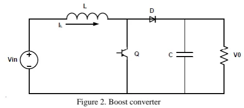
Figure 2. Boost converter .
Fig. 2 shows a DC–DC boost converter. It consists of a DC input voltage source (Vin), a controlled switch (Sw), a diode (D), a filter inductor (L), a filter capacitor (C), and a load resistor (R). The equations describing the operation of the converter can be written for the switching conditions ON and OFF, respectively as
diL/dt = 1/L(Vin) (1)
dv0/dt = 1/C(-V0/R) (2)
And
diL/dt = 1/L(Vin- V0) (3)
dv0/dt = 1/C(1-V0/R) (4)
By Adding equation (1) – (4) Gives
diL/dt = 1/L(Vin- uV0) (5)
dv0/dt = 1/C(u-V0/R) (6)
Where „u‟ is the control input which takes 1 for the ON state of the switch and 0 for the OFF state.
Fig. 3. Model of DC-DC interleaved Boost Converter
Fig. 3 shows model of dc-dc interleaved boost converter. Interleaved boost converter can be simply obtained by operating three boost converters operating 1200 out of phase. The input current is the sum of three inductor currents IL1, IL2 and IL3. As the inductor ripple current is out of phase, they abandon each other and diminish the input ripple current produce by inductor of boost converter.
The output capacitor current is the sum of the three diode currents, I1+ I2+ I3 minus Dc output current, which reduces the dc- output capacitor ripple Iout As a function of duty cycle. The design aspects of Interleaved Boost Converter are given in the below section:
1) Boost Ratio
The boosting ratio of the converter is a function of the duty ratio. It is same as in conventional boost converter. It is defined as
Vdc/ Vin= 1/1-D (7)
2) Input Current
The input current can be calculated by the input power and the input voltage.
Iin = Pin/Vin (8)
Where Pin is the input power, in is the input voltage 3) Inductor current ripple peak -to-peak amplitude
The inductor current ripple peak-to-peak amplitude is given by.
I L1, L2, L3 = Vin*D/fsw*L (9)
Where fsw is the switching frequency, D is the duty cycle, Vin is the input voltage and L is the inductance.
Interleaved boost converter is employed to reduce input and output a voltage ripple which reduces the size of filters since the output current split into N parts it reduces the I2R losses and inductor loss which leads to higher efficiency [6].
B. selection of inductor and capacitor
In recent day magnetic components plays a vital role for energy storage and filtering in power electronic systems. Interleaved boost converter used for transferring the energy from the input voltage to the output voltage. For interleaved boost converter the three inductors are identical for balance the current in the three boost converter.
1) Inductor Selection
The value of inductor can be found by using following formulae [11]
L = Vi Δ (V0-Vi)/ Δ IL Δ fs Δ V0 (10)
Where Vi represents input voltage, V0 represents output voltage, fs represents frequency and Δ IL represents inductor ripple current.
2) Capacitor Selection
The value of inductor can be found by using following formulae [11].
C = Io(max) Δ D/fs Δ Vo (11) Where Δ Vo represents the change in output voltage, fs represents frequency, D represents duty ratio, Io represents maximum output current
V. SIMULATION RESULTS
The boost converter parameters used in simulation are given in table I
TABLE I. SIMULATION MODEL PARAMETERS
Fig. 4. Simulation waveform of input voltage
Fig. 4 shows waveform of single phase ac input voltage which is applied to rectifier.
Fig. 5. Simulation waveform of output voltage
Fig. 5 shows waveform of output voltage of interleaved boost converter.
Fig. 6. Simulation waveform of output current
Fig. 6 shows waveform of output current of interleaved boost converter.
Fig. 7. Simulation waveform of output power
Fig. 8. Simulation waveform of output voltage for change in input voltage
Fig. 8 shows waveform of output voltage which remains unchanged as input voltage change of interleaved dc-dc boost converter.
Fig. 9. Simulation waveform of output voltage for change in input voltage
Fig. 9 shows clearly as change input voltage output voltage does not change for same resistive load.
TABLE II. OUTPUT VOLTAGE AT DIFFERENT INPUT VOLTAGE
As change in the input voltage occurred due to due any uncertainty the output voltage remains unchanged. Output voltage remains stable which is clearly shown by simulation waveform and the values shown in Table. II
TABLE III. OUTPUT VOLTAGE AT DIFFERENT LOAD
As per values shown in table III it is cleared that variations in the load parameters or any uncertainty output voltage remains stable. For same value of input voltage with different load resistance output voltage remains stable which is clearly observed and shown in simulation waveform.
From above explanation it is clear that slide mode control is robust and stable which proves the advantages of slide mode control.
VI. EXPERIMENTAL SETUP
Fig. 14. Experimental setup of a slide mode control dc-dc interleaved boost converter
VII. EXPERIMENTAL RESULTS
The performance of the sliding mode controller is experimentally verified. The specification of the converter is the same as that used in simulation. The experimental results match the simulation very well. Also, it can be seen that the output voltage is a little less than or higher than the desired 650V in each circumstance, due to the parasitic parameters in the hardware circuit, which are neglected in simulation.
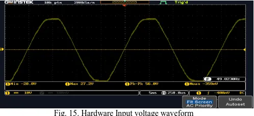
Fig. 15. Hardware Input voltage waveform
Simulation result and the hardware result are differ from each other as it is clearly seen from above result the some harmonics is present in the input of the 50Hz power supply. The result is varying due to the above reasons.
Fig. 16. Pulse generated in hardware
TABLE IV. OUTPUT VOLTAGE AT DIFFERENT INPUT VOLTAGE
From above table output voltage for various input voltage values is given which is more or less than 650v due to the parasitic parameters in the hardware circuit.
Hardware output voltage waveform not possible to show due to the unavailability of higher range DSO, output voltage is measured by using multi-meter and shown in table IV. VIII. CONCLUSIONS
This paper presented a sliding mode controller of dc-dc interleaved boost converter. The various conditions are considered for testing the simulation results. After variation in the input voltage output voltage remains constant. Simultaneously by changing the resistive load in the system of simulation model does not effect on the output voltage. Hardware results also shows the same expected results. Slight variations in the output voltage observed at the time of hardware experimentation. The simulation and hardware result shows that slide mode control is most robust and stable. This method which is proposed in this paper further may be investigated in other topologies of converters.
REFERENCES
[1] Hari Priya T., Alivela M. Parimi, U.M. Rao, ―Development of Hybrid Controller for Photovoltaic Based DC-DC Boost Converter in DC Grid
Connected Applications,‖ International Conference on Circuit, Power and Computing Technologies, 2016.
[2] Carolina Evangelista, Alessandro Pisano, Paul Puleston, Elio Usai, ―Time-based adaptive second order sliding mode controller for wind energy conversion optimization,‖ IEEE Conference on Decision and Control, Loss angeies, California, USA, pp. 2038-2043, December 15-17, 2014.
[3] A. Karthikayini, S. Ramprasath, P. Rameshbabu, ―Modeling and Simulation Of PWM Based Sliding Mode Voltage Controller for Boost Converter In Continuous Conduction Mode,‖ International Conference on Circuit, Power and Computing Technologies, 2015.
[4] Victor Repecho, Domingo Biel, Josep M. Olm, Enric Fossas, ―Switching Frequency Regulation in Sliding Mode Control by a Hysteresis Band Controller,‖ IEEE Trans. On Power Electronics, in press.
[5] Xianggui Guo, Jianliang Wang, Fang Liao, and Rodney Swee Huat Teo, ―Distributed Adaptive Integrated-Sliding-Mode Controller Synthesis for String Stability of Vehicle Platoons,‖ IEEE Trans. On Intelligent Transportation Systems, vol. 17, no. 9, pp. 2419-2429, September 2016. [6] Hammad Sami Khan, Attaullah Y. Memon, ―FIL Simulation of Sliding Mode Controller for DC/Dc Boost Converter,‖ 2016.
[7] Omar Hegazy, Joeri Van Mierlo, Philippe Lataire, ―Analysis, Modeling, and Implementation of a Multidevice Interleaved DC/DC Converter for Fuel Cell Hybrid Electric Vehicles,‖ IEEE Trans. On Power Electronics, vol. 27, no. 11, pp. 4445-4458, November 2012.
[8] Carl Ngai-Man Ho, Hannes Breuninger, Sami Pettersson, Gerardo Escobar, Leonardo Augusto Serpa, Antonio Coccia, ―Practical Design and Implementation Procedure of an Interleaved Boost Converter Using SiC Diodes for PV Applications,‖ IEEE Trans. On Power Electronics, vol. 27, no. 6, pp. 2835-2845, June 2012.
[9] J.S.Anu Rahavi, T.Kanagapriya, Dr.R.Seyezhai, ―Design and Analysis of Interleaved Boost Converter for Renewable Energy Source‖, International Conference on Computing, Electronics and Electrical Technologies [ICCEET], pp. 447-451, 2012.
[10] Antonella Ferrara, Gian Paolo Incremona, ―Design of an Integral Suboptimal Second-Order Sliding Mode Controller for the Robust Motion Control of Robot Manipulators,‖ IEEE Trans. On Control Systems Technology, vol. 23, no. 6, pp. 2316-2325 , November 2015.
[11] M. D. Singh & K. B. Khanchandani, ―Power Electronics‖, Reference Book, pp. 517-518
[12] Siew-Chong Tan, Y. M. Lai, Chi K. Tse, ―A Unified Approach to the Design of PWM-Based Sliding-Mode Voltage Controllers for Basic DC-DC Converters in Continuous Conduction Mode,‖ IEEE Trans. On Circuits and Systems., vol. 53, no. 8, pp. 1816-1827, Augt. 2006.
[13] Siew-Chong Tan, Y. M. Lai, and Chi K. Tse, ―General Design Issues of Sliding-Mode Controllers in DC–DC Converters,‖ IEEE Trans. On Industry Application., vol. 55, NO. 3, pp.1160-1174, March 2008
[14] Mohamed Edardar, Xiaobo Tan, and Hassan K. Khalil, ―Design and Analysis of Sliding Mode Controller Under Approximate Hysteresis Compensation,‖ IEEE Trans. On Control Systems Technology, vol. 23, no. 2, pp. 598-608, , March 2015.
[15] Jin Ye, Pawel Malysz, and Ali Emadi, ―A Fixed-Switching-Frequency Integral Sliding Mode Current Controller for Switched Reluctance Motor Drives,‖ IEEE Journal of Emerging and Selected Topics in Power Electronics, vol. 03, no. 2, pp. 381-394, June 2015.
[18] Jinhui Zhang, Yujuan Lin, and Gang Feng, ―Analysis and Synthesis of Memory-Based Fuzzy Sliding Mode Controllers,‖ IEEE Trans. On Cybernetics, vol. 45, no. 12, pp. 2880-2892, December 2015.
[19] Zengshi Chen, Wenzhong Gao, Jiangang Hu, and Xiao Ye, ―Closed-Loop Analysis and Cascade Control of a Nonminimum Phase Boost Converter,‖ IEEE Trans. On Power Electronics, vol. 26, no. 4, pp. 1237-1252, April 2011. [20] Angel Cid-Pastor, Roberto Giral, Javier Calvente, V. I. Utkin, and Luis Martinez-Salamero, ―Interleaved Converters Based on Sliding-Mode Control in a Ring Configuration,‖ IEEE Trans. On Circuits and Systems-I: Regular Papers, vol. 58, no. 10, pp. 2566-2577, Octomber 2011.
[21] Hendrik Fehr, Albrecht Gensior, ―On Trajectory Planning, Backstepping Controller Design and Sliding Modes in Active Front-Ends,‖ IEEE Trans. On Power Electronics, vol. 31, no. 8, pp. 6044 -6056, August 2016.
[22] Yingying Cheng, Yigang He, ―Comments on Design of Voltage Tracking Control for DC-DC Boost Converter Via Total Sliding-Mode Technique,‖ IEEE Trans. On Industrial Electronics, in press.
[23] Fellipe S. Garcia, José A. Pomilio, Giorgio Spiazzi, ―Modeling and Control Design of the Interleaved Double Dual Boost Converter,‖ in press. [24] Y. He, F.L. Luo, ―Sliding-mode control for dc–dc converters with constant switching frequency,‖ IEE Proc.-Control Theory Appl., vol. 153, no. 1, pp. 37-45, January 2006.
[25] Archana. R. Nikhar, S. M. Apte, Rahul Somalwar, ―Review of Various Control Techniques for Dc-Dc Interleaved Boost Converters‖, International Conference on Global Trends in Signal Processing, Information Computing and Communication, pp. 432-437, 2016.