Walter, Jennifer Jean Huening. Raman Scattering Analysis of Structural Transformations Due to Precision Engineered Si, 6H-SiC and β-Si3N4. (Under the direction of Robert J.
Nemanich)
This thesis explores the local residual structural transformations that result from indentation and ductile material removal of machined Si, 6H-SiC, and β-Si3N4. During
the machining process, very high pressures can be achieved at the contact interface between the machining tool and the surface of a material. The induced pressures can cause transformations through a series of phases, and upon releasing the pressure, the material can again be transformed to a new phase. Many of the high-pressure phases of Si, and some of the phases of SiC and β-Si3N4 have been defined experimentally for
hydrostatic pressure conditions in diamond anvil cell experiments, and have also been predicted theoretically. However, the complexity of plastic deformation complicates the transition process from non-hydrostatic pressure causes the response of the material to be difficult to define for precision engineered and machined surfaces. In these cases, the transmission of applied force can be dependent on nonhydrostatic structural changes due to plastic flow, and structural transitions can be induced at lower pressures than would occur, if at all, for hydrostatic pressures. The Raman technique is employed as a nondestructive structure sensitive probe to investigate the structural and vibrational properties of indented and machined Si, 6H-SiC, β-Si3N4. Visible Raman scattering of Si
materials, 6H-SiC and β-Si3N4, the short absorption depth of UV light allows for accurate
probing of the surface, and the transparency to visible light allows analysis of the bulk material. The studies on indentations made on the 6H-SiC (0001) surface indicate biaxial stress from point pressure. Machined 6H-SiC basal plane edges of (0001) wafers indicate that the near surface structure is changed from single crystal to polycrystalline. Studies conducted on nm and µm precision-machined β-Si3N4 reveals transformation of a surface
Dedication
Biography
Acknowledgements
The author would like to greatly acknowledge the support and guidance of the faculty, students, and staff of the Department of Physics. I would also like to thank the high-pressure phase transformation group, Jae-il Jang, Songqing Wen, George Pharr, John Patten, Lei Dong, Jimmie Miller, Travis Randall, and Ronald Scattergood, for their contributions to the work, fruitful discussions, and for the opportunity to take part in this research project. I would like to thank the SSL group, both past and present, Lena Fitting, Billyde Brown, Dr. Minseo Park, Anderson Sunda-Meya, Dr. Brian Coppa, Dr. Ted Cook, Dr. Jaesob Lee, Mengning Liang, Charlie Fulton, James Burnette, Joe Tedesco, Matt Zeman, Jacob Garguilo, Franz Koeck, Yunyu Wang, Will Mecouch, Dr. Woochul Yang, Eugene Bryan, and Tom Blair, for their help in experiments and analyzing results, in addition to their friendships. I would like to thank our administrative assistants, C.J. Hathorne and Cecilia Upchurch, for always taking care of the SSL group.
I am grateful to my committee members, Ronald Scattergood, Hans Hallen, and Leah Bergman, who have all played a significant role in my education through classes and/or research. I’d like to give special thanks to my advisor, Robert J. Nemanich, for the opportunities and freedom he has given me throughout this research, in addition to, his support, intellectual insight, and guidance.
Table of Contents
List of Figures ...……….……….…... vii
List of Tables…...………..……… xi
Ch. 1: Introduction………... 1
1.1: References……….……….…... 4
Ch. 2: Raman Scattering Analysis of Si, SiC and Si3N4…...………..………... 5
2.1: Origin of the Raman scattering spectrum….………... 5
2.2: Raman scattering modes of Si, 6H-SiC and β-Si3N4.………...……... 6
2.3: Raman scattering analysis of material structures….…...………... 8
2.4: Stress Measurements of Raman scattering modes....………….……...……. 10
2.5: Probing depth dependence on incident wavelength…...……… 12
2.6: References………... 13
Ch. 3: Transformations in Si, SiC and Si3N4……….……… 21
3.1: Transformation Process………... 22
3.2: Transformations in Si………. 23
3.3: Transformations in SiC…..………. 24
3.4: Transformations in Si3N4……..………..…... 24
3.5: References………... 26
Ch. 4: Raman Scattering Analysis of Indented and Machined Si……….……… 29
4.1: Experiment summary………...………... 29
4.2: Experimental details……...………... 30
4.3: Results………...……….………..…... 31
4.5: Conclusions………..………... 36
4.6: References………...………... 37
Ch. 5: UV Raman Scattering Analysis of Indented and Machined 6H-SiC…….………. 46
5.1: Experiment summary………...………... 46
5.2: Experimental details……...………....……... 46
5.3: Results………...……….…...…………. 48
5.4: Discussion………...…………....……...…….… 53
5.5: Conclusions……….………... 55
5.6: References………....…...……... 57
Ch. 6: UV Raman Scattering Analysis of Machined β-Si3N4………....……... 69
6.1: Experiment summary………...…………... 69
6.2: Experimental details……...……… 69
6.3: Results………...……….……...………. 70
6.4: Discussion………...….……...…...……… 72
6.5: Conclusions……….……...……… 81
6.6: References……….…………...……...……... 82
List of Figures
2.1 The phonon dispersion curve for 6H-SiC in the large zone………...14 2.2 Micro Raman scattering of Si chips showing the crystalline Si peak at 520Rcm-1
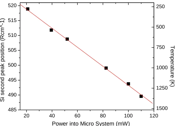
and a heated peak at lower relative wavenumbers. The spectra (a) to (d) are from lower to higher power, respectively………...17 2.3 The peak position of the Raman scattering spectra from Si chips versus laser
power. The vertical scale on the right represents the temperature that would correspond to the observed Raman scattering peak shift………...…18 2.4 Decay of the Raman scattering signal with depth in the sample for (a) single
crystal Si (b) single crystal 6H-SiC and (c) β-Si3N4. The probing depth is defined
as the depth where the intensity is 37% of the incident……….……19 3.1 Micro Raman scattering spectra of three SiC wafers which show the dominant TO modes at ~760Rcm-1 and the LO modes at ~ 970Rcm-1 for (a) 4H-SiC, (b) 6H-SiC, and (c) a mixture of 4H and 6H SiC………..28 4.1 One-step load displacement curves for (a) 100 and (b) 200 mN maximum load
indents. An indentation rate of 5 mN/s was employed……….…38 4.2 SEM images of Si indentations for maximum loads of (a) 100, (b) 200, and (c)
700 mN. An indentation rate of 5 mN/s was employed………39 4.3 Micro Raman scattering spectra taken from the center of a Si indentation obtained with a maximum load (a) 100, (b) 200, and (c) 700 mN………...40 4.4 Schematic of the typical damage pattern observed from machined (001) and (111)
4.5 Macro Raman scattering spectra of machined Si (111) wafer machined in the
[110] direction with a rake angle of -45° and with a feed rate of (a) 5 and (b) 1 µm/rev………42
4.6 Macro Raman scattering spectra of machined Si (001) surfaces for rates varying from (a) 15 (b) 7 (c) 3 (d) 2 to (e) 1 µm/rev. The surfaces were machined in the
[010] direction………43 4.7 Macro Raman scattering spectra of machined Si (111) surfaces with a rake angle of (a) –25° and (b) -45°. The machining rate was 1 µm/rev., and the direction of
cut was along [110]………44 4.8 Macro Raman scattering spectra of a machined Si (111) wafer with a rake angle
of -45° and feed rate 1 µm/rev. for ductile machining wafer directions of (a)
[110], (b) [112], and (c) [112]……….45 5.1 Schematic (a) of the machining process and (b) 6 fold symmetry directions of 6H-SiC (0001) wafer………58 5.2 The load displacement curve for indentation of a 6H-SiC(0001) surface with a
maximum load of 200 mN……….59 5.3 An SEM image of the surface of indented 6H-SiC. A maximum load of 200 mN
was used……….60 5.4 UV micro Raman scattering spectra display the TO and LO modes for (a) center
of the indent (b) edge of the indent (c) surrounding area (d) reference area for indentation with a maximum load of 200 mN………...61 5.5 The local stress (in units of pressure) in regions in and surrounding an indent.
scattering modes. The results were obtained from indents produced from a maximum indentation load of 200mN, and the stress was deduced using the relations from Liu, et al.……….62 5.6 Polar plot of the cutting force dependence on the 6-fold symmetry of 6H-SiC
machined wafer edges. The plot was obtained for a rake angle of 0°, and a cutting depth of 100 nm……….…63 5.7 Optical image of ductile chip removal. A rake angle of -45°, and a depth of cut of
500 nm were employed………..64 5.8 UV macro Raman scattering spectrum of (a) machined 6H-SiC edge and (b)
polished wafer. For comparison, the (c) calculated vibrational density of states (DOS) of SiC is presented………..65 5.9 UV micro Raman scattering spectra of machined 6H-SiC edges for rake angles of (a) -45°, (b) -30°, and (c) 0°. The spectra were obtained with incident light along the [11 2 0] direction of the wafer………..66 5.10 UV macro Raman scattering spectra of machined 6H-SiC edges for machining
depths of (a) 50, (b) 250, and (c) 500 nm depth of cut per revolution. The spectra were obtained with the incident light along the [11 2 0] direction of the wafer………..67 5.11 UV micro Raman scattering spectra of a (a) dark spot on the machined surface (b)
List of Tables
2.1 The vibrational frequencies are given for (a) propagation angles relative to the c -axis and (b) the weaker modes are valid for any propagation direction and are assigned to values of in the large zone. All values are experimental except the figures in parenthesis, which are calculated……….…15
max
/q q x=
2.2 Backscattering first-order Raman scattering active modes of β-Si3N4 in
Rcm-1……….……….……16
1. Introduction
As technology advances lead to the development of higher precision products, a demand to understand the structural properties of precision engineered materials on a µm and nm
scale is required. The knowledge could be used to enhance macroscopic properties through, for example, patterning of nano scale phases with unique electrical, mechanical, or optical characteristics or optimization of micromachined wafer surfaces by establishing machining parameters that will increase ductility. A scientific basis for these practices can be established from investigation and characterization of structural changes in the materials. The processes in which one structure transforms to another have yet to be fully understood. For instance, there are over 200 polytypes identified in SiC,1 but little work has been done to understand the transformations between them. This thesis is devoted to the identification of structural changes on the surfaces of precision engineered and machined single crystal Si, single crystal 6H-SiC, and polycrystalline β-Si3N4.
The materials chosen for study are brittle, but they have the potential to undergo transformation with the application of high pressures. Si has been widely studied and structural transformations resulting from the application of high-pressures have been characterized by several researchers.2 Of particular interest is the ductility of this material, which is thought to derive from a complex series of transformations during the machining process. Diamond anvil cell experiments have confirmed that under high nearly hydrostatic pressures (~13 GPa) Si will be transformed to a metallic β-Sn phase3
and has been reported to relax to either a metastable Si III phase3 or an amorphous phase depending on the rate in which the pressure was applied. The same residual metastable and amorphous phases have been detected on the surfaces of precision-engineered materials providing evidence that the β-Sn phase is attainable from localized pressures,
which consequently result in plastic flow. Additional diamond anvil cell experiments have reported a decrease in the onset of the transition pressure to the metallic phase from ~11.3 GPa for hydrostatic stresses to ~8.5 GPa for uniaxial stress.4 These measurements indicate that the nonhydrostatic component of stress plays a role in the transformation process. The observed ductility of the material may be directly related to the extent of the residual phases after machining. The phenomenon observed in the investigations on Si is now being expanded to the ceramic semiconductors, 6H-SiC and β-Si3N4.
can be sampled. Visible Raman spectroscopy can be applied to Si, however, for the wide bandgap materials of 6H-SiC and β-Si3N4, visible light penetrates throughout the
material, and UV light must be used to analyze the surfaces. The surface layer thickness affected by the external mechanical forces range from nm to µm. A probing depth less than 35 nm for SiC and less than 1.4 µm for Si3N4 can be achieved with UV excitation.
1.1 References
1. A. Addamiano, in Silicon Carbide-1973, edited by R.C. Marshall, J. W. Faust, Jr. and C.E. Ryan, University of South Carolina, Columbia 179, (1974).
2. Raman Scattering Analysis of Si, SiC and Si3N4
2.1 Origin of the Raman scattering spectrum
The vibrational spectrum of a solid can be described by a frequency distribution (i.e. density of states) or a set phonon dispersion curves, which relate the frequencies and wavevectors of each of the allowed modes. Momentum conservation requires that only phonons that have a projection onto the incident and scattered light fields will scatter light. Therefore, since light exhibits a wavevector k ≈11000 of the Brillouin zone
boundary wavevector, Raman scattering measures k≈0 phonons. The phonons at the zone center are dependent on the number of atoms in the unit cell. They are comprised of acoustic phonons, in which the atoms in each unit cell vibrate in phase with one another, and optic phonons, in which the atoms in the unit vibrate with respect to one another. There are 3 acoustic vibrations and 3(n−1) optic vibrations, where is the number of atoms in the unit cell. The frequencies of vibration depend on the bonding of the atoms within the unit cell.
n
The scattering efficiency depends on the polarization of the incident and scattered lights and is given by
2
∑
⋅ ⋅ = j s j i R e eC
I (2.1)
Here, Cis a constant,Ris the Raman tensor of phonon , and and are the
polarization vectors of the incident and scattered light, respectively. For a complete review of the scattering efficiency in crystals, Loudon has derived the Raman tensors for
the 32-crystal classes.1 All Raman measurements presented in this thesis are the Stokes shifted spectra. The notation, Rcm-1, represents the wavenumber shift of the observed mode from the incident laser frequency.
2.2: Raman scattering modes of Si, 6H-SiC and β-Si3N4
A. Raman scattering modes of Silicon
The structure of Si in its stable form is diamond cubic and is of the space group
. The first order Raman spectrum of crystalline Si at room temperature has a triply degenerate peak at 520 relative wavenumbers with a full-width at half maximum (FWHM) of 3.122cm
m Fd3
h O7
-1
. The Raman spectrum of amorphous Si has two main bands at 150 Rcm-1 and 480 Rcm-1, which are commonly assigned as transverse acoustic (TA) and transverse optic (TO) bands.2 It has been found that the TA/TO intensity ratio and the TO linewidth increases with increasing degree of structural disorder.3
B. Raman scattering modes of 6H-Silicon Carbide
The crystal structure of 6H-SiC is uniaxial with a hexagonal structure and 6-fold
symmetry. 6H-SiC is of the space group . The zone center normal modes are given
by the irreducible representation
4 6v C
) (
6 A1+B1+E1+E2 =
Γ where the , , and
modes are Raman active, and the and modes are also infrared active. There are 12 atoms per unit cell, and therefore, 33 optic phonons and 3 acoustic phonons. The modes in which the Si and C sublattices vibrate against each other include the transverse optic TO modes (vibrations perpendicular to the c-axis) with and
1
5A 5E1 6E2
1
A E1
1
symmetry.4 In the 180° backscattering geometry, the symmetry becomes and for
the TO modes and for the LO mode. Additional weaker modes are observed for 6H-SiC. The symmetries of these modes and the modes of the various polytypes of SiC have been previously assigned.
1
E A1
1
E
5,6
The phonon dispersion curve for 6H-SiC is provided in Fig. 1 and is represented in the large zone scheme extending to 6π a where is the lattice
constant of a unit cell. Since
a
a
π
2 is a reciprocal lattice vector, the pseudomomentum vectors q=0, q=2π a, q=4π a, q=6π a are all equivalent to the point in the
Brillouin zone. The corresponding frequencies and symmetries are listed in Table 1, where it is assumed that the incident laser propagates parallel to the -axis. The broadened phonon density of states of amorphous SiC has broadband features in the range of 650 Rcm
0
= q
c
-1
to 1700 Rcm-1.7
C. Raman scattering modes of β- Silicon Nitride
The β-Si3N4 crystals are hexagonal in structure and belong to the space group
. The irreducible representation for the β-Si
) / 6
( 3
2
6 P m
C h 3N4 zone center phonons is given
by Γoptic =4Ag +2Au +3Bg +4Bu +2E1 +5E2g +4E1u +2E2u, and Γacoustic =Au +E1u. The
2.3: Raman scattering analysis of material structures
The Raman scattering matrix element will affect the relative intensity of the sharp modes from crystalline materials and the broad bands of amorphous materials. In addition to stress effects, careful attention must be given to discerning between polycrystalline, nanocrystalline, amorphous, and highly dislocated material. Moreover, a distinction between the Raman spectrum of the various structures and heated material should be made when using high power densities in micro Raman experiments.
The Raman spectrum for finite crystal domains has been previously explained with a phonon confinement model.9, 10 The wavevector of the vibrational excitation is uncertain by a factor of ∆k=2π /L, where is the crystal dimension, and therefore, the wavevector selection rules for Raman scattering from a finite sized crystal will be uncertain to this degree. Considering that the Brillouin zone boundary is
L
a
/
π , where
is the lattice constant, this effect becomes significant in the Raman spectrum when crystal domains are less than 100 nm. Based on this model and experimental observations, relaxation of the k-vector selection rules will cause the full width at half maximum (FWHM) of the Raman peaks to increase with decreased grain size. A shift in frequency can also occur. In the limit where the domain size decreases to zero and the structure resembles a random network, the material is amorphous, all of the Raman modes become active, and the spectrum resembles the density of states.
a
scattered light. Therefore, the spectra will often resemble the broadened density of states. The relative intensity of specific bands is also enhanced or suppressed depending on the Raman matrix element.
A Raman spectrum of a crystal is dependent on the long-range order, and therefore, a small number of dislocations may not be detected. However, highly dislocated material will decrease the Raman phonon lifetime leading to peak broadening. For very high dislocation densities the phonon scattering length will be significantly resemble amorphous material.
Raman frequency and is given in Fig. 3 for the observed peak shifts and measured power into the microscope. A linear fit is made to the data points and can be extrapolated to the 520 Rcm-1 at 300 K.
2.4 Stress Measurement of Raman scattering modes
A frequency displacement of a peak in a Raman spectrum can often be directly related to the stress of the material. In general, a displacement of a crystalline peak to a lower relative wavenumber in the Stokes Raman spectrum indicates tension, and a displacement to a higher relative wavenumber indicates compression. If the stress is directional and the symmetry of the crystal is broken, the degeneracy of a degenerate vibration can be lifted.
The line shape and line width may convey information about the physical identity of the stresses. The theory of spectral line shape predicts that the line width is inversely proportional to the phonon lifetime and that the line shape can be described by a Lorentzian function: 2 0 0 )) 5 (. ) (( 1 ) ( ω ν ν υ − + = I
I (2.2)
Here I0 is the maximum intensity, ν0 is the central Raman frequency and ω is the line
Inhomogeneous line broadening is due to a distribution of the central Raman frequency within the collection volume of material. In this case, the peak can in theory be fitted as a distribution of Lorentzian peaks and the line then takes on a Gaussian shape:
2
0 ) )
( 6651 . 1 ( 0 )
(ν =I e − ν −ν ω
I (2.3)
where I0 is the maximum intensity, ν0 is the central Raman frequency and ω is the line
width.
In experimental analysis, for the highest accuracy, the Raman peaks are fitted to a Lorentzian function or a mix of Lorentzian and Gaussian functions to determine the center frequency and full width at half maximum. Stress measurement is usually deduced from the center position of the fitted Raman peak. However, a broadened peak could result from a distribution of stresses within the collection volume of material. In this case, the peak can in theory be fitted as a distribution of Lorentzian peaks enveloped within a Gaussain function. A broadened peak could also result from the lifting of the degeneracy in a mode (i.e. the splitting of a degenerate mode).
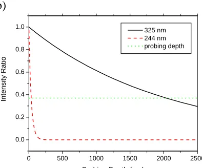
2.5 Probing depth dependence on incident wavelength
The collection volume in the Raman scattering experiment is determined by the probing depth and the focusing resolution, which are dependent on the excitation wavelength. The intensity of light decays in a material following the relationship:
z oe I
I = −α (2.4)
where I0is the incident intensity, α is the absorption constant, and is the distance from
the surface. Conventionally, the probing depth is defined at the point where and
can therefore be calculated as
z
o I I =.37
, 2
1 α
=
y since the light travels both in and out of the material. The absorption coefficient, α, is dependent on the energy of the incident light and the imaginary component of the index of refraction of the material. In this simple analysis, it is assumed that α is the same for both the incident and Raman scattered light.
2.6 References
1. R. Loudon, Adv. Phys. 13, 423 (1964).
2. J.E. Smith, Jr. M.H. Brodsky, B.L Crowder, and M.I. Nathan, Phys. Rev. Lett. 26, 642 (1971).
3. J.S. Lannin, L.J. Pilione, S.T. Kshirsagar, R. Messier, and R.C. Ross, Phys. Rev. B 26, 3506 (1982).
4. D.W. Feldman, J.H. Parker, Jr., W.J. Choyke, and L. Patrick, Phys. Rev. 170, 170 (1968).
5. D.W. Feldman, J.H. Parker, Jr., W.J. Choyke, and L. Patrick, Phys. Rev. 173, 787 (1968).
6. Priscilla J. Colwell and Miles V. Klein, Phys. Rev. B 6, 498 (1972).
7. A. Chehaidar, R. Carles, A. Zwick, C. Meunier, B. Cros, J. Durand, Jour. Non-Crys. Sol. 169, 37 (1994).
8. N. Wafa, S.A. Solin, J. Wong, and S. Prochazka, J. Non-Crys. Solids 43, 7 (1981). 9. R.J. Nemanich, S.A. Solin, R.M> Martin, Phys. Rev. B 23, 6348 (1981).
10. H. Richter, Z.P. Wang, L. Ley, Solid State Commun. 39, 625 (1981).
11. D.W. Feldman, J.H. Parker, Jr., W.J. Choyke, and L. Patrick, Phys. Rev. 170, 170 (1968).
12. K. Honda, S. Yokoyama, S. Tanaka, J. Appl. Phys. 85, 7380
(a)
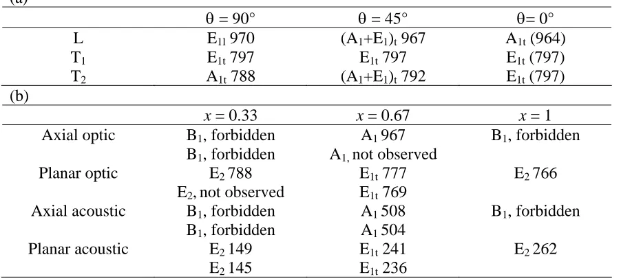
θ = 90° θ = 45° θ= 0°
L E1l 970 (A1+E1)t 967 A1t (964)
T1 E1t 797 E1t 797 E1t (797)
T2 A1t 788 (A1+E1)t 792 E1t (797)
(b)
x = 0.33 x = 0.67 x = 1
Axial optic B1, forbidden A1 967 B1, forbidden B1, forbidden A1, not observed
Planar optic E2 788 E1t 777 E2 766
E2,not observed E1t 769
Axial acoustic B1, forbidden A1 508 B1, forbidden
B1, forbidden A1 504
Planar acoustic E2 149 E1t 241 E2 262
E2 145 E1t 236
TABLE 1: The vibrational frequencies are given for (a) propagation angles relative to the c-axis and (b) the weaker modes are valid for any propagation direction and are assigned to values of in the large zone. All values are experimental except the figures in parenthesis, which are calculated.
max
/q q x=
460 480 500 520 540
Int
ens
ity
(
a.u.
)
Raman shift (Rcm-1)
a b c d
20 40 60 80 100 120 485 490 495 500 505 510 515 520 Si secon d pe ak p ositio n (Rcm^ -1 )
Power into Micro System (mW)
1500 1250 1000 750 500 250 T e mpera ture (K)
(a) (b)
0 200 400 600 800 1000
0.0 0.2 0.4 0.6 0.8 1.0 In ten s it y R a ti o
Probing Depth (nm)
514.5 nm 457.9 nm probing depth
0 500 1000 1500 2000 2500
0.0 0.2 0.4 0.6 0.8 1.0 In tens it y R a ti o
Probing Depth (nm)
325 nm 244 nm probing depth
(c)
0 2000 4000 6000 8000 10000 12000 14000
0.0 0.2 0.4 0.6 0.8 1.0 In ten s it y R a ti o
Probing Depth (nm)
257 nm 244 nm probing depth
Probing Wavelength (nm)
Probing depth Si (nm)
Probing depth 6H-SiC (nm)
Probing depth β -Si3N4 (nm)
244 -- 34.72 1366
257 -- 80.39 4273
325 -- 2050 --
488 247.2 transparent transparent
514.5 331.6 transparent transparent
3. Transformations in Si, SiC and Si3N4
3.1 Transformation Process
machined surfaces provides evidence that the material may have relaxed from a metallic or another denser phase.
Extensive investigations of Si have indicated transformations to different residual phases for diamond anvil cell pressures and point pressures where the residual metastable phases are dependent on the rate of decompression.1 Conversely, investigation of the high-pressure phases and phase transformations of SiC and Si3N4 have been limited.
3.2 Transformations in Si
Wide ranges of study from experiments and calculation have determined the structures of Si under high pressures. Under nearly hydrostatic conditions, Si-I transforms to Si-II (β -tin) in the pressure range of 9 to 16 GPa.2, 3, 4, 5 The metallic β-Sn phase transforms to a phase with Imma symmetry at ~13.2 GPa, and the Imma phase transforms to a simple hexagonal (sh) phase at ~15.4 GPa.6 At ~38 GPa the sh phase transforms to a base-centered orthorhombic structure with Cmca symmetry, and at ~42 GPa the Cmca phase transforms to a hexagonal closed packed (hcp) structure.7 At about ~80 GPa the hcp transforms to a face centered cubic (fcc) phase.8
formed, and on further pressure release, the degree of rhombohedral distortion diminishes gradually, producing a mixture of Si-XII and Si-III (bc8body-centered cubic).12, 13 The Si-XII is found to persist to ambient pressure. For fast decompression, an amorphous Si phase can result.14, 15 Annealing will result in the transformation back to the Si-I parent phase.
3.3 Transformations in SiC
The lattice planes of SiC are composed of Si-C double layers that are parallel to the (0001) plane, and the packing axis is along the [0001] face. SiC is predicted to compress to a metallic16, 17, 18 or rocksalt19, 20, 21, 22 phase, but the mechanism of transformation is not well understood. Experiments have indicated a phase transition in 3C-SiC (zb structure) to a rocksalt (NaCl) phase at ~100 GPa.23 Theoretical first principle LDA calculations indicate that the NaCl form becomes favorable at pressures of ~66 GPa.24 In addition, a phase transition of 6H-SiC to an undetermined phase has been reported subject for shock compression.25 Analyses of the specific phases that result from pressure release are limited for this material.
Polytypism originates from differences in the stacking sequences of the silicon-carbon pair hexagonal layers and may be arrayed in the cubic, hexagonal, or rhombohedral crystal structures. Numerous studies have been reported on transformations between polytypes as a function of temperature and/or pressure by both solid-state mechanisms and diffusion processes.26, 27 For example, a TEM study of indentations performed at
polycrystalline material, and it was observed that some of the grains undergo transformation from the 6H-SiC structure to the 3C-SiC structure through the formation of Shockley partial dislocations lying on the cross-slip plane.28 In a six-layer period of the 6H-polytype, which consists of two three layered microtwins, one of the microtwins can be untwinned by the passage of three partial dislocations with the same ½ <1010> Burgers vector, thus converting the 6H period into two identical 3C periods. The dislocation model for the transformation requires a pinned segment of a screw dislocation that dissociates into two 30 degree partials on the basal plane, a temperature range where there is a large difference in the mobility of the two 30 degree partial dislocations, a sufficiently high resolved shear stress on the primary glide plane to form a faulted loop from the highly mobile leading partial, and a sufficiently large resolved shear stress on the cross-slip plane to make the screw dislocation cross-slip after it has been formed.
To demonstrate the differences in Raman spectra for the various polytypes, Fig. 1 shows the Raman spectra of 4H-SiC, 6H–SiC, and a sample that contained a mixture of 4H-SiC and an unknown polytype.
3.4 Transformations in β-Si3N4
Investigations of the high-pressure phases of β-Si3N4 are very limited. However, preliminary diamond anvil cell experiments conducted by a member of our group (Patten) has revealed low energy x-ray diffraction peaks at pressures between 20 GPa and 35 GPa, which are a signature of the high pressure phase of silicon nitride.29 The diffraction peaks were shifted to smaller angles indicating that the transformed material was denser than the starting phase.
References
1. V. Domnich, Y. Gogotsi, Experimental Methods in the Physical Sciences 38, 355 (2001).
2. H. Olijnyk, S.K. Sikka, and W.B. Holzaffel, Phys. Lett. A 103, 137 (1984). 3. S. Minomura and H.G. Drickamer, J. Phys. Chem. Solids 23, 451 (1962). 4. J.C. Jamieson, Science 139, 762 (1963).
5. J.Z. Hu, L.D. Merkle, C.S. Menoni, I.L. Spain, Phys. Rev. B 34, 4679 (1986). 6. S.P. Lewis, M. L. Cohen, Phys. Rev. B 48, 16144 (1993).
7. N. E. Christensen, D.L. Novikov, M. Methfessel, Solid State Commun 110, 615 (1999). 8. R. J. Needs, A. Mujica, Phys. Rev. B 51, 9652 (1995).
9. B. G. Pfrommer, M. C toˆ e′, S.G. Louie, M.L. Cohen, Phys. Rev. B56, 6662 (1997a). 10. J. Crain, G.J. Ackland, J.R. Maclean, R.O. Piltz, P.D. Hatton, and J. Crain, Phys. Rev. B 50, 13043 (1994).
11. R.O. Piltz, J.R. Maclean, S.J. Clark, G.J. Ackland, P.D. Hatton, and J. Crain, Phys. Rev. B 52, 4072 (1995).
12. R.H. Wentorf and J.S. Kasper, Science 139, 338 (1963). 13. J. S. Kasper and S.H. Richards, Acta Crystall. 17, 752 (1964).
14. D.R. Clarke, M.C. Kroll, P.D. Kirchner, R.F. Cook, B.J. Hockey, Phys. Rev. Lett. 60, 2156 (1988).
15. D.L. Callahan and J.C. Morris, J. Mater. Res. 7, 2907 (1992). 16. J. A. Van Vechten, Phys. Rev. B 7, 1479 (1973).
19. N.E. Christensen, S. Satopathy, and Z. Pawlowska, Phys. Rev. B 35, 1032 (1987). 20. K. J. Chang and M. L. Cohen, Phys. Rev. B 35, 8196 (1987).
21. B.H. Cheong, K.J. Chang, and M.L. Cohen, Phys. Rev. B 44, 1053 (1991). 22. A. Garcia and M. L. Cohen, Phys. Rev. B 47, 4215 (1993).
23. M.A. Yoshida, M. Onodera, M. Ueno, K. Takemura, and O. Shimomura, Phys. Rev. B 48, 10587 (1993).
24. K. J. Chang and M.L. Cohen, Phys. Rev. B 35, 8196 (1987). 25. T. Sekine, T. Kobayashi, Phys. Rev. B 55, 8034 (1997).
26. P. Krishna, R.C. Marchall, and C.E. Ryan, J. Crystal Growth 8, 129 (1971).
27. G.A. Bootsma, W.F. Knippenberg, and G. Verspui, J. Crystal Growth 8, 341 (1971). 28. J. W. Yang and P. Pirouz, J. Mater. Res. 8, 2902 (1993).
700 750 800 850 900 950 1000
In
ten
s
it
y
(a.u.
)
Raman shift (Rcm-1)
a b c
4. Raman Scattering Analysis of Indented and Machined Si
Jennifer J.H. Walter,1 Travis Randall,1 Jae-il Jang,2,3 George M. Pharr,2, 3 Ronald O. Scattergood,1 Robert J. Nemanich1
1North Carolina State University, Raleigh, NC 27695 2University of Tennessee, Knoxville, TN 37996
3Oak Ridge National Laboratory, Oak Ridge, TN 37830
4.1. Experiment Summary
4.2 Experiment Details
The indentation experiments were performed on a single crystal Si (001) wafer. The machining experiments were performed on single crystal Si (111) and Si (001) wafers.
The indentations were made using a Nanoindenter-XP (MTS, Oak Ridge, TN). A Berkovich diamond indenter tip shaped as a three-sided pyramid with a centerline-to-face angle, Ψ, of 65° was used to create triangular shaped indentations. The tip was brought
into contact with the material with loads of 100, 200, and 700 mN, and at a constant loading rate 5 mN/sec.
A Rank Pneumo ASG 2500 Diamond Turning Machine was used to turn various orientations of the silicon wafers at room temperature as a function of feed rate from 1 to 15 µm/rev. The rate is defined as the distance traveled inward or outward across the wafer surface per revolution. Tool rake angles of -30o and -45o were employed with a 3mm radius rounded tool. Machining runs on Si were subject to tip wear and damage considerations as evidenced by the repeated patterns of tip damage features displayed into the machined part surface. However, tool wear was not considered to be an issue since surfaces turned within the ductile regime had RMS values in the range of 1 to 10 nm. The lower RMS roughness values corresponded to the low feed rates, and the higher RMS roughness values corresponded to high feed rates.
spot size of ~ 100 µm x ~2 mm was focused on the sample. In the micro system, a 180° backscattering geometry was employed and a spot size of ~2 µm was incident on the sample. The Raman experiments were performed with the 514.5 nm line of an argon ion laser (Coherent Inc.), and the scattered light was focused onto the entrance slit of a double grating scanning monochromator (ISA U-1000). For measurements on the Si (001) surfaces, careful attention was given to keeping the crystal orientation relative to the polarization of the incident laser light consistent, which will allow comparison of amorphous and crystalline peaks.
4.3 Results A. Indents
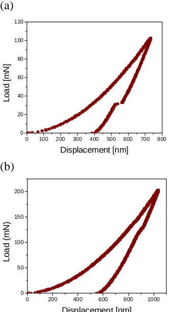
Indentation experiments were performed on a Si (001) surface to investigate local bonding arrangements from controlled point pressure conditions. The load displacement curves for maximum indentation loads of 100 and 200 mN, and an indentation rate of 5 mN/s are provided in Fig. 1. A pop-out feature in the unloading portion of the curve is detected for the 100 mN load. A smaller pop-out feature is also observed for the 200 mN in the load displacement curve. These features have previously been explained by a phase transition accompanied by a volume change in the Si structure.3
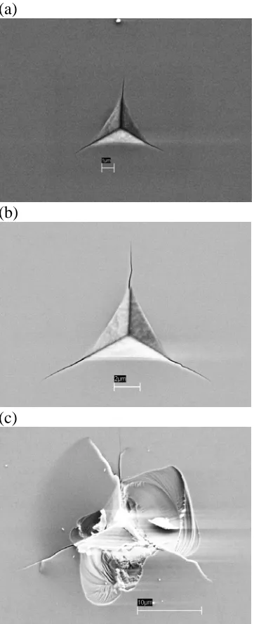
highly cracked while the indented region of the 200 mN load indicate limited cracking. The indented regions of the 100 mN indent indicates no evident macro cracking.
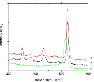
The Raman scattering spectra of the 200 and 700 mN indentations are provided in Fig. 3. The 200 mN indent indicate additional peaks with the center positions located at 352, 375.5, 384, and 434 Rcm-1. The Raman peaks positions have been previously assigned to Si III and Si VII.4 There is also a small, broadened peak indicated at 480 Rcm-1. This peak is commonly assigned to amorphous Si. The 520 Rcm-1 crystalline peak is displaced to higher relative wavenumbers to a center frequency of 522 Rcm-1. This peak displacement indicates residual compressive stress in the indent. The 700 mN load indent indicates a crystalline peak with center frequency at 520 Rcm-1 and a second peak shifted to lower relative wavenumbers at 513 Rcm-1. At lower powers it is shifted toward the crystalline Si peak at 520 Rcm-1. Thus indicating that this second peak at lower wavenumbers is due to laser heating of the cracked regions and the chips surrounding the indent.
B. Machined Surfaces
mild damage, and the white areas represent ductile regions. The damage patterns observed on the Si machined surfaces are in agreement with the predicted fracture pattern with this model. On our machined surfaces, the surface areas of the ductile regions were found to increase with slower feed rates and for larger negative rake angles.
Fig. 5 presents macro Raman scattering spectra obtained from a machined Si (111) wafer for feed rates of 5 and 1 µm/rev. A rake angle of -45° was employed, and the spectra
were obtained from the [110] wafer direction. This direction corresponds to a ductile region of the wafer. A significant decrease in the crystalline Si peak, and an increase in the amorphous peak are observed.
Macro Raman scattering measurements of a machined Si (111) surface for rake angles of -45° and -25° are provided in Fig. 7. The machining rate was 1 µm/rev., and for the
[110] wafer direction. This direction corresponds to a ductile region of the wafer. Both rake angles show the presence of a 480 Rcm-1 feature indicating an amorphous layer and the 520Rcm-1 crystalline Si peak, however, the peak intensity ratios of amorphous to crystalline Si is found to be greater for the larger negative rake angle. This indicates that the amorphous surface layer is greater for a larger negative rake angle.
Fig. 8 shows macro Raman scattering spectra of machined Si (111) surfaces obtained with a rake angle of -45° and a feed rate of 1 µm/rev. The spectra were obtained along the
[110], [112], and [112] wafer directions. The wafer directions correspond to ductile regions of the wafer. The Raman scattering spectra indicate no significant difference in the extent of the amorphous layer for these difference directions.
4.4 Discussion
accommodate the necessary displacements.6 Therefore, a maximum load threshold exists where fracture and cracking become dominant over a phase transition.
On the machined Si surfaces, a ductile and brittle response is found to have orientation dependence on the wafer surface relative to the machining tool. Machining with lower machining rates increased the surface areas of ductile material. Raman scattering of the ductile-machined surfaces does not indicate significant differences in the amorphous layer thickness for the ductile-machined crystal orientations. However, the Raman scattering measurements of the ductile turned surfaces indicated an amorphous layer that was thinner for higher feed rates, and also for smaller negative rake angles. The extent of the amorphous layer is greater when machining at a lower rate. A plausible explanation for a thinning layer with increased feed rate is that more material is machined away as debris. The extent of the amorphous layer is found to be greater for larger negative rake angles. This could be due to higher pressures generated at the contact interface between the machining tool and the material for larger negative rake angles. In addition, with increased feed rates and smaller negative rake angles, it was found that the fractured surface regions increase, while the surface area of ductile response decreases. This effect can be explained with the stress orientation model for diamond cubic surfaces. 7
metallic phase could explain the ductile response observed from point pressure on this brittle material.
4.5. Conclusions
4.6References
1. D. R. Clarke, M.C. Kroll, P.D. Kirchner, R.F. Cook, Phys. Rev Lett. 60, 2156 (1998). 2. H. Olijnyk, S.K. Sikka, and W.B. Holzaffel, Phys. Lett. A 103, 137 (1984).
3.V. Domnich, Y. Gogotsi, S. Dub, Appl. Phys. Lett. 76, 16 2214 (2000).
4.V. Domnich, Y. Gogotsi, Experimental Methods in the Physical Sciences 38, 355 (2001).
5. W.S. Blackley and R.O. Scattergood, J. Am. Ceram. Soc. 73, 10 3113 (1990).
6. S.V. Hainsworth, A.J. Whitehead, and T. F. Page, in “Plastic Deformation of Ceramic” (R.C. Bradt, C.A. Brooks, and J.L. Routburt, Eds.) 173, Plenum Press, NY (1995).
(a)
0 100 200 300 400 500 600 700 800 0 20 40 60 80 100 120 Loa d [ m N ] Displacement [nm] (b)
0 200 400 600 800 1000 0 50 100 150 200 Lo a d ( m N ) Displacement [nm]
(a)
(b)
(c)
FIG 3: Micro Raman scattering spectra taken from the center of a Si indentation obtained with a maximum load (a) 100, (b) 200, and (c) 700 mN.
300 400 500 600
In
te
n
s
it
y
(a
.u
.)
Raman shift (Rcm-1)
(a)
[010] [ 1 10]
(b)
[ 1 10]
[ 1 2 1 ]
350 400 450 500 550
In
tens
it
y
(a.
u.
)
Raman shift (Rcm-1)
a b
350 400 450 500 550
In
te
n
s
it
y
(a
.u
.)
Raman shift (Rcm-1)
a b c d
e
350 400 450 500 550
In
tesn
it
y
(a.u.
)
Raman shift (Rcm-1)
a b
350 400 450 500 550
In
tens
it
y
(a.
u.
)
Raman shift (Rcm-1)
a
b
c
5. UV Raman Scattering Analysis of Indented and Machined 6H-SiC
Jennifer J.H. Walter,1 Jae-il Jang,2,3 George M. Pharr,2,3 Xiang-Bai Chen,4 Leah Bergman,4 John A. Patten,5 Robert J. Nemanich1
1North Carolina State University, Raleigh, NC 27695 2University of Tennessee, Knoxville, TN 37996
3Oak Ridge National Laboratory, Oak Ridge, TN 37830 4University of Idaho, Moscow, ID 83843
5University of Western Michigan, Kalamazoo, MI 49008-5314
5.1. Experimental summary
The local bonding structures of indented 6H-SiC (0001), and precision-machined single crystal 6H-SiC (0001) circular wafer edges are analyzed with UV Raman spectroscopy. The measurements were obtained with the 244 nm excitation resulting in absorption depths of 35 nm. Moreover, focusing optics allow for µm lateral resolution. To explore the residual structural changes of 6H-SiC ductile surfaces, controlled studies have been conducted on indentations made on a 6H-SiC (0001) surface. The indented surfaces indicate limited macro cracking. Raman scattering measurements indicate that the plastically deformed indented regions are highly stressed. Furthermore, studies of machined 6H-SiC (0001) wafer edges indicate ductile, and brittle regions, which are dependent upon the 6-fold symmetry of the wafer edges. Raman scattering measurements of the ductile regions indicate a polycrystalline surface layer. The polycrystalline structure may be the relaxed structure of the high-pressure metallic phase, thus explaining the origin of the ductile response observed from this material.
5.2 Experimental details
for machining were purchased form SiCrystal AG. The wafers are circular with a 50 mm diameter, and 250 µm thickness. Both the indented, and machined SiC wafers were transparent to visible light, and had a light green color.
The indentation experiments were performed on a polished (0001) 6H-SiC surface using a Nanoindenter – XP (MTS, Oak Ridge, TN). This surface corresponds to the Si-face of an ideally terminated structure. A Berkovich diamond indenter tip shaped as a three-sided pyramid with a centerline-to-face angle, Ψ, of 65° was used to create triangular shaped indentations. The tip was brought into contact with the material at a constant loading rate of 5 mN/sec under a maximum load of 200 mN.
Two sets of machined wafer edges were analyzed. The first set of wafers was machined with a sharp tip at rake angles of -45°, and depths of cut of 50, 250, and 500 nm. The second set was machined with a rounded diamond tip at rake angles of 0°, -30°, and -45°, and a depth of cut of 300 nm. All of the sample edges were machined at a rate of 20 rev./min. A schematic for the machined SiC wafer edges, and surfaces is shown in Fig. 1. Tool wear can change the sharpness of the tip with use, and therefore, alter the pressures that are achieved at the contact interface of the tool and the material. For the limited machining distances in these experiments, tool wear was not expected to significantly influence the machining results, and was therefore, not considered an issue.
backscattering geometry was employed, and the laser was focused to ~ 100 µm diameter spot on the sample. The Raman experiments were performed with the 244 nm UV line of a frequency doubled argon ion laser (Coherent Inc.), and the scattered light was focused onto the entrance slit of a triple spectrometer (Spex Triple Mate 1877). In the micro Raman system, a 180° backscattering geometry was employed, and the laser was focused to a spot size of ~2 µm on the sample. The Raman experiments were also performed with the 244 nm UV line of a frequency doubled Ar ion laser (Lexel Inc.), and the scattered light was focused on the entrance slit of a triple spectrometer (Dilor). For both systems, CCD detection was used to collect the spectra. The probing depth into crystalline 6H-SiC with a 244 nm incident wavelength is ~35 nm (the values are calculated for the depth in which the intensity of the measured light is 37% of the incident light).
5.3 Results
A. Indented 6H-SiC (0001)
displacement curves were analyzed for loads ranging from 400 to 10 mN. The curves indicated no clear evidence of a pop-out feature during unloading. However, for the 100 mN load indentation, there may be a small pop-in feature during loading.
Raman spectra were obtained from within the indented plastic zone, and in the surrounding regions. The spectra are given in Fig. 4. Within the indent, the TO, and the LO modes are displaced to higher relative wavenumbers when compared to the reference spectrum, which was obtained far from the indent. The peak displacements indicate compressive stresses. A maximum displacement was observed in the center of the indent. This signifies that the region at the contact point of the diamond tip, and the SiC is the zone of maximum stress. The stress decreases outward from the center. The center peak position of the TO mode is shifted by a larger amount then the center peak position of the LO mode, this may indicate that the material is under biaxial compression.
In addition to the peak displacement, the peaks are broadened. This broadening is attributed to a gradient of residual stresses found within the laser collection volume. A component of the broadening in the TO mode could be due to a range of phonon propagation directions due to the slanted surface, and also due to splitting of the doubly degeneracy of this mode. However, splitting of the mode would require non-uniformity in the plane of the substrate, which may be unlikely for the indents.
LO modes. The following power law approximations were determined which relate the strain in the crystal to the measured shift in the TO and LO modes:
ωE2(σ)=789.2+3.11σ −0.009σ2 (5.1)
2 2 )
(
1 (σ) 970.1 3.83σ 0.013 10 σ
ω = + − x −
LO
A (5.2)
where 789.2 Rcm-1 and 970.1 Rcm-1 are the relaxed values of the TO, and the LO modes respectively, and the stress, σ , is measured in GPa.2 We have used these relations to analyze the residual stress in the indentations, and the results are displayed in Fig. 5. In the stress determinations, the center value of the broadened peak was employed, and broadening due to phonon propagation directions, and possible mode splitting were not considered.
B. Machined 6H-SiC (0001) Wafer Edges
Optical images of the surfaces indicated that the ductile surface areas were found to increase, and the brittle regions decrease, for both a larger range of crystalline directions, in addition to fracture decrease within the ductile regions, with smaller depths of cut, and higher negative rake angles. When machining with a –45° rake angle sharp tip, a 50 nm depth of cut the machined wafer edges were almost completely ductile, while for a 500 nm depth of cut were found to be almost completely brittle. Furthermore, the rake angle directly influenced the ductile, and brittle regions. A larger surface area of ductile response can be produced with a larger negative rake angle. At a machining depth of 300 nm with a rounded tip, a -45° rake angle produced mostly ductile surfaces, and a 0° rake angle produced mostly brittle surfaces.
The material removed during the machining process also indicated a ductile response. Fig. 7 shows an optical image of a ductile chip removed during the machining process indicated by the elongated nature, and limited fracture. The chips produced from the ductile machining parameters produce elongated chips, while the chips removed from a brittle machining process were fractured. The relative percentages of ductile chips to brittle chips removed during machining were found to increase for shallower depths of cut, and larger negative rake angles.
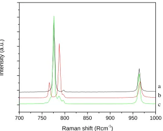
comparison. The spectrum of the machined edge display broadened peaks. The TO mode center frequency is displaced to a higher relative wavenumber while the LO mode center frequency is displaced to a lower relative wavenumber from their crystalline peaks. The broadened displaced TO peak may be attributed to randomly oriented polycrystalline material since the TO mode frequency shifts in this direction for different phonon propagation directions.3 Because of the width of the features, the presence of residual stress cannot be excluded. The TO and LO mode splitting is derived from both the anisotropy of the material, and an electrostatic component of the Si and C atoms. A decrease in the TO-LO splitting may indicate small grain size polycrystalline material which would decrease the long range electrostatic component resulting in an overall decrease in the component of the splitting that is attributed to the electrostatic interaction. In the limit, where the domain size decreases to zero, and the structure resembles a random network, the material is amorphous, all of the Raman modes become active, and the spectrum is expected to resemble the density of states.
The crystal structures of the machined edges were analyzed for a depth of cut of 50, 250, and 500 nm. The surfaces were machined with a sharp tip, and a rake angle of -45°. Raman scattering measurements were obtained from a region of the sample corresponding to the [11 2 0] direction (see Fig. 6). Fig. 10 indicates that the FWHM for
the TO and LO modes is larger for cuts of 50 and 250 nm and decreases when the cut is 500 nm in depth. This indicates a polycrystalline surface layer that may be more disordered or thicker for shallower depths of cut.
As an interesting side note, localized dark spots were observed on the surface of the machined wafer edges. The Raman spectrum from these regions is shown in Fig. 11. The double peak feature is characteristic of sp2 graphitic type C-C bonding. It is possible that the bonding originated from segregation of C from the SiC bulk on the machined surface. Visible Raman spectra of the bulk do not show sp2 graphitic type inclusions indicating that the boding is limited to the surface. We also considered whether the dark spots could be residue left from the diamond tip. However, Raman analysis of machined Si surfaces does not show evidence of sp2-bonded carbon suggesting that the tip is not responsible for the affect.
5.4 Discussion
residual phases. The unloading portion of the load displacement curve does not indicate a pop-out, and the Raman scattering spectrum does not indicate residual metastable phases or polytype transformation. The Raman spectra indicated that the plastic zone of the indentation, although stressed, has a crystalline form. The residual stresses indicate 6H-SiC lattice has not relaxed.
The difference in stress measurements for the TO and LO modes suggests biaxial stress. A larger residual stress is found in the direction perpendicular to the c-axis even though force was applied parallel to the c-axis. This could indicate that the elasticity of the material in the direction parallel to the c-axis is greater than perpendicular to the -axis, and hence, the material can recover to a greater extent in this direction. The broadening in the TO peak can be attributed to a distribution of atomic stresses perpendicular to the c-axis within the laser collection volume. A component of this broadening could also be due to a range of phonon propagation directions on the indented surface.
c
surface layer for larger negative rake angles could be due to a larger degree of compressive stresses generated with larger negative rake angles, or a larger extent of the high pressure phases produced during the machining process. Results have indicated that a larger negative rake angle will create higher compressive stresses at the machining contact interface.4 Thus, a larger extent of the transformed region could be expected for larger negative rake angles.
5.5 Concluding Remarks
UV Raman spectroscopy has allowed for investigation of the surface of indented 6H-SiC (0001), and machined 6H-SiC (0001) wafer edges. The measurements are obtained for probing depths within 35 nm of the materials surface with the 244 nm UV wavelength.
It was found that indentation of 6H-SiC (0001) surfaces produces an inelastic response, and that macro cracking decreases with a decrease in load. UV Raman scattering measurements of a 200 mN load indentation indicate residual biaxial compressive stresses. Stress, and stress gradient are found to be greatest in the center of the indent, and in a direction perpendicular to the c-axis.
5.6 References
1. V. Domnich, Y. Gogotsi, S. Dub, Appl. Phys. Lett. 76, 16 2214 (2000). 2. J. Liu, Y. K. Vohra, Phys. Rev. Lett. 72, (26) 4105 (1994).
3. D.W. Feldman, J.H. Parker, JR., W.J. Choyke, Lyle Patrick, Phys. Rev. 173, 787 (1968).
(a)
-45° rake angle
SiC wafer
0 rake angle
-30° rake angle
0 100 200 300 400 500 600 700 800 900 0
50 100 150 200 250
Loa
d
[
m
N
]
Displacement [nm]
750 800 850 900 950 1000 1050
Intensity
(
a
.u.
)
Raman shift (Rcm-1)
a
b
c
d
Ref. Surrounding Area Edge Center -0.5
0.0 0.5 1.0 1.5 2.0 2.5
P
re
s
s
u
re
(GP
a
)
Position TO mode
LO mode
0 0.1 0.2 0.3 0.4 0.5 0.6
0 0.1 0.2 0.3 0.4 0.5 0.6
700 750 800 850 900 950 1000
In
te
n
s
it
y
(a
.u
.)
Raman shift (Rcm-1)
a b c
750 800 850 900 950 1000
In
te
n
s
it
y
(
a
. u
.)
Raman shift (Rcm-1)
a b c
750 800 850 900 950 1000
Inten
s
it
y
(a.u.)
Raman shift (Rcm-1)
FIG 10: UV macro Raman scattering spectra of machined 6H-SiC edges for machining depths of (a) 50, (b) 250, and (c) 500 nm depth of cut per revolution. The spectra were obtained with the incident light along the [11 2 0] direction of the wafer.
600 800 1000 1200 1400 1600
In
te
n
s
it
y
(a
.u
.)
Raman shift (Rcm-1)
b a
6. UV Raman Scattering Analysis of Machined β-Si3N4
Jennifer J.H. Walter1, Mengning Liang1, Xiang-Bai Chen2, Leah Bergman2, John A.
Patten3, Robert J. Nemanich1
1
North Carolina State University, Raleigh, NC 27695
2
University of Idaho, Moscow, ID 83843
3
University of Western Michigan, Kalamazoo, MI 49008-5314
6.1. Experimental Summary
This study addresses the properties of precision-machined polycrystalline β-Si3N4
surfaces. Prior research has reported ductile surface properties produced from
indentation and grinding of β-Si3N4.1, 2 It is possible that the pressure-induced plasticity
is similar to that found in Si with its origin in a high pressure phase transformation to a
metallic phase. Preliminary diamond anvil cell experiments of β-Si3N4 indicate
low-energy X-ray diffraction peaks at pressures between 20 and 35 GPa suggesting an
unidentified high-pressure phase.5 Raman scattering of the ductile surfaces indicate a
residual layer of an amorphous phase. This amorphous surface layer may be the relaxed
phase of a high-pressure metallic phase. We have used wavelength dependence Raman
spectroscopy to probe the depth dependence of the residual amorphous zone left from
machining. The short absorption depth of UV light allows for accurate probing of the
surface, and the transparency to visible light allows for analysis of the bulk material.
6.2 Experimental Details
The β-Si3N4 surfaces were prepared first by grinding and then machining over the ground
surface. The machining was employed for depths of cut of 500 nm, 5 µm, and 10 µm. Si
showed a peak at 520 Rcm-1. Because of the slow machining speeds employed, we
expect that there was a minimal increase in temperature. Tool wear could influence the
analysis by changing the sharpness of the tip with use. However, for the limited
machining distances in these tests we expect that wear was not an issue.
The Raman scattering experiments were performed with two spectrometers, one with
macro and the other with micro focusing optics. In the macro system, a ~45°
backscattering geometry was employed and the laser was focused to 100 µm spot on the
sample. The Raman experiments were performed with the 244 nm UV line of a
frequency doubled argon ion laser (Coherent Inc.), and the scattered light was focused
onto the entrance slit of a triple spectrometer (Spex Triple Mate 1877). In the micro
Raman system, a 180° backscattering geometry was employed and the laser light was
focused to a spot size of ~2 µm on the sample. The Raman experiments were performed
with the 244 nm UV line of a frequency doubled Ar ion laser (Lexel Inc.) and the 325 nm
UV line wavelength of a HeCd ion laser (Kimmon Electric Inc.), and the scattered light
was focused onto the entrance slit of a triple spectrometer (Dilor). For both systems,
CCD detection was used to collect the spectra. The probing depth into polycrystalline β
-Si3N4 with a 244 nm line is ~1.4 µm (the values are calculated for the depth in which the
intensity of the light is 37% of the incident intensity).
6.3 Results
A SEM image of a chip removed from the surface during machining is presented in Fig.
was bent and distorted without fracture indicating that the material removed from the
surface is ductile.
The spectra presented in Fig. 2 represent data collected with an excitation wavelength of
244 nm and were obtained from the surface of machined β-Si3N4, at depths of cut of 500
nm, 5 µm, and 10 µm. The Raman scattering spectra of the machined surfaces show
broad features, and the sharp peaks associated with crystalline structures are absent. This
broadening can be related to the broadened phonon density of states representing an
amorphous structure. The broadened density of states contains two broadened peaks
centered at ~400 and ~900 Rcm-1.6 In comparison, the ground surfaces exhibit crystalline
peaks with some evidence of an amorphous component.
Fig. 3 presents the Raman scattering spectra of the machined β-Si3N4 surface for a 5 µm
depth of cut and incident wavelengths of 514.5, 325, and 244 nm. The 514.5 nm visible
Raman scattering spectrum indicates sharp crystalline peaks. In the spectrum obtained
with the 325 nm incident wavelength, the peaks are slightly broader, but the broad
background. The spectrum obtained with the 244 nm incident wavelength indicates a
completely broadened spectrum. The results indicate that the bulk of the material is
crystalline indicated by the sharp peaks and the surface is amorphous indicated by the
broadening.
The Raman scattering spectrum of the chips removed from the surface is shown in Fig. 4.
that the chips are amorphous. There is some extent of crystalline peaks observed in the
micro Raman scattering spectrum indicating that the power density produced by the small
spot size in micro Raman scattering spectrum was high enough to heat and crystallize the
chips.
6.4 Discussion
Machining for depths of cut on the nm and µm scale resulted in a ductile surface and
ductile material removal. Raman scattering measurements of the ductile, machined
surfaces indicated an amorphous layer. The spectra from the grounded regions indicated
crystalline peaks, with some amorphous component. It is possible that the amorphous
remnants result from surface polishing of the material before grinding or that these
amorphous remnants are a direct result of the grinding. The sharp peaks in the visible
Raman spectra of the machined surfaces indicate that the bulk of the material is
crystalline, and the broadened peaks in the UV spectra indicate that the surface is
amorphous. The Raman scattering spectra of the debris removed from the surface during
machining indicate that the chips are also amorphous. Although it has been demonstrated
that while machining a higher degree of compressive stresses while machining are
generated within the chip,7 it is expected that the material removed from the surface
should has a similar structure of the surface.
A direct crystalline to amorphous transformation is not expected at room temperatures.
Therefore, the amorphous layer may result from relaxation from a high-pressure metallic
6.5 Conclusions
It has been found that β-Si3N4 can be machined in a ductile regime for cutting depths on a
scale of µm and nm, and is evidenced by a smooth surface finish and ductile chips
removed during machining. The machined surfaces indicated a residual amorphous layer
where the extent of the amorphous layer is limited to the materials surface. The residual
amorphous phase may result from relaxation of a high-pressure metallic phase. X-ray
diffraction peaks indicate a pressure phase at ambient temperature. The
high-pressure metallic phase could explain the origin of the ductile response observed on the
6.6 References
1. J. Patten, Advances in Abrasive Technology III (Japan Society of Abrasive
Technology, Tokyo, 2000) p. 87.
2. C. Ullner, J. Beckmann, and R. Morrell, J. Eur. Ceram. Soc. 22, 1183 (2002).
3. J.J. Gilman, Philos. Mag. B 67, 207 (1993).
4. V. Domnich, Y. Gogotsi, Experimental methods in the physical science 38, 355 (2001).
5. C. Ullner, J. Beckmann, and R. Morrell, J. Eur. Ceram. Soc. 22, 1183 (2002).
6. N. Wafa, S.A. Solin, J. Wong, and S. Prochazka, J. Non-Crys. Solids 43, 7 (1981).
7. J. Morris, D. Callahan, J. Kulik, J. Patten, and R. Scattergood, J. Am. Ceram. Soc. 78,
500 600 700 800 900 1000 1100 1200
In
tens
it
y
(a.u
.)
Raman shift (Rcm-1)
a
b c
d
FIG 2: UV Raman scattering spectra of (a) grounded and machined (b) 5 µm (c) 10 µm
500 600 700 800 900 1000 1100 1200 1300
In
te
ns
it
y
(a
.u
.)
Raman shift (Rcm-1)
c b a
FIG 3: (a) Macro Raman scattering spectrum of the bulk of machined β-Si3N4 is shown