1
New superconductivity and theoretical study on a new phenomenon of
energy source with assistance of initial experiments
Author detail Name
: Shinichi Ishiguri
Affiliation
: Nihon University
1-2-1, Izumi-Cho, Narashino City, Chiba, 275-8575 JAPAN
TEL
: +81-47-474-9143
: ishiguri.shinichi@nihon-u.ac.jp
Abstract: We previously reported new superconductivity produced by an electrostatic field and a diffusion current in a semiconductor without refrigeration. In particular, the superconductivity was investigated theoretically and confirmed experimentally. Here, we determine that the derived superconducting quantum state can be reproduced in a capacitor. When circuits are formed with this new-type capacitor and diodes, a magnetic field is applied to the diodes’ depletion layer. The depletion layer is biased because of the conversion from the magnetic-field energy to electric-field energy, resulting in the diodes’ spontaneously emitting a current. Thus, the new-type capacitor is charged using no other energy source. This new phenomenon is described theoretically with assistance of initial experiments.
Keywords: new superconductivity, condensation state, new electric field, current emission, new type capacitor, Aharonov–Bohm effect, new energy source
1.
Introduction
High-temperature superconductors have been investigated at many places. This reason is that, in condensed matter physics, physical aspects are unique in addition to their high critical temperatures.[1-8,14] However, in considering applications, the fact that the refrigeration is needed must be disadvantage. Thus we need to obtain no refrigeration superconductors. Recent studies revealed that a system, wherein electrostatic fields and a diffusion current are applied to a doped semiconductor, exhibits the superconductivity generation, quite different from its conventional counterpart [9, 10]. By this conduction, internal electric fields become zero because of the cancelation of the ohmic electric and the electrostatic fields. However, the current does not become zero because the diffusion current is carried by a force proportional to the gradient of the carrier concentration. In our previous studies [9, 10], we investigated this new superconductivity both theoretically and experimentally. Thus, we produced the following:
(1) configuration of the new device based on this superconductivity;
2 (2) new theoretical interactions between electron pairs and the persistent current;
(3) experimental results that describe zero resistance and the Meissner effect (4) a method to reproduce our experiments.
The global industry currently faces a major energy challenge, which is being managed using solar cell technology [11] and energy storage devices [12]. In this study, based on the new superconductivity, we produce spontaneous current emission derived from magnetic-field energy. In particular, applying an electrostatic field and a diffusion current to a doped semiconductor clearly creates a new temperature-independent quantum state, which forms internal inductances with magnetic-flux quanta. The wave function of the quantum state can be reproduced in a capacitor based on the Aharonov– Bohm effect [13]; thus, we derive a new-type capacitor containing a persistent current. By constructing an electric circuit that incorporates this new-type capacitor and some p–n diodes, the magnetic-field energy produces a bias voltage across the diodes because of its conversion from magnetic-field energy to electric-field energy. As a result, a spontaneous current is emitted from the diodes into the new-type capacitor. In this way, energy can be stored without using batteries. Therefore, our present results potentially contribute to the solution of the energy problem. We study this theoretically with assistance of initial experiments.
The configuration of the present paper is started by the reviews of the new superconductivity and the reproduction of wave function of the superconductivity to a condenser. Considering these facts, we will describe the diodes’ spontaneous current emission as an original point. Please note that the word “new phenomenon” implies the new superconductivity or the diodes’ spontaneous current emission, i.e., at both cases, we referred as “new phenomenon” in this paper.
2.
Review of new superconductivity
2-1 Review of our previous reported theory
Principles of the proposed device
3 Fig. 1: Schematic of the voltage generation in a semiconductor by a diffusion current (source indicated at right). The graded coloring in the doped semiconductor implies the gradient of the carrier concentration, which causes the carriers to diffuse.
Fig. 2: Schematic of the new superconducting device. Two capacitor pole plates are located above and below the semiconductor. The capacitor generates an electrostatic field proportional to the ohmic field.
Outline of the theory
Here, we summarize the theory presented by Ishiguri [9–10].
Point 1: New electric field generated from an electron: new interaction between two electrons
A particular electron concentration, which depends on the characteristics of our device, results in an electrostatic potential. By solving Poisson’s equation for the electrostatic potential between two electrons, we obtain the following interaction potential Vα:
𝑉 =−𝑛0𝑘𝐵2𝑇2 𝑞𝜀𝐸𝑖2 exp (
𝑞𝐸𝑖
𝑘𝐵𝑇𝜉) (1)
where kB, T, ε, Ei,q, n0, ξ, and i denote Boltzmann’s constant, the temperature, the permittivity, the
constant local electric field, the electric charge, a constant, a relative coordinate, and a lattice index, respectively. The Coulomb repulsive interaction is also determined by Poisson’s equation, but it does not appear on a macroscopic scale.
RI I
Doped semiconductor
4 A new electric field can be obtained from eq. (1):
𝐸 = − exp ( 𝜉) (2)
This electric field has features of both an electrostatic field and one associated with a current. To ensure that Em(ξ) is not divergent, we must define a circle integral of Em(ξ), i.e., a voltage. Note that only at ξ = 0, the circle integral is undefined, because the normal ordinate of the relative coordinate must be an edge of the integral, and this normal ordinate should not be a part of the integral’s path. This exception allows Em to have both a static component and a component associated with a current. The
spatial integral of Em results in a negative voltage (i.e., the new electric field), whose existence is
demonstrated by experimental results [10]. Hereafter we refer this new type electric field as coiled electric field.
Point 2: A critical current exists
The above-mentioned attractive interaction potential Vα can cause two electrons to approach each other,
until they are only a lattice diameter apart. At this stage, the total energy H of the systemis expressed as follows:
H = 𝑉 + 𝑉 + 𝑉,
𝑉 + 𝑃 = 0. (3)
Here, V is the spin magnetic potential, given by
V = − ħ| | (4)
where m and zm denote the electron mass and the microscopic relative coordinate, respectively. In eq.
(3),P and Vp represent the kinetic and zero-point energies at the lattices, respectively, and Vp is
expressed as follows:
𝑉 = ħ𝜔𝛿(𝜉) (5)
where ω and δ are the angular frequency and a delta function, respectively. The following conditions should be satisfied for the combination of two electrons:
|𝑉 (𝜉 = 0)| ≥ 𝑉 and (6-1)
|𝑉| ≥ 𝑃 (6-2)
When eq. (6-1) is satisfied, both electrons are located at the zero-point of the lattice. When eq. (6-2) is satisfied, the microscopic relative distance, zm (i.e., the coherence), is to be calculated as follows:
𝑧 ≤ 1.0 × 10 [𝑚] (7)
5 remains, and the total energy becomes negative; a collision between the two electrons is perfectly inelastic, and the two electrons therefore combine. Equation (6-1) can also be rewritten as follows
𝑛 𝑘 𝑇 ≥ 𝜀ħ𝜔𝐸 (6-1)
This condition indicates that the local electric field Ei is at its maximum value. The electrostatic field
is proportional to the Joule electric field, which is in turn dependent on the current density. Therefore, a critical current exists, which corresponds to this maximum. Moreover, as described in eq. (7) the coherence of the pair is extremely short.
Point 3: The Bose–Einstein (BE) condensation of electron pairs is temperature-independent, since locally combined pairs do not collide
More information regarding this point is offered by Ishiguri [9]. However, some important equations are presented below.
The Hamiltonian of a pair in terms of center-of-mass-motion is
H = − (ħ ) + 𝑈. (8)
The potential U indirectly implies the electrostatic potential of two electrons:
U = − ∫ 2𝑞𝐸 𝑑𝑥 = −2𝑞𝐸 (𝑥 − 𝑥 ), (9)
where x1 and x2 denote the positions of the two electrons.
The location at the identical lattice of the two electrons, i.e., the local combination of the two electrons at the lattice implies equation x1=x2. Moreover, from the Hamiltonian, the following wave function is
derived. Note that at the moment of the identical location, the potential in the Hamiltonian transforms to the eigenvalue (i.e., the kinetic energy), which arises from the local electric field Ei. Therefore the
distribution of a local electric field Ei within a lattice vanishes.
𝜑 = 𝛾exp [ ħ 𝑗𝑥], (10)
where μ denotes the mobility of the pair at a lattice. If we use the following equations,
= 𝐸 , (11-1)
𝜎 =
△ / 𝜇, (11-2)
Then the wave function derives as
𝜑 = 𝛾exp [ ħ 𝑥𝐽△ /], (13)
where σi , △Vi, and J denote the conductivity at a lattice, variation quantity of volume with respect to
6 Eq. (11-1) indicates the proportion of the Joule electric field and the electrostatic field at a lattice-scale level. After substituting eq. (11), the mobility (i.e., conductivity) and local electric field Ei vanish.
The above wave function is indexed by i, and a wave function at the next lattice does not interact the wave function indexed by i. This reason is that the distance between two neighboring lattice is much larger than the coherence of the two electrons.
An entire wave function is represented as follows:
ψ = ∏ 𝜑 = 𝛾 exp [
ħ 𝑥 ∑ 𝐽 ] (14)
When we imagine the index i as infinite, and the semiconductor volume as constant, the lattice volume converges to the differential dV. Thus, the concept of a countable lattice loses its meaning, and
a macroscopic continuous body appears.
→ η exp
ħ 𝑥 ∫ 𝑑𝑉] = 𝜂exp [ ħ 𝑥𝑎 ∫ 𝑑𝑆 = 𝜂exp [ħ 𝑎𝑗𝑥] (15)
From this function, the wave number is
K =
ħ 𝑎 = 𝑎 (16-1)
where M denotes the spin magnetic moment of an electron (which is obtained from the Dirac equation), and a is the constant coherence. The spin magnetic moment can be correlated to the combination energy (i.e., the spin interaction) from eq. (4) as
K =
√ 𝑉 ≤ 0 (16-2)
where V denotes the spin interaction given in eq. (4)
In eq. (16-2), current I is independent of the collision time; therefore, it is a superconducting current. Moreover, the wave number in this equation is uniform and not related to space; thus, all quantum states converge to a single state, and complete Bose–Einstein (BE) condensation occurs.
2-2. Review of our previous experiments
Method
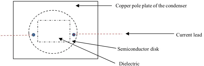
For detailed information on the experiments, we refer the reader to the main part of the article, which includes a description of the experimental setup and the method for the reproduction of the experiments [10]. Nevertheless, important figures are presented here. Figure 3 shows the schematic of the cross section of the new superconducting device. The device comprises the semiconductor, the condenser pole plates, and the dielectric between the semiconductor and the pole plates. Dehydrated wood was used as the dielectric material. The current leads to the semiconductor were attached by a
i Vi/
7 supersonic-wave soldering iron. By altering the direction of the supplied current, we confirmed that the current-lead connections were ohmic contacts. The semiconductor was an n-type silicon wafer, with electrical resistance, radius, and thickness of 550 Ω, 62.5 mm, and 0.6 mm, respectively. The critical current was less than 10 μA. In this figure, a voltage source is used to charge the condenser pole plates, i.e., it is connected to the condenser pole plates and the current source that provides the diffusion current is connected to the current leads of the semiconductor. Moreover, the dielectric material prevents the flow of current from the current source to the condenser pole plates. The top view is shown in Fig. 4. Note that we devised the method for obtaining the area to attach the current leads. As an experimental method, after the voltage source (1V) is applied to the copper pole plates of the condenser and the relatively large diffusion current (i.e., mA order) is supplied to the current leads by the current source, the voltage and current sources are simultaneously switched off. During the switching off process, there is a moment when the decaying current equals the critical current. At this moment, the new phenomenon occurs. Note that the net current after the transition is not zero, which forms a circle current in semiconductor as the persistent current as indicated eqs. (15)-(16). This is demonstrated by the statistic magnetic field application as discussed later.
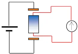
Fig. 3: Schematic showing a cross-section of the novel superconducting device. The voltage source is connected to the condenser pole plates to generate a static electric field and the current source is connected to the current leads to supply diffusion current. The dielectric material prevents the flow of current from the current source to the condenser pole plates.
Fig. 4: Schematic of the new superconducting device as viewed from above.
Wood (dielectric)
n-type semiconductor disk
Condenser pole plate (copper) To voltage source
6.
5
m
m
current lead
Copper pole plate of the condenser
Semiconductordisk
Dielectric
8 Zero resistance and the Meissner effect
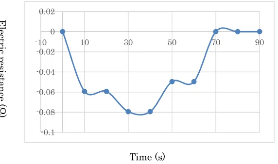
In Fig. 5, the results from the experiments are shown. At first a negative electric resistance was obtained, i.e., the energy was generated and a new electric field, as described by Eq. (2), appears. At 65.8 s, the resistance became almost zero. Before applying the electrostatic field and diffusion current, resistance of the semiconductor was about 550 Ω and after applying the electrostatic field and the diffusion current, the resistance became about 10-5 times smaller.A positive value on the order of
0.01Ω was disregarded as noise, which may have arisen from sources such as the contact resistance (the negative resistance is not included). When applying static magnetic fields, a dc current was induced from the current leads. This current emission implies that the Meissner effect generated a shield current in the sample, and its current was affected by the static magnetic field, i.e., it was a superconducting current. This is interpreted that the persistent current exists and this current functions the shield current.Note that this superconductor has no critical temperature. Thus we cannot employ the conventional measurement of the Meissner effect, i.e., zero-field-cooling and field-cooling. However the above dc application of magnetic fields induces the dc current, which is driven by the Lorentz force. This implies that the superconducting electrons exist, and current density of these superconducting electrons gives the London Equations [16]. The measurement of the Meissner effect, i.e., the broken symmetry of the gauge is essential of a superconductor [17]. In this case, we employed the magnet smaller than the semiconductor disc. When the static magnetic field was applied in the vicinity of an attached point of the current lead, the current was induced as plus direction, while that magnet was applied in the vicinity of the other attached point, the current was induced as minus direction. Those results are shown in Figs. 6 and 7.
Fig. 5
:
Electrical resistance as a function of time. The measurements began immediately after the voltage and current sources were turned off. A negative electrical resistance was initially observed, which generally implies that energy is generated rather than consumed. In this study, this observation implies the existence of a coiled electric field-0.1 -0.08 -0.06 -0.04 -0.02 0 0.02
-10 10 30 50 70 90
E
le
ct
ric
re
sis
ta
n
ce
(Ω
)
9 as described in Section 2. At 68.5 s, the electric resistance returns to approximately zero.
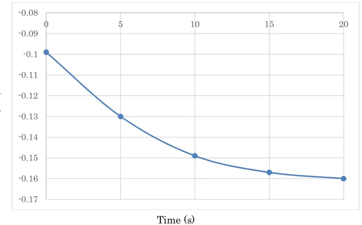
Fig. 6: As shown in Fig. 4, there are two attached points of current reads to the semiconductor. After the separation
of the condenser pole plates and semiconductor having the current leads and when applying a small magnet in the vicinity of the point of a current lead, voltage, .i.e., current was induced. This implies that superconducting shield current from the Meissner effect was observed.
Fig.7:
The magnet was applied to the other point of a current lead. In contrast to Fig. 6, the induced voltage, i.e., current was induced as the reverse direction.-0.17 -0.16 -0.15 -0.14 -0.13 -0.12 -0.11 -0.1 -0.09 -0.08
0 5 10 15 20
0.08 0.09 0.1 0.11 0.12 0.13 0.14 0.15 0.16
0 5 10 15 20
10 3. Theory of the present study
The condensed wave function in the new superconducting state is expressed from eq. (15), as follows [9]:
𝜓 = 𝜂exp ( ħ 𝑗α), (15)
where m, a, q, and Ip are the electron mass, constant coherence, electric charge, and persistent current,
respectively.
From the existence of the current Ip, we introduce a magnetic flux given by
𝛷 = 𝐿 𝐼 (17)
In addition, the vector potential Aφ is defined in cylindrical coordinates as
𝐼 = (18-1)
= (18-2)
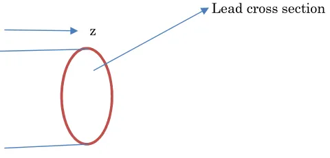
Note that, we mean that the cylindrical coordinates are rotation φ along the wire cross-section and the direction z along the current lead as illustrated in Fig.8
Fig. 8: the image of the cylindrical coordinates. The z-axis is along the current lead. Concerning the cross section of the lead, circle red line implies φ-axis
Thus, eq. (15) becomes
𝜓 = 𝜂exp (ħ𝑗 ∫ 𝐴 𝑑𝛼). (19) By considering the phase, the following equations can be derived:
𝜑 = ħ 𝛼 = ħ ∫ 𝐴 𝑑𝛼 = ħ 𝛷, (20-1)
φ = 2𝜋𝑛 . (20-2)
Therefore, we obtain the following magnetic-flux quanta:
11
𝛷 = 𝑛 . (21)
We must review the characteristics of condensed toroid and condensed solenoid: from the complete Bose–Einstein condensation, the electron pairs along each coil element of the condensed toroid or solenoid move with the same rotational velocity and through the same angle. Therefore, each moving φ-direction electron pair experiences attractive Lorentz forces from the nearest moving pair of electrons. In other words, all electron pairs move collectively along φ-direction. Equation (19) refers to the solenoid condensed state, where the electron pairs are condensed and generate magnetic flux, while the toroid collapses entirely. In view of the magnetic-field energy, the condensed toroid has less energy than that of the solenoid condensed state [15]. The magnetic field vector in this paper is along z-direction.
We claim that, in general, if another path, such as an electric circuit, is connected to the superconducting state (i.e. the condensed solenoid), their electron pairs are diffused along the attached path, forming spiral with combine of the interaction with the magnetic field. These electron pairs are not destroyed because of the strong combination energy higher than that of the room temperature [9]. However, because of the Aharonov–Bohm effect, the condensed toroid will be formed along the new electric circuit by the eq. (22) because some parts of the electric loop away from the connections maintain the condensed solenoid. The condensation collapse because of the self-field and the quantum state changes to another condensed form, i.e., based on gauge symmetry, the phase of the wave function changes because of the self-field A [13]:
𝜓 = 𝜓 exp
ħ 𝑗 ∫ 𝐴⃑ ∙ 𝑑 𝑟⃑ = 𝜂exp [ ħ ∫ 𝐴 𝑑𝛼 + ħ ∫ 𝐴⃑ ∙ 𝑑𝑟⃑ 𝑗]. (22)
Based on the consistency of the two boundary integrals, the first and the second terms of eq. (22) are combined to form circular integrals as follows:
𝜓 = 𝜂exp (
ħ 𝑗 ∮ 𝐴⃗ ∙ 𝑑𝑟⃗) (23-1)
θ = ħ𝑗 ∮ 𝐴⃗ ∙ 𝑑𝑟⃗ and (23-2)
θ = 2𝑛 𝜋 (23-3)
Thus, we obtain
𝛷 = 𝑛 (24)
Because the magnetic fields are along the z-direction (i.e., along the current lead), the above procedure indicates that a condensed quantum toroid [10] is produced along the circuit.
Let us precede to original points of the present paper:
We consider a capacitor to be connected to the superconducting device. Similarly, some pairs are diffused to the capacitor in the process of forming the condensed toroid. This diffusion to the
12 because of the strong pair combination energy, which is higher than that at room temperature [9]. In this case, the basis of the gauge symmetry results in
𝜓 = 𝜓 exp
ħ𝑗 ∫ 𝐴⃑ ∙ 𝑑 𝑟⃑ = 𝜂 exp ħ ∫ 𝐴 𝑑𝛼 + ħ ∫ 𝐴⃑ ∙ 𝑑𝑟⃑ 𝑗 = 𝜂 exp ħ ∫ 𝐴 𝑑𝛼 +
ħ ∫ 𝐴 𝑑𝛽 + ħ∫ 𝐴 𝑑𝛽 𝑗 = 𝜂 exp ħ ∫ 𝐴 𝑑𝛼 + 2 ħ ∫ 𝐴 𝑑𝛽 𝑗 = = 𝜂𝜓2𝜓 (25)
In contrast, eq. (25) implies that the vacancy between condenser pole plates prevents the formation of the circle integral; because the self-field formed in the device, the first solenoid condensate collapses but the new solenoid condensates are reproduced eventually. Therefore, the capacitor exhibits the same wave function as eq. (19). That is, the persistent currents form in both the condenser pole plates. Note that the vacancy between the pole plates does not have the persistent current. The diffused electron pairs form a condensate at the capacitor, which yields a magnetic field in the capacitor pole palates. Using eqs. (18-1), (17) and (24), the magnetic field in cylindrical coordinates is expressed as
𝐵 = [ ] = 𝑛 , (25)
where rpc denotes the radius of the elemental coil of the magnetic-flux quantum in the capacitor.
Therefore, a uniform magnetic field is distributed along the z-axis, and the energy u is added to the capacitor pole plates.
The energy is given by
u = ∫ 𝑑𝑣 and (26)
𝑢 = ( ) ∭ 𝑑𝑟𝑑𝑧𝑟𝑑φ = ( ) log ( ), (27)
where d and rc are the width and radius of the cylindrical capacitor pole plates, respectively.
Next, we separate the capacitor from the circuit. Because the capacitor has an identical wave function as eq. (19), the condensed solenoid is formed. this specific capacitor is referred as the “new-type capacitor.” Furthermore, the capacitor must be shorted to form the toroid. However, because the two pole plates of the capacitor have the same negative charge from electron pairs, a discharge does not occur.
After the new-type capacitor is shorted electrically, it is connected to a diode, thereby forming another circuit. The depletion layer of the diode has an internal capacitor. Thus, basically, although the same process is followed, the calculations are derived for the initial state.
13 increase because of the self- magnetic fields. When the diode is shorted and reconnected to the capacitor, the circle motions cease and these electrons and holes move to the depletion layer such that the increased magnetic field energy reduces at the edges. Thus the element coils in the depletion layer edges locally discharge a diffusion current, which contains the electrons and holes at the edges of the depletion layer. Thus, in the depletion layer, the ohmic diffusion current and an electrostatic field Ei
originating from the diffusion potential produce a transient-state potential, i.e., the coiled electric field. In short,after the initial state, the above magnetic-field energy (27) is transformed into electric-field energy.
u = −q𝑣 + 𝑞𝑣 ≈ −𝑞𝑣 (28)
where vαn and vαp are the voltages of the coiled electric field (1-2) because of electrons and holes,
respectively.
𝐸 = − exp ( 𝜉) (29-1)
𝐸 = − exp ( 𝜉) (29-2)
where eqs. (29-1) and (29-2) denote the coiled electric fields for electrons and holes (i.e., transient electron pairs and hole pairs), respectively; eq. (29-2) decays. Thus, the net electric field is approximated in eq. (29-1) by the transient electron pair. This electric field results in the motion of the holes and produces a spontaneous current; this current leads to the storage of energy in the capacitor. Equation (29-1) expresses the energy distribution at the depletion layer edge forming a coil and works on normal holes.
In the charging process, a current flows from the holes, temporarily. However, as the time for which the current flows increases, the probability that the holes will recombine with the electrons in the diode also increases. This implies that the number of holes is gradually reduced with time as the current flow. However, the number of holes in the diode is finite. Thus, the lifetime of the current emission is defined. Note that to store energy, the following condition should be satisfied:
u − 𝑅 𝐼 𝑡 ≥ 0 (30) where RE and t denote the effective internal resistance for the normal current Is and time, respectively.
When this condition is satisfied, the difference is positive and energy is stored. In addition, given the above condition, Is is the normal current from the normal holes affected by the transient electron-pair
electric field (29-1), and Ip in eq. (27) is the persistent current derived from the electron pairs motion.
This persistent current forms loops as magnetic flux quanta in the capacitor; thus, this persistent current differs from Is. The current Is flows in the z-direction, whereas the persistent current Ip flows
in the φ-direction.
14
Δ 𝐶 𝑣 = u − 𝑅 𝐼 𝑡 = ( ) log ( ) − 𝑅 𝐼 𝑡 (31)
where v and Cs are the capacitor voltage and the capacitance, respectively. In addition, the left-hand
energy gradually decays with time t.
4. Results and discussion
From the previous section, we numerically calculated the dependence of capacitor voltage for time. The parameters are listed in Table 1.
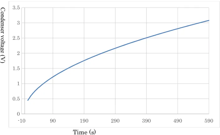
Fig. 9 shows the condenser charge voltage for Is=10-7 A. As shown, the voltage increases as function
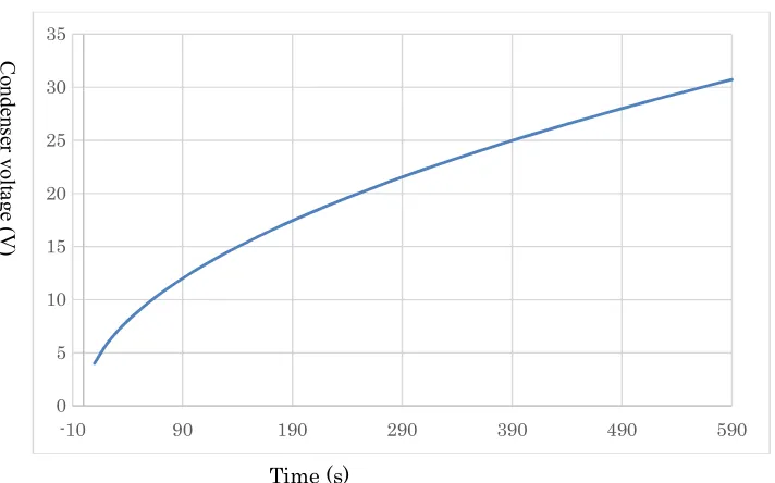
of time. Fig . 10 indicates the condenser voltage for Is=10-6A. Compered with Fig. 9, the charge
voltage increases. The current Is is the induced current. Thus, it is assumed that it determined by the number of the diodes, which are connected by series and parallel. The larger the number of the series and parallel diodes, the higher the induced current Is is. In this case, however, the net volume of the device increases. Moreover, as shown in these figures, the charge energy does not diverse. That is, initially the gradient of the curve is high but the gradient of the curve becomes moderate with time. Therefore , at the steady state, the voltage increase of the capacitor ceases.
Fig. 9 The 1 μF condenser charge voltage for Is=10-7 A. Initially the gradient of the curve is high but
the gradient of the curve becomes moderate with time. Therefore, at the steady state, the voltage increase of the capacitor ceases.
0 0.5 1 1.5 2 2.5 3 3.5
-10 90 190 290 390 490 590
C
on
de
ns
er
v
olt
ag
e (
V
)
15
Fig. 10 The 1μF condenser charge voltage for Is=10-6A. With increase of the induced current Is, the
condenser charge voltage also increases, compared with Fig. 9.
Table 1 The parameters of the numerical calculation
a 10-10 m
Ip 10-6 A
RE 8 × 10 𝛺
rc/rpc 1.1
Cs 10-6 F
d 4 × 10 𝑚
As discussed previously, the parameter a is the constant coherence, which is estimated by 1Å. The current Ip is the persistent current less than the critical current 10μA. The resistance RE is the net
internal resistance of the diodes and the voltmeter. These diodes were biased reversely. Thus, impedance RE is large in addition to that of the voltmeter. The parameter d was determined from the
typical length of the depletion layer of a diode. The Ratio rc/rpc is almost the value 1 but was determined
by the fact that the first and second terms of eq. (31) have same ordering value, i.e., it was obtained such that eq. (31) gains its meaning. The capacitor was a normal ceramic condenser which can be easily purchased.
0 5 10 15 20 25 30 35
-10 90 190 290 390 490 590
C
on
de
ns
er
v
olt
ag
e (
V
)
16
5.
Energy source experiments
Method and notation
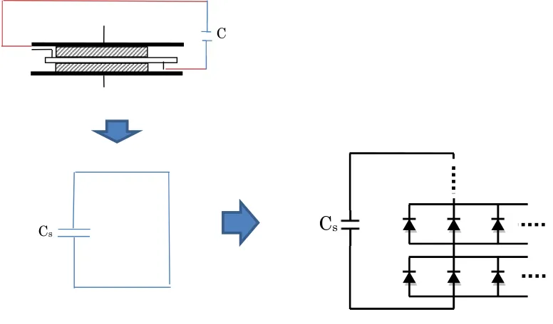
Because the increase in voltage across the new-type capacitor plus diode is relatively small, we demonstrate the voltage increase across the new-type capacitor connected with several diodes.In this experiment, the 40 diodes are normal silicon-based p–n diodes; ten of these are connected in series, whereas four diodes are connected in parallel. The capacitors are normal ceramic capacitors with capacitances of 1 and 10 μF. The DMM (ac line input: 100 V, 50/60 Hz) used in this study was purchased from Iwatsu Electric Co. Ltd. As shown in Fig. 11, first, the normal condenser is made to the superconducting condenser by connecting to the superconducting semiconductor. Then this new-type capacitor must be shorted electrically before connecting the diodes. After the capacitor is connected to the diodes, the diodes are also shorted. Next, the capacitor is connected to the diodes. An important point is that the diodes were biased reversely. Thus, we need to be careful of their direction. Note that the claim of this paper is completed in theory section. Thus, these experiments exist merely for assistance of this claim. As you know, statistical experiments will be needed in the future works
Fig. 11: Schematic procedure of the experiments: First, a normal ceramic condenser C is connected to the superconducting semiconductor. By this conduction, the condenser becomes the new type condenser Cs whose pole plates have the superconducting persistent current. Next, this new type
condenser is connected to some normal pn diodes. C
C
s17 Result and discussion
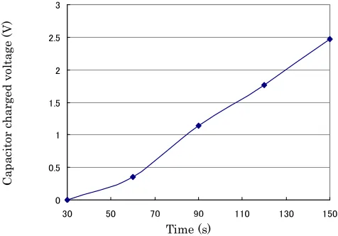
As shown in Figs. 12 and 13, the voltage across the new-type capacitor increases. Moreover, in Fig.13, after 90 s, the voltage gradient becomes moderate. This implies that the theoretical eq. (31) is satisfied. In eq. (31), after sufficient time, the energy increase becomes zero, and the capacitor voltage becomes constant. In Fig.12, we measured the condenser voltages by auto -range of the meter. This conduction results in that the voltage increase stops at the moment when the meter varies the range. That is, at 5.0 V of the voltage in the condenser, the voltage stops in meter’s varying the range.
Fig. 12: Experimental result: Voltage of capacitor charge vs. time. Capacitance of the new-type capacitor is 1 μF. The circuit consists of normal p–n diodes and the superconducting capacitor. No other batteries are used.
Fig. 13: Experimental result: Voltage of capacitor charge vs. time. The capacitance of the new-type capacitor is 10 μF. The other conditions are the same as those in Fig. 12.
0 0.5 1 1.5 2 2.5 3
30 50 70 90 110 130 150
Time (s) C ap ac it or c h ar ge d vo lt ag e (V ) 0 50 100 150 200 250 300 350
30 50 70 90 110 130 150
18 In Fig. 14, we offer a video of the energy-charge process using the new-type capacitor. First, a brown capacitor,.i.e., the new type capacitor is being shorted. Next, this capacitor is connected to 40 diodes. A capacitor voltage increase in the DMM is observed. Next, the capacitor is shorted again and reconnected to the 40 diodes. Then, the capacitor regains energy. Note that no energy source is applied.
https://www.dropbox.com/s/son8lgzsiprp3m5/experiment%20renew%20002.MTS?dl=0
Fig. 14: Video of the process, through which the new-type capacitor gains energy without using an external energy source.
6.
Conclusion
In this paper, based on a newly discovered superconductivity, we report a new energy source. In our previous studies, we revealed that applying an electrostatic field and a diffusion current to a doped semiconductor produces the new superconductivity, which forms internal inductances with magnetic-flux quanta. This superconductivity was reviewed in this paper. That is, electron pairs, superconducting current and BE condensation are produced theoretically. Furthermore, zero resistance and the Meissner effect were confirmed experimentally
Based on the Aharonov–Bohm effect, the quantum state can be reproduced in a capacitor, thereby leading to a new-type capacitor. By using an electric loop comprising the new-type capacitor and diodes, the magnetic-field energy creates a bias voltage across the diodes because the magnetic field energy is converted to the electric field energy. As a result, the diodes spontaneously emit currents that accumulate in the new-type capacitor. In the numerical calculations, we saw that the charged voltages of the condenser increases with time and that the gradient of the curves become moderate with time. From the result of this, it is necessary to make the number of the diodes increase to gain more energy. Thus, integrated circuit technology allows very high energies to be quickly accumulated in a capacitor.
References
[1]. P. W. Anderson, et al, J. Phys.: Condens. Matter Vol. 16, No. 24, (2004) R755 [2]. P. A. Lee, et al, Rev. Modern Phys., Vol. 78, (2006) 17
[3]. M. Ogata, H. Fukuyama, Rep. Prog. Phys., Vol. 71, (2008) [4]. M. Azuma, et al, Phys. Rev. Lett, 73 3463 (1994)
[5]. F. C. Zhang, T. M. Rice, Phys. Rev., Vol. B 37, (1988) 3759
[6] S. Uchida, Japanese Applied Physics (Institute Journal ), Vol. 80, No. 5, (2011) 383-386 [7] T. Fujita, J. Cryogenics and Superconducting Societies of Japan, Vol. 47, No. 2, (2012) 89-95 [8] S. Ishiguri Results in physics, 3, 74-79 (2013)
19 [10] S. Ishiguri, Int. J. of Mod. Phys. B, 27, 1350045 (2013)
[11] R. Willams, The Journal of Chemical Physics32 (5), 1505-1514 (1960)
[12] M. Yamaguchi, et al., IEEE Transactions on Applied Superconductivity. 13 (2), 1848–1851 (2003) [13] Y. Aharonov and D. Bohm, Phys. Rev. 115, 485 (1959)
[14] S. Ishiguri and T. Sato, Physica C469 135-138 (2009)
[15] M. Watanabe, et al, IEEE Transactions on Applied Superconductivity17 (2), 2002-2005 (2007) [16] M. Yamamura, et al, Superconductor Technology p.7 Institute of Electrical Engineers Japan (1996)
[17] H. Aoki, Introduction of Superconductor , p.72 Shokabo Tokyo, (2010)
Additional information