BEHAVIOUR OF NANOSTRUCTURE SEMICONDUCTOR AND ITS IMPORTANCE-
AN EXPERIMENTAL ANALYSIS
Shashank Sharma1, Dr.G.S. Upadhyay2
Department of Physics
1,2
Shri Venkateshwara University, Gajraula, (Uttar Pradesh)
Abstract
This research addresses some of the ongoing initiatives and improve the critical issues in nanostructures of semiconductors and nanodevices based.When the size of semiconductor materials has decreased nanoscale physical and chemical properties change dramatically, resulting in unique properties due to their large surface or quantum size effect. Currently, nanomaterials and semiconductor devices are still under research, but they are promising for applications in many fields such as solar cells, nanoscale electronic devices of light emitting nano devices, laser technology, waveguide, chemicals and biosensors. The further development of nanotechnology will undoubtedly lead to significant progress in the semiconductor industry. Most semiconductor materials, for example, semiconductor compounds II-VI or III-VI, practices introduction of quantum confinement in the range of size 1-20 nm. Here we depict and examine the current utilization of semiconductor photoemission nanomaterials and their applications.
1. OVERVIEW
In December of 1959, Richard Feynman[1] gave a talk called “There's Plenty of Room at the Bottom” at an annual meeting of the
American Physical Society at Caltech. In this famous conference, Feynman laid the conceptual foundations for the field that is now called nanotechnology when he imagined a day when things could be miniaturized, when a great deal of information could be coded in ever smaller
spaces and when they could be
manufactured considerably smaller
machinery more compact.
Recently there has been a significant interest in the preparation, characterization and use of semiconductor nanoparticles play an
important role in a few new technologies. At the point when the size of semiconductor materials has diminished nanoscale physical and synthetic properties change drastically, resulting in unique properties because of their large surface or quantum size effect. It is conceivable to alter the conductivity of the semiconductor and optical properties (absorption coefficient and refractive index). Nanomaterials and semiconductor devices are still under scrutiny, however they are promising for applications in many fields, for example, solar cells, nanoscale electronic devices, light-emitting diodes, lasers, waveguides, chemicals and biosensors,
packaging films, excellent absorbents,
reinforcement of artifacts, automotive
development of nanotechnology will without a doubt prompt significant advancement in the semiconductor industry. Semiconductor devices include different types of transistors, solar cells, many types of diodes, between light-emitting diode, silicon-controlled rectifier and analog and digital integrated circuits. Some semiconductor nanomaterials, for example, Si, Si-Ge, GaAs, AlGaAs, InP, InGaAs, GaN, AlGaN, SiC, ZnSe, ZnSe, AlInGaP, CdSe, CdS, and HgCdTe and so forth., demonstrate excellent application in computers, palm, laptops, phones mobile phones, pagers, CD players, TV remote controls, mobile terminals, satellite dishes, fiber networks, traffic signs, car taillights and airbags. The target of this audit is to feature semiconductor applications and nanomaterials and synthetic strategies.
Why Semiconducting Nanomaterial is interesting?
In any material, the substantial variation of the electrical, optical and fundamental properties with the dimensions is absorbed when the diameter of the nanocrystals is comparable to a diameter smaller than the diameter of the volume, so that the separation of the energy level exceeds the thermal energy, kT. For a given temperature, this occurs in a very large semiconductor size, compared to metals, insulators and Van der Waals or molecular crystals. In the case of van der Waals or molecular crystals, the interaction of the nearest neighbor is weak and the bands in the solid are very narrow and, consequently, no optical or electrical properties dependent on the size in the nanocrystal regime are foreseen or observed.
However, in the metal vase, the edge of the band develops first, and the center develops last when the size decreases. Moreover, the Fermi level is at the center of a band and the spacing of the relevant energy level is still very small and a temperature above some Kelvin, the electrical and optical properties are more closely resembled than a
continuum, even in relatively small
dimensions small. However, in
semiconductors, the Fermi level is between two bands, so that the edges of the bands dominate the optical and electrical behavior. Therefore, it is interesting to study semiconductor nanocrystals.
2. CLASSIFICATIONS OF
SEMICONDUCTORNANOSTRUCTUR ES
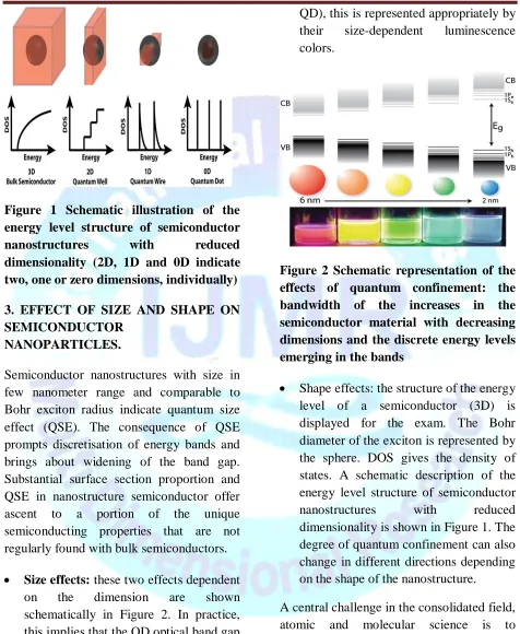
Figure 1 Schematic illustration of the energy level structure of semiconductor
nanostructures with reduced
dimensionality (2D, 1D and 0D indicate two, one or zero dimensions, individually)
3. EFFECT OF SIZE AND SHAPE ON SEMICONDUCTOR
NANOPARTICLES.
Semiconductor nanostructures with size in few nanometer range and comparable to Bohr exciton radius indicate quantum size effect (QSE). The consequence of QSE prompts discretisation of energy bands and brings about widening of the band gap. Substantial surface section proportion and QSE in nanostructure semiconductor offer ascent to a portion of the unique semiconducting properties that are not regularly found with bulk semiconductors.
Size effects: these two effects dependent
on the dimension are shown
schematically in Figure 2. In practice, this implies that the QD optical band gap
can be adjusted substantially by
changing its size. For QDs emitted on the obvious (for example, CdTe or CdSe
QD), this is represented appropriately by
their size-dependent luminescence
colors.
Figure 2 Schematic representation of the effects of quantum confinement: the bandwidth of the increases in the semiconductor material with decreasing dimensions and the discrete energy levels emerging in the bands
Shape effects: the structure of the energy level of a semiconductor (3D) is displayed for the exam. The Bohr diameter of the exciton is represented by the sphere. DOS gives the density of states. A schematic description of the energy level structure of semiconductor
nanostructures with reduced
dimensionality is shown in Figure 1. The degree of quantum confinement can also change in different directions depending on the shape of the nanostructure.
matter involves particles of ~ 1023 cm-3
that cooperate through the limitless
limitation of Coulomb, which is responsible for the exciton plan (series of electron holes
connected) and persistent associations
between them.
The coupling of solid solid matter is also possible by the incrustation of a QW in a semiconductor microcavity, which causes states of hybridized excitons-polaritons; The 2D quantum spectra of two, three and four are particularly delicate for the cooperation between the different branches of the polaritons. Because the QW dimensionality is reduced to a nuclear thickness, for example, in single-layer van der Waals
semiconductors, improved dielectric
screening improves Coulomb cooperations
and electron connections. In 2D
spectroscopy, solid impacts many bodies appear as pinnacles confined excitons identified impartial biexcitones loaded
excitons and combined with greater
demands for estimating restrictive vitality in contrast to semiconductors higher level dimensionality. The exciton-exciton-phonate connections cause a rapid displacement at high exciton density and the exciton-phonon dispersion improves vitality movement in the 2D monolayers and, in addition, in 1D carbon nanotubes. Exchange vitality and goods further accept a fundamental part of photovoltaics, in which the age of multiple excitons in PBS photocells produces
unequivocally highlighted photocurrent
dispersive 2D spectroscopy that are difficult to distinguish between different strategies.
4 NANOPARTICLES SYNTHESIS
METHODS
Wet Chemical Methods
The term "organic-hybrid inorganic" materials emerged recently with the process of the birth of "soft" inorganic chemistry, particularly solvotérmico / hydrothermal and sol-gel process, which is probably the process of soft supreme inorganic chemistry, allowing an adapted chemical design. The
unique low-temperature processing
characteristics of this process allows the chemical design of organic-inorganic hybrid materials through the incorporation of low-molecular-weight organic molecules with appropriate inorganic functional portions at temperatures that do not destroy organic.
5. BEHAVIOR OF
SEMICONDUCTORS IN ELECTRIC
FIELD IN BULK AND
NANOSTRUCTURES
The physical properties of a semiconductor are found to be affected by the application of an external electric field. The formation of two-dimensional electron-gas layer (Q2D system) is one such example in MOS devices and this is the result of the band-bending when an external electric field is applied. A semiconductor structure of still lower dimensions may be achieved by applying an electric field in the plane of the Q2D system where the applied field squeezes the dimension from Q2D to Q1D. Similarly, a QOD structure may be realized by applying suitable electric field across a Q1D system.
of any field, the threshold frequency (m) for band-edge absorption is (Egfh), where Eg
being the band-gap energy. With an externally applied electric field, a shift is observed in the red absorption limit towards the longer wavelengths and the amount of shift may be of the order of few hundred angstroms for reasonably high field. This is very well-known „Franz-Keldysh effect1 in bulk semiconductor. The Franz-Keldysh
effect is the result of
wavefunctions"leaking" into the band gap.
Another interesting effect is observed with high electric field (the field strength is of the order of 109V/m) where electrons may come out of the semiconductor. This is due to the fact that the potential barrier gradually decreases with the distance from the semiconductor surface when such high field is applied. Thus, the electrons will have the possibility of tunneling through the barrier and escape from the semiconductor. This phenomenon is known as field emission or cold emission of electrons. As the submicron structures of semiconductor have discrete energy states, the current density of such emitted electrons will be modified by the dimensions of the structure. This gives rise to many interesting and unusual features of field emission. Thus, all such effects that depend largely on the band structure may also be controlled in an interesting way with the application of external electric field on a low-dimensional structure.
6.BEHAVIOR OF SEMICONDUCTORS IN A MAGNETIC FIELD IN BULK AND NANOSTRUCTURES
Landau quantization of electron states is an important and well-known effect of the application of an external magnetic field on a semiconductor. Due to this quantization, the motion of the electrons become restricted in the plane perpendicular to the magnetic field and electrons can only move in some quantum mechanically allowed orbits in that plane. The free motion of electrons is possible only along the direction of the magnetic field
7. ADVANTAGE OF
SEMICONDUCTOR NANOMATERIALS
Semiconductor nanomaterials have
interesting physical and chemical properties and useful functionalities, compared to
conventional mass counterparts and
molecular materials. The most interesting features of these materials are close-spectrum spectra and emission bands with
intensive continuous absorption, high
chemical stability and photobleaching, processing capacity and surface operation. The development of "Nanochemistry" is reflected in a large number of publications
on the synthesis of semiconductor
nanoparticles Alexander, (2005)[2]. For example, the effect of spatial quantum confinement produces a significant change in the optical properties of semiconductor nanomaterials. The very high dispersion (high surface-to-volume ratio), with physical
and chemical properties of the
and have aroused great interest in research and applications in various fields, such as solid-state physics, inorganic chemistry,
physical chemistry, colloid chemistry,
science of materials and biology recently. Sciences, medical sciences, engineering and interdisciplinary fields. Among the unique properties of nanomaterials, the movement of electrons and gaps in nanomaterial semiconductors is determined essentially by the quantum confinement and known
containment properties are connected
phonons and photons are influenced largely by the size and geometry of the materials (Alivisatos, 1996[3], Alivisatos 1996[4], Burda et al 2005[5], Murray et al 2000[6]). The specific surface area and surface area increases the volume ratio considerably as the material size decreases (Alivisatos 1996[3], Chen, et al. 2005[7]).
8. CONCLUSION
Behaviour of semiconductor nanostructures
also changes significantly with the
application of electric and magnetic field. Thus, the studies on electron states are important because it can explain the physical properties of novel semiconductor structures discussed in this chapter. Photoemission from a degenerate n-type semiconductor has been studied helps to understand the band structure and electron states of the conduction band of a semiconductor which is discussed in next chapter. It appears, therefore, that the investigations on the physics of degenerate semiconductors with nanoscopic dimensions are quite- promising area of active field research.
Semiconductor nanomaterials are advanced materials for various applications, which have been discussed in detail. The unique physical and chemical properties of the semiconductor nanomaterial make it suitable for application in emerging technologies such as nanoelectronics, nanophotonics,
energy conversion, nonlinear optics,
miniaturized sensors and imaging devices, solar cells, detectors, photography and biomedicine. There are three key steps in the
development of nanoscience and
nanotechnology: preparation of materials, characterization of properties and device
production. The preparation of
nanomaterials has been advanced by numerous physical and chemical techniques. The purification techniques and the selection of the developed dimensions can produce nanocrystals with a well-defined structure and morphology.
We have discussed so far, the effects of electric field and magnetic field on semiconductor nanostructures separately. But, it has been observed that the results will be more interesting if both electric and magnetic fields are applied simultaneously,
particularly, in the crossed-field
configuration. The analysis of a quasi-low-dimensional semiconductor structure in crossed electric and magnetic field is very much useful in determining the effective masses of electrons and holes in conduction and valence band respectively. Strictly speaking, the quantum Hall effect mentioned earlier is the direct consequence of crossed fields. Various research works have already
been reported in the crossed field
that F/B ratio (F being the electric field and
B, die magnetic field intensity) plays an
important role on the behavior of
semiconductor nanostructures. In a
subsequent chapter investigation will be carried out for a particular submicron structure placed in the crossed fields.
The fundamental research areas covered by Research the Centre include semiconductor physics, nanostructure physics, scanning probe methods, surface and interface physics, magnetism and low temperature physics, as well as solid state theory. A close collaboration among the research groups of the Centre exists for the fabrication as well as characterization of artificially micro- and
nanostructured materials, including
semiconductors, metals, superconductors and magnetic systems. Furthermore, the strong interaction between experiment, theory and computer simulation plays an
important role for advances in the
understanding of fundamental properties of micrometer- and nanometer-scale structured materials.
In order to gain a deeper insight into the
(photo)carrier behavior by SPCM
measurements, further efforts should be directed towards the fabrication of Ohmic CdS nanowire devices. Here, Group III metals such as gallium and indium might offer an interesting alternative, since the successful doping with indium has already been demonstrated. Further investigations on the dopant distribution within indium and manganese doped CdS wires could be performed by SPCM and tomographic methods. Owing to their highly anisotropic shape and their availability in great quantities, CdS nanowires might be used for the fabrication of polarization sensitive photodetectors. Furthermore, the integration of CdS wires into novel organic–inorganic hybrid solar cells or their use for photocatalysis offers intriguing prospects for future applications
REFERENCES
[1]. R. P. Feynman. There‟s plenty of room at the bottom. Caltech‟s Engineering and Science Magazine, February 1960.
[2]. Alexander, E. Angew. Chem.Int. Ed. 2005, 44, 4839.
[3]. Alivisatos, A. P. J. Phys. Chem. 1996, 100, 13226.
[4]. Alivisatos, A. P. Science 1996, 271, 933.
[5]. Burda, C.; Chen, X.; Narayanan, R.; El-Sayed, M. A. Chem. Rev. 2005, 105, 1025.
[6]. Murray, C. B.; Kagan, C. R.;
Bawendi, M. G. Annu. Rev. Mater. Sci. 2000, 30, 545.