ISSN (Print) : 2320 – 3765 ISSN (Online): 2278 – 8875
I
nternational
J
ournal of
A
dvanced
R
esearch in
E
lectrical,
E
lectronics and
I
nstrumentation
E
ngineering
(An UGC Approved Journal)
Website: www.ijareeie.com
Vol. 6, Issue 8, August 2017
Design and Development of Universal Switch
Mode Power Supply
Jagdish1, Dr. R.Jayapal2
PG Student [Power Electronics], Dept. of EEE, R.V College of Engineering, Bengaluru, Karnataka, India1
HOD & Professor, Dept of EEE, R.V College of Engineering, Bengaluru, Karnataka,India2
ABSTRACT: This paper presents the design and development of an universal switch mode power supply that is operated with either an AC or DC input supply. The fly-back topology is chosen for developing the universal SMPS because it is suitable for low power off-line switching converters and also simpler and versatile. The fly-back converter is operated in continuous conduction mode (CCM). In this project TOP258PG controller integrated chip is used. The main feature of this controller is that it has inbuilt MOSFET. Therefore, the number of components reduces. This leads to the compact size and reduced weight of the converter. The proposed converter delivers output voltage of 12V/2A DC.The converter is operated with fixed switching frequency of 66 kHz.
KEYWORDS:Fly-back Converter Continuous conduction mode, Universal SMPS, Window Utilization Factor.
I.INTRODUCTION
Power supplies are used widely for most of the real time applications. They are categorized as linear and switched mode power supplies [1]. In the linear power supply switch is operated in linear region of switch, so in linear region losses are high [2][3]. The SMPS having electronic switch that operates in saturation and cut-off region. Hence the losses are reduced and efficiency is high [4][5]. SMPS are categorized into two types –Isolated and non-isolated topologies. The main difference between the two is that, in isolated power supply, the output power stage is isolated from input by means of isolating transformer or isolators. In non-isolated power supply, the switching transients are injected from load to the input and control circuit. Isolated topologies enable the converter to operate at different reference potentials. SMPS are efficient, highly reliable and can bear varying environmental conditions. This noticeable feature coupled with the advent of modern power electronic converters has enabled the use of SMPS in fields of Telecom, Military and Aerospace domains [6].
This paper proposes the use of current mode controlled single output flyback converter. The shunt regulator is used at the output to achieve better line and regulation of the output 12V/2A is achieved by using LM431 shunt regulator IC [7]. The protection circuit such as overecurrent protections(OCP) and Short Circuitsprotection (SCP),Over VoltageeProtection (OVP) and Under VoltageeProtection (UVP) Circuits have also been provided by the controller IC TOP258PG [8].
ISSN (Print) : 2320 – 3765 ISSN (Online): 2278 – 8875
I
nternational
J
ournal of
A
dvanced
R
esearch in
E
lectrical,
E
lectronics and
I
nstrumentation
E
ngineering
(An UGC Approved Journal)
Website: www.ijareeie.com
Vol. 6, Issue 8, August 2017
II.OPERATION AND DESIGN PROCEDURE
A.Block Diagram
The block-diagram of the proposed system is as shown in the Fig.1. This consists of following block.
Fig.1.Block diagram representation
The AC input supply voltage varying in the range of 85-265V with frequency 50Hz or DC input supply is applied to the input filter and nominal voltage is 240V.
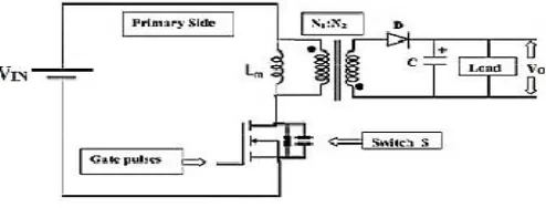
B. Working principle
The operation is similar to the typical flyback topology as shown in the Fig.2. It consists the fast switching device (MOSFET), fly-back transformer. The primary winding of this transformer is connected in series with the switch and secondary winding connected to the output filter and load. Practically, due to the presence of finite magnetization and leakage inductance, the losses occur in the transformer. The losses also occur in the switch and the output diode, these losses tend to reduce the overall efficiency of the converter. The use of clamper circuit across the MOSFET switch is significantly improves the performance of the converter[1][2].
Fig 2.Basic fly-back converter topology
ISSN (Print) : 2320 – 3765 ISSN (Online): 2278 – 8875
I
nternational
J
ournal of
A
dvanced
R
esearch in
E
lectrical,
E
lectronics and
I
nstrumentation
E
ngineering
(An UGC Approved Journal)
Website: www.ijareeie.com
Vol. 6, Issue 8, August 2017
this takes place before the control pin voltage can discharge to the threshold voltage of lower value of around 4.8V. Once, the control pin charges to the voltage value of a shunt regulator of 5.8V due to externally feeding current, the current in excess of the consumption of a chip is shunted to source by the NMOS current mirror. The duty cycle of the power MOSFET is controlled by the output current of the NMOS current mirror to provide the closed loop regulation [8]. Thus by this closed loop regulation, a constant voltage is obtained at the output.
C. Converter Specification
Input Voltage: 85V to 265V AC or 75V to 375V DC
Switching frequency: 66kHZ
Power output: 24W
Output voltage and current: 12V/2A DC
Efficiency: ≥80%
Lineeand loaderegulation: ≤1%
Rippleeand Noise: ≤1% of output voltage
D. Design Procedure
The work presented includes the design of fly back transformer, input filters. The selection of rectifying diodes and output capacitors also play an important part in the converter design. Design of fly back transformer, selection of Controller IC and selection of output diode are explained in the following sections D1, D2, D3 [7]-[8].
D1.Flyback transformer design
In this proposed work, ferrite core is selected .The area product (AP) is obtained by equation (1) [10]-[12].
=
( ( ))
∗ ∗ ∗ (1)
Where
Kw = windowutilizationfactor = 0.4 J = currentdensity = 4 A/mm2
Bm= ΔB= flux density of the core= 0.2 Tesla
fsw = switching frequency
The maximum duty cycle is 65%.The primary and secondary rms current is given by equation (2),(3) and the turns ratio(Tratio) is obtained by equation (4)
IPRMS =Ip * Dmax K2p
ISSN (Print) : 2320 – 3765 ISSN (Online): 2278 – 8875
I
nternational
J
ournal of
A
dvanced
R
esearch in
E
lectrical,
E
lectronics and
I
nstrumentation
E
ngineering
(An UGC Approved Journal)
Website: www.ijareeie.com
Vol. 6, Issue 8, August 2017
Fig.3. Schematic diagram of Proposed Converter
ISRMS = Isp* 1-Dmax Kp2
3 −Kp+1 (3)
Tratio=
Np NS=
VOR
(V0+VD) (4)
Depending on the area product, selected core is EF25 which has the following specifications [11][12][13],Area Product (Ap) 3202 mm4, Cross sectional area (Ac) 52.50 mm2, Window area (Aw) 61.00 mm2, Core volume (Ve) 3020 mm3,
Core gap: 0.55mm.
D2.Selection of Controller IC
The controller IC is selected based on current, voltage and temperature ratings required for the particular application. The functional block diagram of a controller IC is as shown in the Fig.4. In this proposed work, TOP258PG controller IC is used.TOP258PG is an integrated SMPS chip [8].
Fig.4.Functional block diagram of controller IC D3.Selection of output diode
ISSN (Print) : 2320 – 3765 ISSN (Online): 2278 – 8875
I
nternational
J
ournal of
A
dvanced
R
esearch in
E
lectrical,
E
lectronics and
I
nstrumentation
E
ngineering
(An UGC Approved Journal)
Website: www.ijareeie.com
Vol. 6, Issue 8, August 2017
Power loss in output diode is
PD=Vf *Iout (5)
PD=0.95*2=1.9W= 0.95 * 2=1.9W
III. Experimental setup and Results
A. Experimental setup
The input supply voltage is varied from 85V-265V AC/DC. The experimental setup for the proposed work is as shown in the Fig.5 (a),(b) for both AC and DC input voltage, and the output voltage maintained constant at 12V/2A.
Fig.5 (a) Test setup of the proposed converter with AC input voltage, (b) DC input Voltage
B. Experimental Results
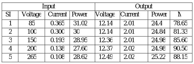
B1.Efficiency results
The converter is operated at 66 kHZ from 85V to 265V input range and the output voltage is measured. Table 1 tabulates the efficiency at different input voltage at full load.
TABLE 1.EFFICENCY AT FULL LOAD
Input Output
SI Voltage Current Power Voltage Current Power η
1 85 0.365 31.02 12.14 2.01 24.4 78.65 2 100 0.300 30 12.14 2.01 24.84 81.33 3 150 0.193 28.95 12.36 2.01 24.98 85.60 4 200 0.138 27.60 12.37 2.02 24.98 90.50 5 265 0.108 28.62 12.49 2.02 25.22 88.15
The efficiency of converter tabulated in the TABLE 1 at full load matches with the required specification.
B2. Line and Load Regulation
The line and load regulation are calculated using the Eq.6 and Eq.7 and both should be within the specification limit of
± 1% as tabulated in the Table 2 for AC input and Table 3 for DC input.
%Load Regulation=VMin_Load VMax_Load
VNom_Load ∗100 (6)
%Line Regulation=VIn_Min VIn_Max
ISSN (Print) : 2320 – 3765 ISSN (Online): 2278 – 8875
I
nternational
J
ournal of
A
dvanced
R
esearch in
E
lectrical,
E
lectronics and
I
nstrumentation
E
ngineering
(An UGC Approved Journal)
Website: www.ijareeie.com
Vol. 6, Issue 8, August 2017
TABLE2.LINEANDLOADREGULATIONATDIFFERENTLOAD
FORACINPUT SI Input
Voltage
Output Voltage half load(50%)
Output Voltage Full load (100%)
Load Regulation (%) 1 85 12.37 12.35 0.161 2 100 12.38 12.34 0.323 3 150 12.57 12.57 0 4 200 12.58 12.57 0.079 5 265 12.49 12.47 0.1602 Line
regulation
-0.96 -0.96
-
TABLE 3. LINE AND LOAD REGULATION AT DIFFERENT LOAD FOR DC INPUT
SI Input Voltage
Output Voltage half load (50%)
Output Voltage Full load (100%)
Load Regulation (%) 1 85 12.37 12.37 0.0 2 100 12.25 12.23 0.163 3 150 12.37 12.37 0 4 200 12.40 12.37 0.242 5 265 12.49 12.47 0.160 Line
regulation
-0.965 -0.805 -
The load and line regulations tabulated in TABLE 2 and TABLE 3 for different input voltage supply ranging from 85V to 265V and from the this results, it is noticed that the load and line regulation are within the specification limit of ±1%.
C. Observed Waveforms
In this sectionoutput voltage waveforms captured are presented as follows:
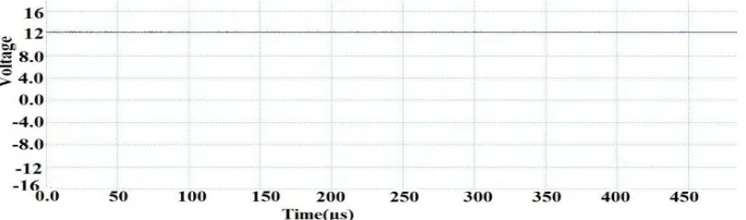
C1. Output voltage wave forms
The output voltage waveform are observed at different input AC or DC supply voltages and is found to be 12V at full load of 2A.The output voltage of 12V at minimum input supply voltage being AC or DC of 85V is as shown in the Fig.6 (a) and it is same as the required specification.
Fig.6 (a) Output voltage waveform at minimum input voltage
ISSN (Print) : 2320 – 3765 ISSN (Online): 2278 – 8875
I
nternational
J
ournal of
A
dvanced
R
esearch in
E
lectrical,
E
lectronics and
I
nstrumentation
E
ngineering
(An UGC Approved Journal)
Website: www.ijareeie.com
Vol. 6, Issue 8, August 2017
Fig.6 (b).Output voltage waveform at maximum input voltage
IV. CONCLUSION
The current mode controlled fly-back converter with fixed frequency having output voltage and current 12V/2A DC is designed and developed. Results are verified with the prototypeehardwareemodellhaving an output 12/2A. Protection is provided internally by a controller IC TOP258PG.Converter module is designed to meet up the power supply requirement for relay operation.
REFERENCES
[1] A.I. Pressman, “Switching Power Supply Design”, McGraw Hill, 1991.73. [2] Daniel Hart, “Power Electronics”, McGraw Hill,2011
[3] Qiang Wu, Zhangming Zhu “An Adaptive High-precision OCP Control Scheme for Flyback AC/DC Converters”,IEEEITrans.Power Electron.,vol.32,no.2, pp. 8969 – 8973,04 May 2017.
[4] Qiang Wu, Zhangming Zhu “A Versatile OCP Control Scheme for Discontinuous Conduction Mode
FlybackiAC/DCIconverters”,IEEETrans.Ind.Electron.,vol.64,pp.6443-6452,14 March 2017.
[5] B.V Adarsh, LathaShenoy “Flyback topology based Power Amplifier for PV system Applications” 2016 International Conference on Computation of Power, Energy Information and Communications(ICCPEIC) ,Chennai, Tamil Nadu, India, 01 September 2016.
[6] Kanthimathi, R., and J. Kamala. "Analysis of different flyback Converter topologies", 2015International Conference on Industrial Instrumentation and Control (ICIC), Chennai, Tamilnadu, India, pp 1248 – 1252, 28-30 May 2015.
[7] Application note TOP258PG from Power integration. [8] Data sheet TOP258PG, PC817A, LM431.
[9] AlenkaHren, Member, JozeKorelic, and MiroMilanovic, “RC-RCD Clamp Circuit for Ringing Losses Reduction in a Flyback Converter”, IEEE Transactions on Circuits and Systems—II: Express Briefs, vol. 53, no. 5, pp. 369-373, May 2006.
[10] T. Kitagawa and T. Mitsui, “Ferrite core for switching regulator”, IEEE Translation Journal on Magnetics in Japan, vol. TJMJ-1, no. 6, pp. 665-663, Sep 1985.
[11] Umanand L. and Bhatt S R, “Design of Magnetic Components for Switched Mode Power Converters”, Wiley Eastern Publication, 2009. [12] NasrudinAbd. Rahim and Ahmad Maliki Omar, “Ferrite Core Analysis for DC-DC Flyback Converter”, TENCON, Kuala Lumpur, vol. 3, pp.
290-294, 24-27 Sep 2000.
[13] Zhang. X, Liu. H, and Xu. D, “Analysis and design of the flyback transformer”, 29th Annual Conference IEEE on Industrial Electronics Society ( IECON), vol. 1, pp. 715-719, 2-6 Nov. 2003.
[14] Jiaxin Chen, Jianguo Zhu, and YouguangGuo “Calculation of Power Loss in Output Diode of a Flyback Switching DC-DC Converter”, 5th CES/IEEE International Power Electronics and Motion Control Conference (IPEMC), Shanghai, vol. 6, pp. 1-5, 14-16 Aug 2006.