Volume 2006, Article ID 12945, Pages1–16 DOI 10.1155/WCN/2006/12945
Parametric Conversion Using Custom MOS Varactors
Howard Chan,1Zhongbo Chen,1Sebastian Magierowski,1and Krzysztof (Kris) Iniewski2 1Department of Electrical and Computer Engineering, University of Calgary, Calgary, AB, Canada T2N 1N4 2Department of Electrical and Computer Engineering, University of Alberta, Edmonton, AB, Canada T6G 2V4
Received 14 October 2005; Revised 17 April 2006; Accepted 18 April 2006
The possible role of customized MOS varactors in amplification, mixing, and frequency control of future millimeter wave CMOS RFICs is outlined. First, the parametric conversion concept is revisited and discussed in terms of modern RF communications systems. Second, the modeling, design, and optimization of MOS varactors are reconsidered in the context of their central role in parametric circuits. Third, a balanced varactor structure is proposed for robust oscillator frequency control in the presence of large extrinsic noise expected in tightly integrated wireless communicators. Main points include the proposal of a subharmonic pumping scheme based on the MOS varactor, a nonequilibrium elastance-voltage model, optimal varactor layout suggestions, custom 0.13μm-CMOS varactor design and measurement, device-level balanced varactor simulations, and parametric circuit evaluation based on measured device characteristics.
Copyright © 2006 Howard Chan et al. This is an open access article distributed under the Creative Commons Attribution License, which permits unrestricted use, distribution, and reproduction in any medium, provided the original work is properly cited.
1. INTRODUCTION
Variable capacitors can play a very rich role in radio-fre-quency (RF) transceivers. In this paper we examine their use in two key front-end functions: amplification and frequency control. Parametric amplification, a relatively uncommon technique, is promoted in this paper. Improvements to this method are proposed by the incorporation of customized MOS varactors in place of the traditional junction varactor. Also, we discuss modifications to the MOS varactor in the context of its traditional role as a frequency control element. Anticipating a growing problem with interference between IC elements sharing one substrate, a four-terminal diff eren-tial structure intended to desensitize voltage-controlled oscil-lators (VCOs) to large extrinsic noise variations is described. The paper is organized as follows. First a narrow out-line of the history and status of parametric amplification is given inSection 2. A more detailed discussion of paramet-ric circuit operation, improvements, and possible incorpo-ration in a front-end transceiver is discussed in Section 3. Since the varactor constitutes the heart of parametric sys-tems, Section 4 outlines the key integrated varactor struc-tures, compares them based on two key merit figures, and in-troduces potential device-level augmentations. InSection 5 we return to parametric circuits and, with the results of Section 4, estimate the performance possibilities for an inte-grated setting. Frequency control, the second key topic of this report, is discussed inSection 6. This is approached from the
device level, where the advantage and limitations of employ-ing a modified common-mode rejection varactor structure in a voltage-controlled oscillator (VCO) are discussed.
2. PARAMETRIC CONVERSION: HISTORICAL REMARKS
Parametric circuits closely tie frequency conversion to am-plification and therefore can seamlessly account for the mix-ing function of front ends as well. We broadly refer to them as parametric converters in this work. They are primarily known for their low-noise behavior and ability to operate at high frequencies.
As implied by its name, parametric conversion involves the modulation of a system’s parameters as in the damped oscillatory equation below:
¨
x+γx˙+ω2 0
1 +p(t)x=0. (1)
Given a pumping disturbance at twice the oscillator’s natural frequency,
p(t)=Apsin
2ω0t
, (2)
Asubharmonic (relative to the pump) response
can be solicited whereαranges between positive and neg-ative values depending on the oscillator damping and the strength of the pumping signal. It is commonly acknowl-edged that such sustained parametric oscillations were first observed by Michael Faraday. In 1831 he reported the rise of subharmonic oscillation as part of experiments on acousti-cally pumped Chladni plates [1]. In 1957, following sugges-tions by Suhl [2] and Weiss [3], he reported the realization of an experimental solid-state microwave amplifier exploit-ing the parametric principle. Notable among a large num-ber of intermediate contributions is Hartley’s work on elec-tromechanical parametric amplifiers [4,5] and Barrow’s fully active parametric vacuum tube implementation [6]. This space has been a subject of interest in the MEMS arena for low-frequency, precision sensing applications such as atomic force microscopy [7,8] where the low-noise properties of parametric systems are of particular benefit. However, the use of parametric amplification in terrestrial communication systems is extremely rare. Recently, a discrete time paramet-ric circuit in a 0.25μm-CMOS technology was reported [9]. The circuit took particular advantage of the three-terminal inversion mode MOS varactor, but focused on low-frequency applications in the 100 kHz range.
The absence of parametric converters from the commu-nications mainstream is mainly due to the superior utility of transistor-based circuits for “low-” frequency commercial applications. Since the performance of parametric circuits is less dependent on the lateral dimensions (and hence de-lay) of their components, a key advantage of this approach is its ability to operate at higher frequencies early in the nology life cycle. However, improvements in transistor tech-nology steadily encroached on the high-frequency reserve of parametric circuits thus marginalizing this advantage. Since more remote regions of the spectrum were better accommo-dated by maser and laser amplifiers, a loss of interest in the parametric circuit approach followed.
Today, as personal commercial communications applica-tions migrate to more exotic frequency domains, a niche for the parametric circuit may resurface. This may especially be the case for low-profile millimeter wave electronics intended for dense sensor or distributed network applications. Size and power constraints exclude many of today’s molecular amplifiers (although integration progress has been substan-tial [10]) from consideration while performance, power, and approaching physical limits have relegated millimeter wave applications to the domain of expensive IC technologies.
3. PARAMETRIC CONVERSION: TECHNICAL REMARKS
Conventional electronic transistor amplifiers operate by us-ing a small signal to modulate the resistance of a switch that, in turn, mediates the coupling between a large DC supply and a load. Amplification is achieved because the coupling is proportional to the small input signal and is efficient be-cause, ideally, the supply does not influence the modulated resistance. Alternatively, parametric amplifiers utilize a non-linear reactance (in this paper we consider only capacitive re-actances) through which an AC supply “energizes” a small
signal. More specifically, a small signal deposits charge on a capacitor. An AC “pump” increases the potential energy of this charge by increasing the capacitance, the pumped charge is then siphoned offto a load.
Immediately it is apparent that by foregoing resistive cou-pling such an amplification principle sidesteps, at least in part, thermal fluctuations and holds inherent noise behavior advantages. A handy “existance theorem” of sorts for para-metric converters is available in the form of the Manley-Rowe relations [11]
The ideal circuit used to derive the Manley-Rowe relations is shown inFigure 1. These relations constrain the power,Pm,n, absorbed by a nonlinear capacitor at frequenciesm fs+n fp that is driven by two sources operating at frequencies fs(the signal source) and fp (the pump source). The relations are fundamental in that they are based on the principle of en-ergy conservation (zero total average power flowing into the capacitor) and are independent of the capacitance-voltage (CV) characteristics (aside from assuming no hysteresis in the voltage); the relations are limited in that they do not ac-count for losses in the varactor which have a substantial im-pact on practical implementations.
The raw circuit performance encapsulated by Manley-Rowe relations needs to be constrained in order to realize practical functions like upconversion (signal at fsamplified and mixed to higher frequencies) or downconversion (sig-nal atfsamplified and mixed to lower frequencies) or simply straight amplifiers (signal atfsamplified atfs). The common way of doing this is to encase the capacitance in a multimode cavity. From a lumped circuit perspective, this means con-necting the capacitance to some assembly of resonators.
3.1. Upper-sideband upconverter
We imagine the nonlinear capacitor locked in a resonant con-figuration that allows power to flow only at frequencies fs,fp, and fu= fs+fp. For this scenario equation (4) is simplified
Es
+ +
Ep
fs fp fs+fp fs fp fs+ 2fp m fs+n fp
Figure1: The ideal parametric converter used to derive the Manley-Rowe relations. Ideal impedance filters allow only a single tone to flow through any one branch.
to a load. From (5) the circuit has the operating power gain
Gup=Pu
Ps =
fu
fs.
(7)
A more physical description of USBUC operation may shed more light on its behavior. The potential energy of the charge that a small signal deposits on a capacitor can be in-creased by separating that charge. Work is needed to do this and this work is periodically supplied from a pump circuit. Under this condition, when a load extracts this charge from the capacitor, it will have access to higher energy carriers. Gain is achieved. However, the work used to energize the mediating capacitor increases the energy needed by the in-put signal to charge it again. Thus, the circuit is naturally at an advantage when pumping and energy extraction are done quickly compared to the dynamics of the signal input (i.e., when the capacitor signal is oversampled).
Thus the higher the output frequency (hence pump), the greater the circuit gain. This configuration, the upper-sideband upconverter (USBUC), is well suited for high-frequency transmission. For instance, under ideal conditions, converting a 6 MHz signal to a 60 GHz carrier promises a 40 dB operating power gain making the circuit more attrac-tive for millimeter wave applications. Note that, under the ideal described by (5) and (6) (i.e., lossless varactor and perfect resonator), the gain is completely independent of the pumping power. Analysis and simulations of the impact wrought by varactor losses on circuit gain are presented in Section 5. Of course the maximum available output power is limited by the size of the input and pump signals. For a small input signal and fu fswe have a maximum output power of approximatelyPp/2 hence an efficiency of 50%. As fs in-creases the efficiency improves, but the gain drops.
Accounting for losses in the surrounding filter (cavity) network by itself does not directly influence the ideal gain prediction. Rather, as highlighted by Rowe [12], the band-width of the converter is compromised. Assuming that the pump’s action on the nonlinear varactor introduces a time-varying incremental capacitance between the USBUC’s fs and fuports of
Cpump(t)= ∞
n=−∞
Cnej2πn fpt (8)
the bandwidth to signal-frequency ratio (γup/ fs) becomes [12]
γup
fs =
C1
C0
2fu
fs.
(9)
Returning to the previous example, to accommodate a signal of 10 MHz bandwidth converted from a 6 MHz to a 60 GHz center frequency requires aC1/C0ratio of less than 1/80. This bodes extremely well for the pump. For a well-designed MOS varactor it is not unreasonable to expect a 50% variation aroundC0, that is, assuming the common empirical MOS model we expect
CMOS=C0+C0 2 tanh
3 2vpump
≈C0+3C0
4 vpump, (10)
where the latter approximation is based on the assumption of a small pump voltage. This is confirmed by the smallC1/C0 requirements of our example. From (9) and (10), a peak-to-peak pump voltage of only 16 mV is needed to sufficiently perturb the varactor so that a 10 MHz bandwidth is estab-lished. This must be tempered with the fact that in this case the pump needs to operate at 60 GHz which is not out of the question for production level technologies (albeit a sig-nificant stretch for CMOS) exploiting distributed operation [13], frequency doubling [14], or second-harmonic gener-ation [15]. Further, it is possible to redesign the pumping scheme of the parametric converter to continue meeting the Manley-Rowe predictions while operating with a pump at lower frequencies. This is discussed inSection 3.3.
The benefits available to the USBUC become serious im-pairments when considering this topology for a receiver’s downconversion block. The substantial gain available to the upconverter (7) becomes a tremendous loss as, naturally,
fu fsfor downconverters. Fortunately, a large variety in parametric conversion topologies exists, some of which do allow for gain in the downconversion arrangement. One such topology is discussed presently.
3.2. Lower-sideband downconverter
case, the converter’s cavity is aligned such that power only at fs (the RF signal), fp, and fd = fp − fs (the down-converter signal) can flow through the circuit. To obtain a low-frequency output, the constraints fp > fs (otherwise an upper-sideband downconverter is realized) and fp <2fs (otherwise a lower-sideband upconverter (LSBUC) is real-ized) must hold. Returning to the Manley-Rowe relations we get
which, given that the pump power flows into the circuit, im-plies that power emerges from the converter’s input (signal) port despite an input signal being fed into the receiver (e.g., from an antenna). Hence, the impedance of the LSBDC’s sig-nal port is negative. Similarly, (12) states that the pump en-ergy causes power to emerge from the downconversion port as well. Being related to the power emerging from the sig-nal port (see (11)) this implies that the downconversion port impedance is also negative. The LSBDC doubles as a reflec-tion amplifier.
The operation of this circuit can be summarized as fol-lows. The pump generates the highest frequency “signal” in the circuit. Thus, unlike the USBUC, on average it can couple power from the signal port (RF) to the downconversion port (IF) and vice versa. As with the USBUC, the power coupling and amplification is mitigated by work done by the pump in changing the varactor capacitance. Since the pump switches only slightly faster than the signal, it transfers a relatively small amount of the input power into the downconversion port’s IF frequency. However, being much higher than IF, the pump taps, amplifies, and converts a great deal of the IF back to RF (as predicted by (11)). Part of the larger input signal is then tapped once again by the pump and fed into the down-conversion port. A positive feedback is established and the circuit functions as a regenerative amplifier. Thus the pump power emerges as RF and IF frequencies from the respec-tive ports which now have a negarespec-tive input resistance. The more power that is pumped into the circuit is, the higher the quality factor,Q, of the RF and IF modes is. Thinking of the input as a forcing signal on these modes we can automati-cally see that the higher theQ, the higher the signal gain, but the lower the bandwidth. Nonetheless, for signals centered around millimeterwave carriers, the LSBDC topology has a lot of relative bandwidth performance to sacrifice. What is a drawback to this circuit, however, is that an excess of pump power leads to instabilities (overcompensation of loss) and, simultaneously, a greater sensitivity to component variations (thus increasing the likelihood of instability). However, the advantage remains the potentially low-noise behavior about which the Manley-Rowe relations say nothing. We return to this inSection 5.
Figure2: A simple transmit chain employing the USBUC.
3.3. Parametric transmit and receive chains
How can parametric converters be assembled into the transceiver chain? Since they combine oscillator, mixer, and amplifier functions under essentially one circuit, they hold the potential to form the basis for a diverse set of radio sys-tems.
Perhaps the most straightforward application is the use of an USBUC as a low-voltage upconverter of BB or IF signals to millimeter RF. For minimal complexity and power consump-tion, the design inFigure 2can be used. This diagram sug-gests interfacing the USBUC directly to the antenna which, if the antenna is sufficiently narrowband, can serve as the upper-sideband bandpass filter. Employing a standard two-terminal varactor structure in this topology will impose ex-tra gain limiting—significant upconverted signal amplitudes can induce lower-sideband signals to flow (i.e.,ωp−ωs) thus returning power back to the input source. A simple alterna-tive is to use the USBUC as an upconverting mixer and pre-amplifier and leave the final millimeter wave amplification to a dedicated high-frequency (and high-cost) power amplifier. Alternatively, a double-balanced varactor structure (as de-scribed inSection 4.3in the context of VCO frequency con-trol) can be used in an attempt to desensitize the varactor ca-pacitance to variations in the upconverted signal frequency.
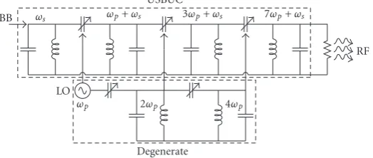
BB ωs
USBUC
ωp+ωs 3ωp+ωs 7ωp+ωs
RF
LO
ωp 2ωp 4ωp
Degenerate
Figure3: Multistage USBUC transmitter with degenerate pump.
RF ωs
LSBDC ωd
IF
ωs
ωp
ADC
ADC
Figure4: Receive chain using a LSBDC as a mixer and amplifier.
re-radiation and help maintain stability. A number of op-tions are available even within the basic LSBDC receiver. Most simply it can be treated as a low-noise amplifier (LNA) and the amplified RF signal tapped out of the circulator to the remainder of the radio. In this case we benefit simply from the large gain and low-noise performance of the paramet-ric converter. Any standard downconversion architecture or subsampling techniques can be employed afterwards. Com-pared to integrated transistor LNAs operating in the mi-crowave region this benefit is marginal at best. However, at millimeter wave frequencies the improvements for amplifica-tion, noise, and power consumption become marked (at least compared to production-level CMOS technology). Using the downconversion port is another possibility, in this case tak-ing advantage of the LSBDC’s conversion properties along-side its low-noise performance. The difficulty in this case is gain, as the downconversion gain is increased, the regenera-tive design becomes difficult to stabilize under practical con-ditions.
An obvious issue with parametric converters is the high pump frequency needed to transfer power. As a result, a number of high-frequency pump generation and conversion techniques have already been mentioned. Another approach is to reconfigure the varactor structure for subharmonic pumping. Subharmonic pumping refers to an arrangement in which a certain pumping frequency transfers energy at the same rate as would a higher pumping frequency.
The subharmonic pumping suggestion does not pose an immediate violation of the Manley-Rowe relations. Rather, one means of its realization is to simply utilize one of the higher pumped capacitance harmonics [16]. Herein, the
more abrupt MOS CV characteristics (compared to the junc-tion varactor) can be of substantial benefit. For example, imagine a varactor pumped such that part of its Fourier se-ries expansion from (8) is
CA(t)= · · ·+C−2e−j2ωpt+C−1e−jωpt+C0+C1ejωpt +C2ej2ωpt+· · ·.
(14)
Another varactor,CB, pumped 180◦ out of phase relative to
CAcan be described with
CB(t)= · · ·+C−2e−j2(ωpt+π)+C−1e−j(ωpt+π)+C0
+C1ej(ωpt+π)+C2ej2(ωpt+π)+· · ·.
(15)
CombiningCAandCB,
CA(t) +CB(t)= · · ·+C−2e−j2ωpt+ 2C0+C2ej2ωpt+· · ·, (16)
leads to a net capacitance variation occurring at twice the actual pump rate. The schematic of a differentially driven subharmonic scheme based on this approach is shown in Figure 5. For subharmonic pumping to actually work here the varactors,CAandCB, must both have the same terminal (either gate or source) connected to the circuit proper. Aside from exciting the second harmonic, the differential pump-ing scheme allows the circuit to operate without a dedicated pump filter despite the use of two-terminal varactors. Al-ternatively, if the orientation of one varactor is flipped (i.e., terminal connections reversed or a complementary structure used) the subharmonic pumping effect is removed. The ben-efit of this connection, however, is the isolation of any pump frequencies from the signal and output ports allowing the fil-tering at these terminals to be significantly relaxed.
Differential pump
+ + +
Signal source
ωs ωu
CA
CB
Figure5: A differential subharmonic pumping scheme.
0Æ
180Æ
90Æ
270Æ
ωs
ωu
Si
gn
al
so
ur
ce
Figure6: A possible four-phase subharmonic pumping scheme.
the net capacitance seen between the signal (ωs) and upcon-version (ωu) terminals of the varactor will vary at four times the injected pumping frequency. Of course, at this harmonic, a large degradation in capacitance can be expected compro-mising the benefit of low pumping frequencies.
4. VARACTOR STRUCTURES
Since the late 1950’s the junction diode has served as the de facto standard for all electronic parametric amplifiers. How-ever, in parametric structures, and for oscillator frequency control, the junction diode is generally inferior to MOS var-actor structures. Since the most vigorous research on elec-tronic parametric circuits predates the rise of MOS technol-ogy, they have only sporadically been considered in the con-text of modern electronic technologies (and their applica-tions); [9] is a rare example. In this section we look closer at the key varactor characteristics and design options for RF frequency control and parametric conversion.
4.1. Elastance model
An important advance in customized MOS varactor technol-ogy for RF applications was taken when CMOS processes
VG
VS
n+ n+
n-well
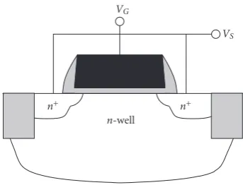
Figure 7: A sketch of ann-type (referring to the body doping) accumulation-mode varactor’s cross-section.
began to accommodate the accumulation-mode varactor [17,18] (Figure 7). This simplified the device bias scheme as compared to the more common inversion-mode varac-tor and simultaneously lowered its resistive losses and para-sitic contributions. As a frequency tuning element the advan-tages of the accumulation-mode varactor compared to the junction diode were clear, a largeCmax/Cminratio, an abrupt capacitive transition implying only the need for low tuning voltages, an isolated bias scheme, and acceptable Q. Opti-mization of these characteristics for LC-VCOs are straight-forward: one must increase the Cmax/Cmin, and reduce re-sistive losses. For parametric circuits a more detailed assess-ment is necessary.
First, unlike Manley-Rowe, a more accurate analysis of parametric circuit behavior must account for losses in the varactor. To this end a rough but physically realistic pumped varactor model employs a nonlinear capacitance in series with a resistance,Rs. As emphasized by Penfield and Rafuse [19] this varactor model sidesteps the difficulties and inac-curacies that emerge when a parallel RC equivalent is used or when the series resistance is incorporated into source and load impedances. The terminal characteristics of this physi-cally motivated model are best described with the relation
v(t)=
S(t)i(t)dt+Rs(t)i(t). (17)
This equation directly catalogues the influence of the pump voltage on the varactor as a whole. However, it contains a rel-atively obscure varactor measure, the incremental elastance,
S(t).1 A rough approximation of a MOS varactor elastance per unit area is given by
SVGS
=Qsd
VGS
esNd + 1
Cox, (18)
whereCoxis the oxide capacitance,eis the electronic charge, sis the permittivity of the semiconductor,Nd is the donor
doping in the semiconductor (a uniformly doped n-type accumulation-mode varactor is assumed), andQsdis the de-pletion charge in the semiconductor body. The dede-pletion charge itself is modeled semi-empirically with
Qsd= es
whereγis the device body factor and
VMOS=1
The above follows a modeling technique reported in [20] and, as in that work, incorporates a small smoothing factor,
δ. This correction is used since the transition from full accu-mulation to flat-band is not rigorously accounted for here. With such factors present it is best to consider this model as a rough design guide. A detailed account of the varactor de-vice physics in compact model form is described in [21] for example. The value of the simple model described here lies in its direct exposure of the relations between performance and device characteristics.Section 4.2discusses this, along with device losses, in detail.
A comparison of this approximation to the normalized CV and SV characteristics extracted from a full charge-based analysis [22] as well as a simple tanh curve fit is presented inFigure 8. As shown, the tanh curve, a popular approach in empirical compact CV models, underestimates the elastance in depletion. We return to this point inSection 4.2.
4.2. Figures of merit
The elastance characteristics must be considered along with device losses in estimating the impact of integrated MOS technology on parametric performance. Penfiled and Rafuse [19] highlighted two figures of merit, thecutofffrequency
fc=Smax−Smin
2πRs (21)
and themodulation ratio
mn= |Sn|
Smax−Smin.
(22)
The cutofffrequency, which we can express in more familiar varactor measures as
fc= Cmax−Cmin 2πRsCmaxCmin
, (23)
reflects only the influence that device properties bear on the circuit. Ideally, fc marks the maximum frequency at which it is worth pumping the capacitor. Conversely, the modula-tion ratio encompasses several contribumodula-tions. The numera-tor,|Sn|, indicates the size of the elastance harmonic at the pumping frequencyn·fp. That is, assuming small-signal con-ditions, we can treat the elastance as a linear time-varying component controlled by the pump
S(t)=
∞
n=−∞
Snej2πn fpt. (24)
This is the elastance analog to (8). The elastance harmonics are influenced by three things: the bias of the pumping sig-nal, the amplitude of the pumping sigsig-nal, and the steepness of the varactor’s elastance characteristics. The steeper the SV curve is, the more efficient the pump is in relaying its energy to the varactor. As shown in (18) and (19) a large impact on the abruptness of the elastance characteristic can be made by reducing the channel doping. This necessarily increases the series losses, but at a rate proportional toNd, while the SV slope increases withN2
d. Similarly, we can see from (19) that a decrease in the gate capacitance per unit area,Cox, also con-tributes to an improvement in the SV slope. This also comes with the benefit of allowing larger pumping signals to be ap-plied across the gate oxide.
These relationships run in a direction counter to the changes employed in scaling MOS devices. Nonetheless the variety present in most modern MOS technologies presents some room for optimization. For instance, many CMOS pro-cesses offer devices of various oxide thickness and channel doping. A plot of the SV characteristics extracted from S-parameter measurements on accumulation-mode devices in a 0.13μm-CMOS technology with varying channel doping and oxide thickness is shown inFigure 9. In this case only devices with a marginal difference in oxide thickness were examined. As expected, a lower channel doping results in a steeper SV characteristic. The measured 4-to-1 ratio between
Smax andSmin is about 2.5 times greater than that available from a junction diode. The two channel doping levels (nom-inal and high) are obtained by employing threshold adjust implants intended for the variety of NMOS and PMOS de-vices offered in the technology. Unfortunately, a fourth ex-periment employing one of the available counterdoping im-plants and intended to have the lowest channel doping was not correctly processed at the foundry. This, correctly com-bined with the thick-oxide option available in most CMOS technologies, constitutes the most direct approach to device customization for parametric circuit applications.
Of note in the measurement results is the manner in which the elastance characteristic saturates in the depletion region. This is a characteristic encompassed by the tanh fit example included in Figure 8 but not the basic model of (18). The disparity between the predicted and measured elas-tance characteristics at large depletion bias can be traced to the fact that the varactor measurements were done with a small-signal, high-frequency (5 GHz) perturbation atop a slowly stepped bias—a common high-frequency CV extrac-tion technique [23]. Such a set-up allows minority charge to respond to the bias settings thus preventing the onset of deep depletion as naturally included by the basic model. However, in parametric circuit applications we can expect a large-signal, high-frequency pump voltage to continuously excite the MOS varactor. Thus, the equilibrium bias condi-tions present during measurement hardly apply for pumped varactors. This supports the elastance predictions of the basic varactor model, but a convincing answer requires an analysis beyond the scope of this paper.
tanh fit
Full charge model Approximate model
1 0.5 0 0.5 1
VGB VFB(V)
0 0.1 0.2 0.3 0.4 0.5 0.6 0.7 0.8 0.9 1
C/
Cox
(a) Capacitance-voltage characteristics
tanh fit
Full charge model Approximate model
1 0.5 0 0.5 1
VGB VFB(V)
1 1.5 2 2.5 3 3.5 4 4.5 5
S/
Sox
(b) Elastance-voltage characteristics Figure8: Comparing the rough semi-empirical model to a complete charge-based description and a tanh fit.
High doping, nominaltox
Nominal doping, lowtox
Nominal doping andtox
1 0.5 0 0.5 1
VGS(V)
0.4 0.6 0.8 1 1.2 1.4 1.6
Elastanc
e
(1/pF)
Figure9: Elastance measurements for accumulation-mode varac-tors with varying degrees of channel doping in a 0.13μm-CMOS technology.
consideration must be given to the reduction of series losses as attested by (23). For designers, with little control over the varactor’s physical characteristics, layout becomes paramount here. Without considering special layout tech-niques (such as differential excitation [24]), four controls are available: gate length (Lg), gate width (Wg), finger number (Nf), and number of stripes/segments (Ns). These combine
to give an active varactor area ofLg·Wg·Nf·Ns. To clarify, a varactor consists ofNsstripes in parallel, each containingNf fingers, in turn, each finger has dimensionsWg andLg. We must consider what arrangement of these terms maximizes
fc. This requires finding the right balance between layout in-fluence on series resistance and capacitance properties.
The series resistance can be divided into two main con-tributors, one is a constant value and is associated with the silicided poly gate, contacts, and via resistance on the ter-minals. The other contributor is associated with the channel material and is bias, doping, and frequency dependent.
For the accumulation-mode varactor with one finger, its series RC components can be modeled as inFigure 10, where
Rcg andRcsd are the contact and via resistances on the poly gate and n+ diffusion pickups (source/drain), respectively, andRgis the gate polysilicon resistance. Underneath the gate, the channel resistance is denoted byRch, whileRwis the resis-tance of then+diffusion bulk pickups and the well.C
varis the equivalent series capacitance of each finger. The model of the varactor with multiple fingers is shown inFigure 11, where
Rs f gandRs f sdare the series resistance between two fingers. For the gate resistance, if the gate poly of each finger is joined from both sides of source/drain, the equivalent poly resistance of one finger is
Rg = 1
12·
Wg
Lg ·Rg−
sh, (25)
whereRg−shis the gate’s sheet resistance. On the other hand, for the channel and well resistance we have
Rch,Rw∝
Lg
Gate Rcg Rg Cvar Rch
Rw
Rcsd S/D
Figure10: Model of a single-finger varactor.
Rs f g R
cg Rg Cvar
Rch
Rw
Rcsd Rs f sd
Rs f g R
cg Rg Cvar
Rch
Rw
Rcsd Rs f sd
Gate S/D
. . .
. . . Figure11: Model of a parallel multiple-finger varactor.
Being lower doped and unsilicided, the sheet resistance of the well and bulk, Rch,w−sh, is greater than that of the polysili-con. This suggests that one would use the minimum chan-nel length to reduce the body contribution to the series re-sistance. However, due to their inverse dependence on finger dimensions some tradeoffbetween the influence of (25) and (26) on the series resistance is present. This tradeoffaffects the setting forWg andLg, but it is not the only considera-tion.
As shown in (23) we want to maximizeCmax, minimize
Cmin, and minimize Rs. Somewhat arbitrarily choosing a minimum practical value ofCmin=100 fF (in anticipation of parasitic effects and process variations) we are left to consider howLg,Wg,Nf, andNsinfluence the remaining two charac-teristics, obviously this complicates selection based purely on anRg-Rchtradeoff. For instance, minimizingLg·Wg maxi-mizes theNf·Nsproduct and therefore reducesRs, but at the cost of increasing the relative parasitic capacitance contribu-tion and hence a reduccontribu-tion inCmax−Cmin.
Another important consideration is the contact and in-terconnect resistance introduced between fingers (Rs f g and
Rs f sd in Figure 11) and stripes. This is often ignored when assessing device resistance, but can certainly be influential. WithRs f g andRs f sdthe equivalent resistance will not be re-duced simply as a function of 1/Nf. AsNf is increased the series resistance will eventually saturate due to the contribu-tions of the interfinger conneccontribu-tions,Rs f gandRs f sd.
Getting a sense of how the characteristicsLg, Wg,Nf, andNsinfluence fcis greatly aided by the availability of ver-ilogA based compact models such as the one described in [21]. Since these models account for both physical and lay-out characteristics a broad comparison between designs can
Table1: Cutofffrequencies for varactor withWg = 1μm,Lg =
0.24μm, and area=43.2μm2.
Nf Ns Cmax(f F) Cmin(f F) Rs(Ω) fc(GHz)
180 1 477.8 187.3 13.77 32.57
60 3 481.5 188.1 2.429 212.2
30 6 481.8 188.3 0.8025 641.5
15 12 482.3 188.7 0.508 1011
5 36 483.5 190 1.275 399
Table2: Cutofffrequencies for varactor withWg =1.41μm,Lg =
0.34μm, and area=43.2μm2.
Nf Ns Cmax(f F) Cmin(f F) Rs(Ω) fc(GHz)
90 1 475.8 147.5 7.281 102.2
45 2 476.3 147.8 2.777 267.5
30 3 476.5 147.8 1.538 482.8
15 5 476.8 148.1 0.7094 1045
5 18 477.5 149 0.9085 808.9
Table3: Cutofffrequencies for varactor withWg = 2μm,Lg =
0.48μm, and area=43.2μm2.
Nf Ns Cmax(f F) Cmin(f F) Rs(Ω) fc(GHz)
45 1 475.8 147.5 4.359 222.8
5 9 476.3 122.1 0.9787 982.9
15 3 477.5 123.5 1.266 754.4
be made. Employing empirically based compact models the
fcfor a variety of accumulation-moden-type varactors (ex-cited in a single-ended manner) is shown in Tables1–3. The total active area (Lg ·Wg ·Nf ·Ns =43.2μm2) is the only value that all designs have in common. It is chosen such thatCmin remains above 100 fF over the relevant region of operation (VGS ranges from−1 V to 1 V).Table 1 summa-rizes the results for varactors consisting of minimum unit area (i.e.,Wg·Lg) elements,Table 2shows the results for de-vices composed of twice the minimum unit area, andTable 3 summarizes the characteristics of varactors composed of four times minimum unit area elements. Note that all Rs have been calculated for 5 GHz excitations. A layout dependent self-resonance frequency could not be extracted as the model did not account for inductive parasitics although it should be noted that self-resonant frequencies do not necessarily pose a problem for parametric circuits. The self-resonant frequency can be exploited as one of the modes of interest in the para-metric circuit.
Wg=2μm,Lg=0.48μm
Wg=1.41μm,Lg=0.34μm
Wg=1μm,Lg=0.24μm
0 5 10 15 20 25 30 35 40
Ns
0 200 400 600 800 1000 1200
fc
(GHz)
Figure 12: Plot of varactor cutofffrequencies versus number of stripes for a 43.2μm2(total active area) varactor.
area shrinks, more devices in parallel imply a smaller total resistance. As can be seen in all cases, this is best achieved by keeping Nf and Ns on the same order. Unfortunately, the capacitance of small unit areas contains a higher relative proportion of parasitic capacitance. This lowersCmax−Cmin which ends up hurting the fc. Attempts to get around this by increasing the unit area will be frustrated by an increase in series resistance simply due to a decrease in the parallel con-nection count. The simulated cutofffrequencies associated with these varactors are plotted inFigure 12as a function of stripe count. As can be seen, fcis relatively forgiving of unit size, but quite sensitive toNf andNsdistributions.
Measured results are available to double-check the CV characteristics of the scalable varactor model. The experi-mental varactor design has unit widths and lengths of 5μm and 0.42μm, respectively, which are arranged intoNs = 5 parallel stripes ofNf = 20 gate fingers each. InFigure 13, the CV curve obtained from the model is plotted along-side the CV data obtained from a high-frequency (5 GHz) S-parameter characterization of the varactor. It is observed that the CV characteristic of the fabricated device matches very closely with the scalable model (at the frequency of ex-traction).
We will attempt to tailor this varactor design for para-metric circuits by changing the number of stripes from 5 to 1. The implications of this change on the device characteristics and USBUC and LSBDC are explored in detail inSection 5. Even though reducingNswill shift the CV curve down and decrease theCmax−Cmin (as shown inFigure 13),Cminhas also been reduced thus increasing fc. The large change in ca-pacitance characteristics fromNs = 5 toNs =1 affects the performance quality of the parametric converter but not the substance of its operation, unlike, for example, that of a VCO, whose center frequency and tuning range would be severely
Ns=1: model
Ns=5: measurement
Ns=5: model
1 0.5 0 0.5 1
VGS(V)
0 0.5 1 1.5 2 2.5
C
(pF)
Figure13: Comparison of measurement results to compact model predictions.
VG+ VCM +
+ Vtune+
Vtune
VG
Figure14: Schematic of common-mode cancellation varactor.
impacted. The only requirement imposed in this work is that
Cminexceed 100 fF, which has been satisfied.
4.3. Composite structures
n+ p+ p+ p+ n+ n+ n+ n+ p-well
Deepn-well
n-well
p-substrate
VDD Vtune+ VG+ Vtune+ VG Vtune+ VDD Vtune VG+ Vtune VG Vtune
Figure15: A sketch of the cross-section of a common-mode-cancellation accumulation mode varactor. Compare this to the schematic of this “device” rendered inFigure 14.
antiparallel connection (i.e., a pair of two-terminal asym-metrical devices connected in parallel, but with opposite ter-minal orientations) [26]; in practice, it isolates the diff er-entialVG node from the substrate losses. Isolating sensitive nodes from the substrate is much less of a concern in the case of an SOI technology, but it is essential in a CMOS tech-nology where such a load can severely degrade the tankQ
in LC-VCOs. A common-mode rejection varactor (CMRV) circuit, consisting ofn-type andp-type accumulation-mode varactors, can be realized in any CMOS technology with a deepn-well. The deepn-well doping is used to define an iso-latedp-well and hence thep-type accumulation mode varac-tor needed to complement then-type varactor. Further, it is possible that such a device can be tightly integrated into one composite structure as illustrated inFigure 15. As sketched, the device also takes advantage of a differential excitation lay-out to help reduce series losses.
At present, CMOS processes commonly includen-type accumulation-mode devices, however it is uncommon to find the p-type corollary needed in the CMRV. To approx-imate the properties of such a pair, the 2D device simulator, MEDICI, is employed. The construction of the hypothetical
p-type device is guided by the approximated doping levels of ann-type varactor available in a 0.13μm-CMOS technology. The doping levels are simply mirrored.
The CV characteristics obtained for then-type and p -type accumulation mode varactors using MEDICI are shown inFigure 16. Apparently, a relatively antisymmetric response is possible if matched doping levels are used in the two de-vices. Simulator mesh size limits required a separate analysis for each varactor flavour, nonetheless the results are expected to be indicative of the fully integrated device operation. The benefits that such a device brings to VCO phase noise behav-ior in the presence of extrinsic disturbances are discussed in Section 6.
5. PARAMETRIC CIRCUIT SIMULATIONS
5.1. USBUC
Although useful as a general guide, the predictions of the Manley-Rowe relations apply only to the case of a lossless reactance. Penfiled and Rafuse [19] emphasized the need to account for series varactor losses when evaluating parametric circuit performance. Following this work, the available gain
p-type n-type
1 0.8 0.6 0.4 0.2 0 0.2 0.4 0.6 0.8 1 VGS(V)
1 1.2 1.4 1.6 1.8 2 2.2 2.4 2.6 2.8
Capacitanc
e
(fF/
μ
m)
Figure16: Comparison of MEDICI simulated CV characteristics of matchedn-type andp-type varactors.
vG vp
Rs
ZG Filtered and pumped varactor two port
Zo
Figure17: The upper-sideband upconverter represented as a two port with ideal filters and series loss,Rsonly in the varactor.
of an USBUC treated as a two port (seeFigure 17) is given by
1
Ga =
ωs
m1ωc 2
ZG+Rs−jS0/ωs2
RsRG +
ωs
ωu
Rs+RG
RG (27)
assuming that only (angular) frequenciesωs,ωp, andωu =
the cutofffrequency (in rad/s asωc) and the modulation in-dex (m1) is clearly seen here. Expecting the USBUC to be used in a millimeter wave communicator transmit chain, we are most interested in the conditions necessary for maximum gain. From (27) we find that maximum available gain is
Ga,max=
when the jS0/ωsterm is resonated out and the generator re-sistance is set to
RG=Rs
The varactor structures described earlier (Figure 13) are now used to get a sense of the performance attainable by the USBUC. The simulated figures of merit for these de-vices are summarized in Table 4. A DC point (−200 mV) is chosen for the pump signal such that the device is bi-ased evenly betweenSmaxandSmin. Also, the figures are ex-tracted for a sinusoidal pump signal of 300 mV peak ampli-tude applied directly across the varactor (i.e.,−6.5 dBm from a matched 50Ωpumping source). This prevents the genera-tion of higher-order harmonics which, under the circuit con-ditions considered here, do not contribute any useful power gain and may actually decrease it.
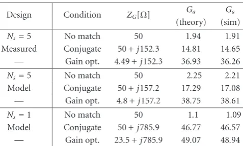
The simulation results for an USBUC that amplifies and converts a 1 GHz signal to a 60 GHz frequency are shown in Table 5. A number of conditions are examined and, for easy reference, compared to theoretical calculations of available gain. The results are determined for no input match ((27) withZG=50Ω), input conjugate match (ZG∗=Rs−jS0/ωs), and gain optimization “match” (28).
For the first two varactor simulations (Ns=5 measured and modeled), we see that the gain is well below that pre-dicted by the Manley-Rowe relations. We can attribute this to the fact that our upper-sideband frequency is greater than 0.427 (m1ωc)2/ωs(a design variable for USBUCs, indicating the signal frequency at which the converter’s available power gain begins to saturate [19]), in the case of the five-stripe varactor (i.e., measured and modeled). Therefore, this varac-tor is an unsuitable choice for the design we have presented, since we are pumping it at too high a frequency. The one-stripe varactor, with a composite merit figure (m1ωc) more than twice as great does not exceed the above condition and comes within 15% of the Manley-Rowe prediction.
5.2. LSBDC
Once again, following [19], for the LSBDC, considering var-actor losses, the exchangeable gain becomes
1
From this equation, we can see that it is possible for the avail-able gain to be negative. However, for this to be possible,
Table4: Relevant varactor measurements withVdc= −200 mV and
Vp=300 mV (peak).
Table5: Simulated USBUC power gain.
Design Condition ZG[Ω] Ga Ga
Assuming that one LSBDC will do the job of an entire re-ceiver front end (i.e., LNA, mixer, oscillator) its noise behav-ior becomes an important concern. The noise temperature of the LSBDC is given by
T=Td
whereTd is the varactor temperature. If we are planning on implementing this receiver system with an on-chip antenna, we can expect the antenna and the varactor to be roughly the same temperature. Thus the single-sideband noise factor will be
Table6: Simulated LSBDC performance.
Furthermore, the source resistance can be tuned to im-prove the noise factor even more. Setting it to
RG=Rs
results in an excess noise factor of
F−1= 2ωs
As for the gain of the LSBDC, when the noise is opti-mized, the available gain is predicted to be
Ga=
Thus, the available gain can still be negative under optimum noise matching conditions, implying that the LSBDC still has a negative equivalent output resistance and hence the abil-ity to deliver power at the signal and downconversion ports. Note that in this case (optimum noise match), it is possible to increase the gain by changing the pumping frequency and henceωd; this option is somewhat limited when the LSBDC serves as a downconverter (as opposed to a straight LNA) since the IF frequency is not commonly a design variable on the circuit level.
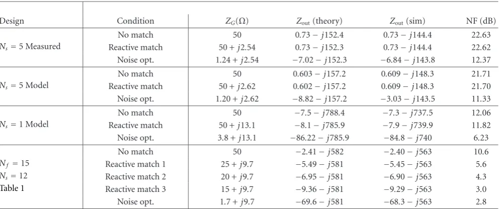
As done for the USBUC, we examine the (noise) perfor-mance of the LSBDC with the same varactor structures and pumping conditions summarized inTable 4as well as simi-lar operating conditions (60 GHz input signal, 1 GHz down-converted signal). InTable 6, the theoretical and simulated
output impedances along with the expected noise figure of each of the LSBDC circuits are given. Note that we present the output impedances as opposed to the available gain from the LSBDC. The reason for this is that the absolute value of gain can be smaller than one, yet gain will still be pos-sible, depending on the load. Thus if we know the output impedance of the LSBDC, we can choose the loads appro-priately to give the desired gain. Admittedly this is difficult to do in board-level designs, but certainly is not out of the question in high frequency integrated circuits where design-ers have much more control over the interface between cir-cuits. In the case of the five stripe varactor (measured and modeled), when the source resistance is 50Ω, the real part of the output impedance will actually be positive, and thus the LSBDC will operate with a power loss when using these varactors under the conditions in this analysis.
analysis considers only the varactor’s noise contribution, but it should be noted that the device under question is inferior to a number of other available device designs cataloged in Tables 1to 3. Optimizing around one of the better varac-tors listed (specifically, the minimum unit area varactor with
Nf = 15 andNs = 12 in Table 1) predicts very encourag-ing results for the operational circumstances under consider-ation. An optimum noise figure of 2.8 dB is predicted under an optimumRGof 1.7Ω. This value increases to 3, 4.3, and 5.6 dB at more reasonable source resistances of 15, 20, and 25Ω, respectively.
6. FREQUENCY CONTROL
A schematic of a simple cross-coupled CMOS LC-VCO structure is shown inFigure 18. The circuit incorporates the common-mode rejection varactor (CMRV) introduced in Section 4.3. Only one switching core is used to overcome tank losses, a PMOS cross-coupled pair. This allows the cir-cuit to operate with low voltage supply headroom. Also, buried channel PMOS devices are employed for their lower flicker noise contribution.
In this case, the purpose of the CMRV is to maintain the large tuning range inherent to MOS varactors while simul-taneously desensitizing the VCO to common-mode fluctua-tions induced by the supply noise. The CMRV allows a dif-ferential signal (e.g.,V+
tune−Vtune− ) to simultaneously excite then- andp-type varactors into their depletion or accumu-lation regimes. Meanwhile, a common-mode excitation (e.g.,
VCM) drives the two devices into opposite regimes of opera-tion, thus blunting the overall response of the CMRV to that signal.
A substantial source of common-mode noise in modern mixed-signal environments is the rail noise atVDDandVSS. The PMOS current mirror (M3−M4) helps block outVDD -noise. However, ordinarily, the phase noise performance of this topology would be severely compromised by variations onVSS. That is, any noise occurring onVSScan be expected to lead to a large increase in the VCO phase noise. A com-parison of this increase between a 5 GHz LC-VCO employ-ing an n-type varactor and an identical VCO employing a CMRV over a tuning voltage spanning−1V to 1V is shown in Figure 19. Specifically, the change in spot phase noise at 1 MHz removed from the center frequency is compared using the SpectreRF simulator. In both cases (i.e., normal and CMRV tuned VCO) uniform low-frequency noise (0 to 20 MHz) is placed onVDD andVSSand sized such that the common-mode noise density (in V2/Hz) induced by each noisy rail at a tank node is 70 dB greater than intrinsic VCO noise effect at that node. High-frequency extrinsic noise is less of a concern in this case as it can be more effectively sup-pressed by on-chip shunt capacitors.
ForVSSnoise (solid line inFigure 19) the CMRV offers a substantial improvement. At best, the 1 MHz spot phase noise is more than 50 dB less sensitive toVSS fluctuations on the CMRV tuned VCO. This occurs when the varactor is tuned within the CV transition region between accumu-lation and depletion regimes. Expectedly, asVtuneis changed
vnss
M4
vndd
M3
M2 M1
vcm
+ V+
tune
VCM
Vtune Vtune +
vnss
Figure18: A simple CMOS LC-VCO with common-mode cancel-lation varactor.
and the CMRV biased in one of its saturated domains the common-mode cancellation effect is diminished. For VDD fluctuations (dashed line inFigure 19) the CMRV offers little benefit in this topology. In this case, any noise that enters the common-source terminal of the cross-coupled PMOS pair throughM3 is converted to a differential form. As already stated, the CMRV does not filter out such excitations.
7. DISCUSSION
Customized varactor structures can help standard CMOS technology continue to meet more demanding RFIC chal-lenges. In this paper we discussed the role that these devices can play in assisting millimeter wave signalling and frequency control in a mixed-signal environment. The former is ad-dressed by suggesting the use of MOS varactors in parametric conversion circuits. This circuit approach is always an option when operational frequencies beyond the reach of transistor technology are the goal. The MOS varactor assists the effi -cacy of this technique with its rich nonlinearity (compared to the junction varactor), broad capacitive range, comple-mentary structure (i.e.,n-type andp-type varactor modes), three-terminal operation (not discussed in this paper), and unintrusive biasing.
VDDnoise
VSSnoise
1 0.8 0.6 0.4 0.2 0 0.2 0.4 0.6 0.8 1 Tuning voltage (V)
10 0 10 20 30 40 50 60
Phase
n
oise
ch
ange
(dB)
Figure19: Simulated change in phase noise for single-ended and common-mode reject varactor structure.
approaches are aided by IC implementations (better match-ing) and the custom device structures (complementary var-actors) which can be fabricated with only a layout rearrange-ment (i.e., without specific need for thermal budget or dop-ing adjustments durdop-ing processdop-ing). Suggestions were also made for customization of physical MOS varactor character-istics to better suit parametric needs. Given the availability of thick oxide analog devices in mixed-signal CMOS technolo-gies and the presence of multiple threshold implants even this adjustment can be implemented without significant pro-cess demands.
Attention was also brought to several issues involving accumulation-mode varactors in parametric converters. The importance of elastance-based design was mentioned (e.g., this influences the optimum pump biasing) and a simple elastance model discussed. An outstanding point is the im-pact of nonequilibrium, deep-depletion effects. RF MOS characterization typically does not elicit this behavior, how-ever it is expected to play a role in parametric circuit perfor-mance. An investigation into optimum device layout based on compact models highlighted the need to balance finger and stripe count of the varactor. Ignored were the possible influences of capacitive well parasitics on the frequency re-sponse of parametric ICs.
The effect of a complementary LC-VCO tuning scheme was also studied in simulation. A significant improvement in the ability of the circuit to block common-mode extrin-sic noise was noted. This approach can significantly blunt large low-frequency common-mode noise, but, is compro-mised by the single-ended-to-differential conversion proper-ties of the cross-coupled pair in differential VCOs.
REFERENCES
[1] M. Faraday, “On a peculiar class of acoustical figures; and on certain forms assumed by groups of particles upon vibrating
elastic surfaces,”Philosophical Transactions of the Royal Society of London, vol. 121, pp. 299–340, 1831.
[2] H. Suhl, “Proposal for a ferromagnetic amplifier in the mi-crowave range,”Physical Review, vol. 106, no. 2, pp. 384–385, 1957.
[3] M. T. Weiss, “A solid-state microwave amplifier and oscillator using ferrites,”Physical Review, vol. 107, no. 1, p. 317, 1957. [4] R. V. L. Hartley, “A wave mechanism of quantum phenomena,”
Physical Review, vol. 33, p. 289, 1929.
[5] R. V. L. Hartley, “Oscillations in systems with non-linear re-actance,”Bell System Technical Journal, vol. 15, pp. 424–440, 1936.
[6] W. Barrow, “On the oscillations of a circuit having a periodi-cally varying capacitance,”Proceedings of the Institute of Radio Engineers, vol. 22, pp. 201–212, 1934.
[7] J.-P. Raskin, A. R. Brown, B. T. Khuri-Yakub, and G. M. Rebeiz, “A novel parametric-effect MEMS amplifier,”Journal of Micro-electromechanical Systems, vol. 9, no. 4, pp. 528–537, 2000. [8] A. Olkhovets, D. W. Carr, J. M. Parpia, and H. G. Craighead,
“Non-degenerate nanomechanical parametric amplifier,” in Proceedings of 14th IEEE International Conference on Micro Electro Mechanical Systems (MEMS ’01), pp. 298–300, Inter-laken, switzerland, January 2001.
[9] S. Ranganathan and Y. Tsividis, “Discrete-time parametric amplification based on a three-terminal MOS varactor: anal-ysis and experimental results,”IEEE Journal of Solid-State Cir-cuits, vol. 38, no. 12, pp. 2087–2093, 2003.
[10] S. Knappe, V. Shah, P. D. D. Schwindt, et al., “A microfabri-cated atomic clock,”Applied Physics Letters, vol. 85, no. 9, pp. 1460–1462, 2004.
[11] J. M. Manley and H. E. Rowe, “Some general properties of nonlinear elements—Part I. General energy relations,” Pro-ceedings of the Institute of Radio Engineers, vol. 44, pp. 904–913, 1956.
[12] H. E. Rowe, “Some general properties of nonlinear elements. II. Small signal theory,”Proceedings of the Institute of Radio En-gineers, vol. 46, pp. 850–860, 1958.
[13] B. Kleveland, C. H. Diaz, D. Vock, L. Madden, T. H. Lee, and S. S. Wong, “Monolithic CMOS distributed amplifier and oscil-lator,” inProceedings of IEEE International Solid-State Circuits Conference, Digest of Technical Papers (ISSCC ’99), pp. 70–71, San Francisco, Calif, USA, February 1999.
[14] B. Hackl and J. Bock, “42 GHz active frequency doubler in SiGe bipolar technology,” inProceedings of International Conference on Microwave and Millimeter Wave Technology (ICMMT ’02), pp. 54–57, Beijing, China, August 2002. [15] C. Lee, T. Yao, A. Mangan, K. Yau, M. A. Copeland, and S.
P. Voinigescu, “SiGe BiCMOS 65-GHz BPSK transmitter and 30 to 122 GHz LC-varactor VCOs with up to 21% tuning range,” inProceedings of IEEE Compound Semiconductor Inte-grated Circuit Symposium (CSIC ’04), pp. 179–182, Monterey, Calif, USA, October 2004.
[16] H. Chan, “Sub-harmonic pumping in parametric amplifiers,” M.Sc. dissertation, University of Calgary, Calgary, Alberta, Canada, (in preparation).
[17] T. Soorapanth, C. P. Yue, D. K. Shaeffer, T. I. Lee, and S. S. Wong, “Analysis and optimization of accumulation-mode varactor for RF ICs,” inProceedings of IEEE Symposium on VLSI Circuits, Digest of Technical Papers, pp. 32–33, Honolulu, Hawaii, USA, June 1998.
Digest of Technical Papers, pp. 34–35, Honolulu, Hawaii, USA, June 1998.
[19] P. Penfield and R. P. Rafuse,Varactor Applications, MIT Press, Cambridge, Mass, USA, 1962.
[20] J. Maget, R. Kraus, and M. Tiebout, “A physical model of a CMOS varactor with high capacitance tuning range and its application to simulate a voltage controlled oscillator,” in In-ternational Semiconductor Device Research Symposium (ISDRS ’01), pp. 609–612, Washington, DC, December 2001. [21] J. Victory, Z. Yan, G. Gildenblat, C. McAndrew, and J. Zheng,
“A physically based, scalable MOS varactor model and extrac-tion methodology for RF applicaextrac-tions,”IEEE Transactions on Electron Devices, vol. 52, no. 7, pp. 1343–1353, 2005.
[22] Y. P. Tsividis,Operation and Modeling of the MOS Transistor, McGraw-Hill, New York, NY, USA, 1987.
[23] E. H. Nicollian and J. R. Brews,MOS (Metal Oxide Semicon-ductor) Physics and Technology, Wiley-Interscience, New York, NY, USA, 1982.
[24] A.-S. Porret, T. Melly, C. C. Enz, and E. A. Vittoz, “Design of high-Q varactors for low-power wireless applications using a standard CMOS process,”IEEE Journal of Solid-State Circuits, vol. 35, no. 3, pp. 337–345, 2000.
[25] S. Magierowski, K. Iniewski, and S. Zukotynski, “Differentially tunable varactor with built-in common-mode rejection,” in Proceedings of 45th Midwest Symposium on Circuits and Sys-tems, vol. 1, pp. 559–562, Tulsa, Okla, USA, August 2002. [26] R. G. Meyer and M. L. Stephens, “Distortion in
variable-capacitance diodes,” IEEE Journal of Solid-State Circuits, vol. 10, no. 1, pp. 47–54, 1975.
[27] B. A. Floyd, S. K. Reynolds, U. R. Pfeiffer, T. Zwick, T. Beukema, and B. Gaucher, “SiGe bipolar transceiver circuits operating at 60 GHz,” IEEE Journal of Solid-State Circuits, vol. 40, no. 1, pp. 156–167, 2005.
Howard Chanis currently completing his electrical engineering M.S. degree in the Department of Electrical and Computer Engineering at Schulich School of Engineer-ing at the University of Calgary. His research is focused on parametric converter IC de-sign.
Zhongbo Chen received his B.Eng. de-gree in electrical engineering from South-west Jiaotong University, Sichuan, China, in 1994. Currently he is pursing the M.S. degree in the Department of Electrical and Computer Engineering at the Schulich School of Engineeing at the University of Calgary, Canada. His research interests in-clude RFIC design with the emphasis on VCO noise analysis and surpression,
mod-eling of passive and active devices in deep-submicron CMOS tech-nologies. He is currently completing his electrical engineering M.S. degree in the Department of Electrical and Computer Engineering at the University of Calgary. His research is focused on the custom varactor designs for system-on-chip VCO ICs.
Sebastian Magierowskireceived the Ph.D. degree in electrical engineering from the University of Toronto and is currently an Assistant Professor in the Department of Electrical and Computer Engineering in the University of Calgary’s Schulich School of Engineering. His general research program is concerned with the realization of inte-grated wireless microsystems incorporating a wide variety of physical phenomena. More
specifically his group is defining advanced physical layer radio ar-chitectures accounting for all components between the antenna and channel coder. His industrial experience includes work at Nor-tel Technology in Ottawa focusing on RF MOS device modeling and high-speed mixed-signal design at PMC-Sierra, Inc., Burnaby, Canada. He is the cofounder of Protolinx, corp., a high-speed wire-less network start-up.
Krzysztof (Kris) Iniewski is an Associate Professor at the Electrical Engineering and Computer Engineering Department of Uni-versity of Alberta. His interests are in ad-vanced CMOS devices and RF circuits for wireless applications. His research program is to build “smart dust,” ultra low power ICs to be used in medical applications, wearable electronics, and ad hoc sensor networks. In addition to his academic duties he is a