IJEDR1602377
International Journal of Engineering Development and Research (www.ijedr.org)2148
High presentation of current differencing
transconductance amplifier and it’s relevance in
precision current-mode rectification
1Nidhi Pant,2Vishal Ramola 1M.Tech student,2Assistant Professor
1VLSI Design, Faculty of Technology, Uttarakhand Technical University ,Dehradun-248007, INDIA
________________________________________________________________________________________________________
Abstract - CMOS based circuit is demonstrated for the realization of the Current Differencing Transconductance Amplifier.The circuit which is projected in this paper can even offer the various benefits with the advantage of broad frequency bandwidth and extremely small input terminal impedance. The simulations and purpose has been illustrated to prove it’s remuneration and benefits of the circuit being projected for the means of precise high frequency alteration of the signal.
IndexTerms - Current Differencing Transconductance Amplifier,Digital Signal Processing,Current Differencing Buffered Amplifier
________________________________________________________________________________________________________
I.INTRODUCTION
It is well known that Current Differencing Transconductance Amplifier ie,CDTA was firstly invented by Biolek in the year 2003 which is liberated from parasitic input capacitances and it could be applied in variety of frequency assortment because of the current mode operation ability of the element. It’s block oriented structure is equivalent to CDBA element (Current Differencing Buffered Amplifier) , in which voltage unity gain buffer is used instead of the OTA.
Recently, an increasing number of analog circuits functioning in a current mode has been observed. The mounting interest in current mode analog circuits is caused by the exertion to diminish the supply voltage of the devices up to which it is possible which is especially important in transferable and battery powered apparatus. The bandwidth obtained for current mode circuits is usually higher than for voltage mode circuits created in the same technology.Although the CDTA can be constructed from commercially available integrated circuits, the precise, fast, and temperature-independent applications require utilizing a CDTA chip, implemented in the CMOS or bipolar technology.CDTA may be applied in the CMOS as well as the bipolar technologies. The first published CMOS realization of the CDTAas well as another topology presented in utilized 0.5 _m CMOS MIETEC process by means of ±2.5V supply voltages. The workpresents the so-called MOCDTA (Multiple Output CDTA) as an extension of the innovative circuit structure fromby additional current outputs. The CMOS structure reported in [6] can operate in supply rails down to ±0.75 V, utilizing the 0.35 um AMIS technology.
II.PERFORMANCE OF CDTA
DSP is becoming increasingly more powerful while advances in IC technology provide compact efficient implementation of its algorithms on silicon chips. Although many types of signal processing have indeed moved to digital domain, analog circuits are fundamentally necessary in many of today’s complex, high performance systems. This is caused by the reality that naturally occurring signals are analog. Therefore analog circuits act as a bridge between the real world and digital systems. In the beginning, operational amplifiers were the main building blocks for analog circuit design. Unfortunately, their limited performance such as bandwidth,slew-rate etc. led the analog designer to search for other possibilities and other building blocks. Proper symbol of the element called CDTA can be seen in fig.1 with the corresponding circuit of CDTA is described in fig.2
IJEDR1602377
International Journal of Engineering Development and Research (www.ijedr.org)2149
The connection between the terminals of CDTA could be characterized and are explained as follows:n p z n p
i
i
i
v
v
0
z Z m z m z z z m z mx
g
v
g
Z
i
i
g
v
g
Z
i
i
,
(1)By going through the above relations between the characteristic equations it can be said that p,n will be the terminals of input and ZZ would be the external impedance associated at the next port named as ’Z’.The difference of the current will be folled by the current source for the particular application which would be done between the two terminals p and n respectively which makes it’s way from Z port to the impedance ZZ.The terminal z suffers from the voltage drop and thus drop of voltage is given away to the x port which will have certain current in it which is denoted by ix. from the transconductance gain denoted by gm.This will be opportunate by electronic means subsequently to the outside bias current.CDTA is a self possessed device of unity gain source of current and there are two inputs to the current and amny outputs to the transconductance amplifier so that the modifications could be made by the means of electronics by the itinerary of the gain of transconductance offered by the device for the particular application. This has made our experiments very easy and the device proper appropriate in favor of the production of current-mode filters in the midst of electronically tenability characteristics.Additionally,this device could be used in many applications so that the whole experimental results could be found out for the production of filters made on the basis of their current mode operation.
Fig.2 Equivalent model of CDTA[21]
With a rigorous quantity of acquiescent fundamentals the required block can therefore make it able to perform in that particular environment. By this way the thick and strong blocks could be achieved in variety of experiments in the practical manner.The elemnt CDTA becomes forthcoming in many ways so as to realize the continuous processing of the signal of time repeatedly in all the equipments one after other without any disturbances.
Behaviour of CDTA
Every electronics element shows ideal and practical behaviour.current differencing transconductance amplifier also shows ideal and practical behaviour.From matrix equation (1.4) and (1.5) we can get the ideal and practical behaviour of CDTA.The principle performance may be elaborated as follows:
z m x n p
Z
I
I
I
g
V
I
,
(2)Practical behaviour associated with CDTA is described as follows:
Z m x n n p p
z
I
I
and
I
g
V
I
(3)
current gains are defined by αpand αn, αp= 1 - εp, and αn= 1 - εn. their complete ideals which are greatly less than the unity.
III.MOS-BASED CDTA IMPLEMENTATION
IJEDR1602377
International Journal of Engineering Development and Research (www.ijedr.org)2150
Fig.3 CMOS-based CDTA implementation[1]IV.PRECISION RECTIFIER USING CDTA
This defines high performance CDTA and it’s function within precision current mode rectification. The figure3. properly describes the current mode full wave rectifier which is utilized only by the means of a CDTA.The documented customary of the alteration of element may be visualized with the help of representation of the required circuitry.Now the main thing is to place single CDTA instead of two positive current conveyors.The gain of current is positioned by the external resistance R and the value of R will be taken as 1/gm .In order to get a unit gain current the gain could be furthermore be proficiented by just making it free from the resistor and the auxiliary current can be injected into the terminal.If the DC value is appropriately handled and applied the current tracking errors and the offsets of current that causes some DC imperfections.The enduring element of the rectifier that is diodes and the Rload.Also bias circuitry is examined throughly and specified properly.When it is to be chosed between the off and on conditions of current Iaux that causes some DC imperfections.The enduring element of the rectifier that is diodes and the Rload.Also bias circuitry is examined throughly and specified properly. To get rid of the postponement awakened by diodes at the same time as switching between the ON and OFF conditions and numerous kinds of DC biasing can take place into the account of the desired representation and it’s behavior.
Fig.4 Full-wave rectifier based on current mode circuit where resistor R could be absent[1]
V.RESULT
A high performance CDTA with it’s application in precision current mode rectification is defined and explained in this section. Simulations of the projected CMOS CDTA and precision rectifier could be prepared by means of PSPICE with TSMC 0.35µm n-well CMOS procedure. Power supplies are chosen as Vdd = −Vss = 1.8V. The dimension of the M12 is not equal to that of the M11 to terminate the increasing error. M21 has not the equivalent size with M23; and M26 has not the similar size with M25, M27, and M28 to abandon offset and level-shift errors. Bias current IB is elected as 40µA. The projected CDTA shows the mechanism near the GHz range. Figure. 3.8 shows the −3 dB bandwidths of the current gains Ix+/(Ip− In) and Ix−/(Ip− In),that are positioned at 1011MHz and 1230MHz correspondingly, for Rz = 1160Ωand In = 0A. The transconductances gm of DO-OTA for Vz= 1V DC are 873 and 882µA/V for Ix+/Vz and Ix−/Vz, correspondingly. and 882µA/V for Ix+/Vz and Ix−/Vz, correspondingly.
IJEDR1602377
International Journal of Engineering Development and Research (www.ijedr.org)2151
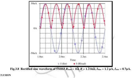
Fig. 5– AC simulation outcomes of CDTA designed for Ix+ / (Ip - In) and Ix- / (Ip - In) for RZ = 1160ΩIf the output of the waveforms are considered and we wish to improve those characteristics then definitely the diode characteristics will define the performance and to improve or to degrade both is in the hands of the self motivated diode which would not be present in the CDTA.The exceptional presentation can be seen having 5MHz of frequency..
Fig.3.8 Rectified sine waveform of 5MHZ Rload = 1Ω, R = 1.21kΩ, Ibias = 1.2 µA, Iaux = 0.7µA.
VI.CONCLUSION
In this study, a novel precision rectifier circuit using a performance CMOS-based CDTA structure is presented.The high-performance CMOS-based CDTA organization takes advantage for the huge bandwidth and close-to-ideal terminal impedances. The proposed circuit is suitable for monolithic integrated circuit implementation. CDTA-based precision full-wave rectifier described in this study is highly successful in high frequency procedure just because of the environment shown by current-mode operation.
VII.REFERENCES
[1]D.Biolek,V.Biolkova,“High-performance current differencing transconductance amplifier and its application in precision current mode rectification”,In:Proc. of the ECCTD’03, Krakow, Poland,Vol. III, pp.397-400, 2003.
[2]A.Sedra,K.C.Smith,“A second-generation current conveyor and its applications,” IEEE Transactions on Circuit Theory, Vol. 17, pp. 132-134, 1970.
[3]A.T.Bekri,F.Anday,“Active Filter Design Using Current Differencing Transconductance Amplifiers”,Int. ConFerence Applied Electronics, Pilsen, Czech Republic, pp. 11-15,2004.
[4]A.U. Keskin and D. Biolek, “Current mode quadrature oscillator using current differencing transconductance amplifiers (CDTA)”, Circuits, Devices and Systems, IEE Proc. 1, 214–218 (2006).
[5]A.Uygur,H.Kuntman, and A.Zeki,“Multi-input multi-output CDTA-based KHN filter”, Proc ELECO 2005: The 4th Int. Conference on Electrical and Electronics, Bursa, Turkey, pp. 46-50,2005.
IJEDR1602377
International Journal of Engineering Development and Research (www.ijedr.org)2152
[7]A.Uygur,H.Kuntman, “Design of a current differencing transconductance amplifier (CDTA) and its application on active filters”, Proceedings of the IEEE Signal Processing and Communication Applications Conference, pp. 340 – 343,2005.[8]DT.Comer,DJ.Comer,JR.Gonzales,“CDTA based transimpedance type firstorder all pass filter”, IEEE Trans Circuit Syst -II,Vol.44, pp. 856-60,1997.
[9]D. R. Frey, Log-domain Fltering: an approach to current mode Fltering," IEE Proceedings Circuits, Devices and Systems, Vol. 140, No. 6, pp. 406-416, 1993.
[10]K.Smith,A.Sedra,“The current conveyor - a new circuit building block”, IEEE Proc., Vol. 56, pp. 1368-1369,1968.
[11]M.Higashimura, Y.Fukui, “ Realization of all pass and notch filters using a single currentConveyor”, International Journal of Electronics,Vol. 65, No.4, pp. 249-50,1998.
[12]M.Siripruchyanum,W.Jaikla,“CMOS current-controlled current differencing transconductance amplifier and applications to analog signal processing,”Int. J.Electron.Commun.(AEU),Vol.62,pp.277- 287,2008.
[13]M.T Abuelmaatti, ., &M.H Khan. (1996). Grounded capacitor oscillators using a single operational transconductance amplifier.Active and Passive Electronic Components, 19, 91–98.
[14]M.Bhushan, & R. W. Newcomb, (1967). Grounding of capacitors in integrated circuits. Electronics Letters, 3, 148–149. [15]M.T Abuelmaatti,., & H.A Al-Zaher. (1999). Current-mode sinusoidal oscillators using single FTFN. IEEE Transactions on Circuits and Systems-II, 46, 69–74.
[16]M.Siripruchyanun,W.Jaikla,“ Realization of Current Controlled Current Differencing Transconductance Amplifier (CCCDTA) andIts Applications”, ECTI Trans. On El. Engg,Electronics and Comms., Vol. 5, No. 1, pp. 41-50.2007.
[17]N.A.Shah,M.Quadri,S.Z.Iqbal,“Current mode multifunction filter using current differencing transconductance amplifier”, Indian Journal of pure & applied physics, 45, 9, Sept. pp. 767-769,2007.
[18]S.Kilinc, Jain,V.Aggarwal , & U.Cam (2006). Catalogue of variablefrequency and single-resistance-controlled oscillators employing a single differential difference complementary current conveyor. Frequenz, 60, 142–146.
[19]T.Kaulberg,“A CMOS current-mode operational amplifier,” IEEE J. Solid-State Circuits, Vol. 28, pp. 849-852,1993.
[20]Tangsrirat,W.Dumawipata,T.Surakampontorn,“Multiple-input single outputcurrent-mode multifunction filter usingcurrent differencing transconductance amplifiers”, Int. J. Electron. Commun. (AEÜ),Vol. 61, Issue 4, 2007, pp. 209-214.