Comparative Analysis of Performance of
7- Segment Display Using Different Low
Power VLSI Designs
Rajdeep Chahal
1, Pritam Barua
2, Puja Sarkar
3, Debika Chaudhuri
4, Atanu Nag
5, Sukanta Bose
6.
4th Year Student, Department of ECE, Modern Institute of Engineering & Technology, Bandel, West Bengal, India 1-3,
Assistant Professor, Modern Institute of Engineering & Technology, Bandel, West Bengal, India 4,5,
CEGESS, BESU, Shibpur, West Bengal, India 6.
ABSTRACT: In applied physics, an adiabatic process is defined as any process that is asymptotically isentropic (thermodynamically reversible), that is, whose total entropy generated tends towards zero in some appropriate limit (typically, of low speed and/or improved isolation of the system). As for example asymptotically reversible heat engines were first described by Carnot in 1825 [1], which shows maximum possible thermodynamic efficiency. Part of the cycle of Carnot‘s engines involved processes with no heat flow, and this lack was the original and literal meaning of the term ― Adiabatic ―. But today, we would call the entire Carnot cycle adiabatic, in the more general applied physics sense of term, which has departed from the literal meaning. The field of ― Adiabatic Circuits ―[2] applies the general concepts of adiabatics to the design of Low-power electronic circuits in particular, consisting primarily today of digital MOSFET- based switching circuits[3].
Demands for low power and low noise digital circuits have motivated VLSI designers to explore new approaches to the design of VLSI circuits. Energy recovering logic is a new promising approach, which has been originally developed for low power digital circuits [4]. Adiabatic circuits achieve low energy dissipation by restricting current to flow across devices with low voltage drop and by recycling the energy stored on their capacitors [1].
Using this logic and its modification we have developed 7 segment display for digital combinational circuit design.
KEY WORDS: Adiabatic Logic. ECRL, Modified ECRL, 7-segment display, power, delay.
I.INTRODUCTION
To reduce the dissipation, the circuit designer can minimize the switching event, decrease the node capacitance, reduce the voltage swing, or apply a combination of these methods. Yet in all these cases, the energy drawn from the power supply is used only once before being dissipated. To increase the energy efficiency of logic circuits, other measures can be introduced for recycling the energy drawn from the power supply. A novel class of logic circuits called ―Adiabatic Logic‖ offers the possibility of further reducing the energy dissipated during switching events, and the possibility of recycling, or reusing, some of the energy drawn from the power supply. To accomplish this goal, the circuit topology and the operation principles have to be modified, some time drastically. The amount of energy recycling achievable using adiabatic technique is also determined by the fabrication technology, switching speed, and voltage swing.
II.ADIABATIC SWITCHING
A.CONVENTIONAL CHARGING :
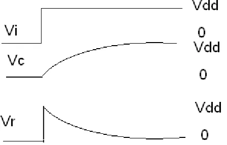
Fig 1: A static CMOS inverter and its equivalent circuit for the case where the Capacitor C is being charged through a device of on resistance R.
Fig 2: Voltage waveforms present in the equivalent circuit when charging the capacitor from 0 to Vdd in a conventional manner.
Fig 1 shows the voltage waveforms present when the input of the inverter swings from high to low, causing the capacitor C to being charging. At the instant of switching, the full supply potential appears across the on-resistance R of the p-type device , the waveform then decays as the capacitor is charged to Vdd. To charge the signal node capacitance C from a supply of potential Vdd, a charge q = CVdd is taken from the supply through the p-type device. The total energy Et
Then Et = qVdd
Or, Et = CVdd ² ………( 1 )
One half of the energy is applied to storing the signal on the capacitor and the other ½CVdd ² is dissipated as heat, primarily in the device on resistance R. Note that the dissipation is independent of this resistance, it is a result of the capacitor charging being obtained from a constant voltage source Vdd.
B. ADIABATIC CHARGING :
Fig 3: Voltage waveforms present in the equivalent circuit when charging then capacitor from 0V to Vdd in an adiabatic manner.
Adiabatic switching can be achieved by ensuring that the potential across the switching devices is kept arbitrarily small. In Fig 2 it can be seen that the potential Vr across the switch resistance is high in the conventional case because of the abrupt application of Vdd to the RC circuit.
Adiabatic charging may be achieved by charging the capacitor from a time varying source as shown in Fig 3. This source has an initial value of Vi= 0V – the ramp increases towards Vdd at a slow rate that ensures Vr= Vi-Vc is kept arbitrarily small. This rate is set by ensuring that the period of the ramp T >> RC.
In fact, the energy dissipated is,
Ediss = I ² RT = (CVdd/ T) ² RT=(RC/T) CVdd ² ……….(2)
A linear increase in T causes a linear decrease in power dissipation. Adiabatic discharge can be arranged in a similar manner with a descending ramp.
Now, if T sufficiently larger than RC, energy dissipation during charging Ediss —>0, and so the total energy removed from the supply is ½CVdd ²— the minimum energy required to charge the capacitor and hence hold the logic state . This energy may be removed from the capacitor and returned to the power supply adiabatically by ramping Vi back down from Vdd to 0V. As a result , given a suitable supply, it should be possible then to charge and discharge signal node capacitances with only marginal net losses.
Note that the RC time constant of a typical CMOS process is about 100ps. If we set T to ten time constants, the resulting delay though an adiabatic gate would be 1ns.
Although adiabatic circuits consume zero theoretically, they show energy loss due to nonzero resistance in the switches. The previous adiabatic circuits deliver energy in precharge phase, and recover their energy during the evaluation phase. The adiabatic circuits which uses diode-like devices for precharge causes unavoidable energy loss due to the voltage drop across the diode .
III.BASIC OPERATION OF ECRL
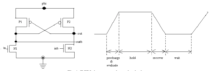
. Fig 4: ECRL inverter and supply clock
Generally ECRL circuits are consists of a block.The upper block consists of a PMOS transistors are cross coupled and are connected to the supply clock (1). And in the lower defines the logic which should be implemented. So the upper
block is responsible for charge recovery and the lower portion is responsible for logic defining.
For the purpose of initial discussion, let us assume ‗in‘ is at high and ‗inb‘ is at low. At the beginning of a cycle, when the supply clock 1 rises from zero to Vdd, out remains at ‗‘ as ‗in‘ turns on N2 and ‗out b‘ follows 1
through P1. When 1 reaches Vdd, the outputs hold valid logic level that is out=0 and out b=Vdd or logic 1. So, inversion
operation is performed. These values are maintained during the hold phase and used as inputs of evaluation of the next stage. After the hold phase 1 falls down to ground level, out b mode returns its energy to 1 so that the delivered charge
is recovered. Thus the clock 1 acts as both a clock and power supply.
So, it is seen from the description that P1 and P2 are used for charging the output nodes according to the
logic implemented in the lower block of the ECRL circuit. When the supply clock rises and are used for discharging a recover the charge from the output nodes to the supply clock when the supply clock falls.
Finally in the perspect of Energy loss, ECRL circuit‘s energy loss per cycle is EECRL= (2RPCL/T) CLVdd
2
+CLVTP 2
………. (3)
Where CL is the load capacitance, RP is the turn on resistance of PMOS, T is the transition time of the power clock, VDD
is the peak voltage of the power clocks, and VTP is the threshold voltage of the PMOS. In equation (3) the first term
represents the full adiabatic energy loss, and the second term represents the non-adiabatic energy loss.
As it can be seen from the fig 4, P1 and P2 transistor are responsible for recovering the charge from the output node to
the supply clock. And if we see eqn. (3), there for both the adiabatic and non-adiabatic loss p1 and p2 are responsible.
So, if we now put another N3 and N4 transistor by shorting their gate and the source, then they will behave like two extra resistors connected parallely to P1 and P2 and two extra path are created to recover the charge from the output
nodes to the supply clock.
From our basic circuit theory concept we know that if 2 resistors are connected parallel to each other then their equivalent resistance will be lower than smaller resistance among those 2. So energy dissipation will be lower also. Now this proposed circuit has the energy dissipation.
EECRL(proposed)= {((2.RPRN/RP+RN)CL)/T}CLVdd2+CLVTP2VTN2 ……(4)
By examining equation (4) we can see that both the adiabatic loss and the non-adiabatic loss become lower than the previous case.
We can also verify our proposal by simulating different gates constructed both by ECRL and proposed ECRL circuit design methods in next section.
V.BASIC GATES
Operation of AND Gate:
Fig 6: AND Gate by Proposed modified ECRL.
Operation of OR Gate:
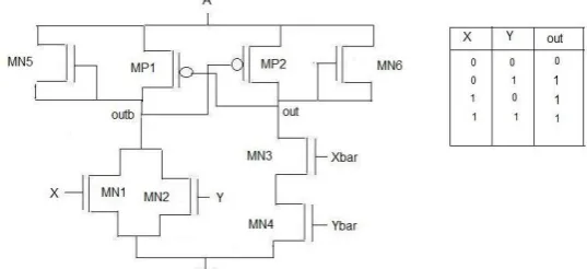
Operation of XOR Gate:
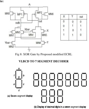
Fig 8: XOR Gate by Proposed modified ECRL
VI.BCD TO 7 SEGMENT DECODER
Fig 9: 7 segment display
By solving the expression of a,b,c,d,e,f,g using K-map we finally can design the decoder logic circuit.
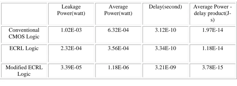
VII.RESULTS & DISCUSSION
The observed results are shown in Table I. From the analysis it is clear that BCD-to-7-segment decoder with modified ECRL logic is a good choice for low power and delay.
TABLE 1:
COMPARISONS FOR 7 SEGMENT DECODER OF 3 DIFFERENT LOGIC
Leakage Power(watt)
Average Power(watt)
Delay(second) Average Power - delay
product(J-s)
Conventional CMOS Logic
1.02E-03 6.32E-04 3.12E-10 1.97E-14
ECRL Logic 2.32E-04 3.56E-04 3.34E-10 1.18E-14
Modified ECRL Logic
3.39E-05 1.18E-06 3.21E-09 3.78E-15
VII.CONCLUSION
Till date most adiabatic logic families proposed have been relatively short-sighted, in view of the requirements for cost-efficient computing in the long run, which will require closely approaching the real physical limits of computing, in particular the need for near-total physical reversibility of the computing mechanism. These requirements preclude the use of diodes in adiabatic logic circuit designs. Attention must be paid to the current-carrying state of transistors at times when the devices being switched off, as well as the voltage state when the devices are switched on. Meeting all those requirements designs become an absolute economic necessity in the coming century , as the technology progresses day by day in the field of adiabatic circuitry we hope this logic will be predominant over other logic circuitry.In this conjunction our Modified ECRL logic shows significant energy saving compared with conventional CMOS logic and existing ECRL logic. It consumes less power and eventually delay is also less which is shown by using the simulation results (Tanner spice 14) to support our demands.
REFERENCES
[1] Sadi Carnot, Reflection on the Motive Power of Heat, Bachelier, Paris, 1825. http:// www. History .rochester.edu/steam/carnot/1943.
[2] W.C. Athas, L.J. Svensson, J.G. Koller, N.Tzartzanis, and Y.Chow.‖Low Power Digital Systems Based on Adiabatic Switching Principles‘‘ IEEE Trans, VLSI Systems, vol.2 no.4 pp.398-406 Dec 1994.
[3]‖CMOS Digital Integrated Circuits, Analysis & Design‘‘ Sung-Mo-Kang, Yusuf Leblebici, Tata-McGrow Hill, 3rd Edition
[4] S. Kim and M.C. Papaeftlymiou, ― True single-phase energy recovering logic for low power, high speed VLSI‘‘, Proc. Int. Symp low power Electronics and Design,pp 167-172, Aug 1998
[5] R.Downing, P. Gebler and George Katopis, ―Decoupling Capacitors effects on switching noise‖ IEEE Trans. Components, Hybrids and Manufacturing Technology, vol 16 no 5 pp 484-489, Aug 1993.
[6] Luns Tee, Lizhen Zeng, ―Charge Recovering Clocking for Adiabatic Style logic‖.
[7] kramer, A. Denker, J.S. et al.: 2nd order adiabatic computation with 2N-2P and 2N-2N2P logic circuits Proc. Intern. Symp. Low power Design 1995, pp 191-196. [8] Younis, S., Knight,T.: Asymptoticallyzero energy split-level charge recovery logic. Proc. Workshop Low Power Design, Napa Valley, California 1994, pp, 177-182. [9] Ye, Y. Roy, K.: Energy recovery circuits using reversible and partial reversible logic. IEEE Trans. Circuits Syst.I, vol. 43, Sep,1996,pp. 769-778.
[10] Moon, Y.,Jeong, D.-K.:An Eficient Charge Recovery Logic Circuit. IEEE Journal of Solid-State Circuits, vol. 31,196,pp.514-522.
[11] Lim, J., Kim,D.-G et al.: nMOS reversible energy recovery logic for ultra low energy application. IEEE J. Solid- State Circuits, vol 35, Jun 2000,pp 865-875. [12] Vetuli, A., Di Pascoli, S., Reyneri, L.M.,: Positive Feedback in Adiabatic Logic. Electronic Letters, vol. 32, No. 20, Sep 1996, pp. 1867ff