University of Windsor University of Windsor
Scholarship at UWindsor
Scholarship at UWindsor
Electronic Theses and Dissertations Theses, Dissertations, and Major Papers
1-1-1987
VLSI design of high-speed adders for digital signal processing
VLSI design of high-speed adders for digital signal processing
applications.
applications.
Seyfollah Seyfollahi Bazarjani
University of Windsor
Follow this and additional works at: https://scholar.uwindsor.ca/etd
Recommended Citation Recommended Citation
Bazarjani, Seyfollah Seyfollahi, "VLSI design of high-speed adders for digital signal processing applications." (1987). Electronic Theses and Dissertations. 6804.
https://scholar.uwindsor.ca/etd/6804
This online database contains the full-text of PhD dissertations and Masters’ theses of University of Windsor students from 1954 forward. These documents are made available for personal study and research purposes only, in accordance with the Canadian Copyright Act and the Creative Commons license—CC BY-NC-ND (Attribution, Non-Commercial, No Derivative Works). Under this license, works must always be attributed to the copyright holder (original author), cannot be used for any commercial purposes, and may not be altered. Any other use would require the permission of the copyright holder. Students may inquire about withdrawing their dissertation and/or thesis from this database. For additional inquiries, please contact the repository administrator via email
VLSI DESIGN OF HIGH-SPEED ADDERS
FOR
DIGITAL SIGNAL PROCESSING APPLICATIONS
by
Sey-follah Seyfol 1 ahi Bazarjani
A Thesis Submitted to the
Faculty of Graduate Studies and Research through the Department of
Electrical Engineering in Partial Fulfillment of the requirements for the Degree
of Master of Applied Science at the University of Windsor
W i n d s o r , Ontario, Canada
UMI Number: EC54793
INFORMATION TO USERS
The quality of this reproduction is dependent upon the quality of the copy
submitted. Broken or indistinct print, colored or poor quality illustrations
and photographs, print bleed-through, substandard margins, and improper
alignment can adversely affect reproduction.
In the unlikely event that the author did not send a complete manuscript
and there are missing pages, these will be noted. Also, if unauthorized
copyright material had to be removed, a note will indicate the deletion.
U M I ”
UMI Microform E C 54793 Copyright 2010 by ProQuest LLC
All rights reserved. This microform edition is protected against unauthorized copying under Title 17, United States Code.
ProQuest LLC
789 East Eisenhower Parkway P.O. Box 1346
S
"32-'2-Seyfollah Seyfol1ahi Bazarjani
(g) 1987
ABSTRACT :
In this work the VLSI design and implementation of high
speed arithmetic circuits for digital signal processing
applications, using the Residue Number System, is
investigated. Different techniques for high-speed Binary and
RNS arithmetic implementation are discussed. It will be
shown that for high-speed, high-precisi on arithmetic
computations, pipelined RNS adders offer advantages over
their binary counterparts. These advantages manifest
themselves in throughput rate, latency time, hardware
complexity, and testability.
Various CMOS logic families are presented. Charge
redi stribution problems in DOMING and DCVSL are addressed
and some techniques to alleviate these problems are studied.
Delay time analysis of Sample— Set Differential Logic, which
has not yet appeared in the literature, is described and an
analytical expression for the delay time of an SSDL gate is
derived. This expression is applied to the delay time
optimization of SSDL gates. The application of SSDL in
pipelined archi tectures is presented along with a
ACKNOWLEDGEMENTS
My Thanks and sincere appreciation is directed especially to
Dr. G.A. Jullien for his guidance, support and creative
suggestions. I am also thankful to Dr. W.C. Miller for his
s u p p o r t . I would also like to thank Dr. S. Bandyopadhyay,
TABLE OF CONTENTS
Page
A B S T R A C T ... iv
ACKNOWLEDGEMENTS ... v
LIST OF ILLUSTRATIONS ... ix
LIST OF APPENDICES ... xiii
CHAPTER 1 INTRODUCTION 1.1 Introduction ... 1
1.2 Computer Aided Design Tools Utilized 3 1.3 Objectives ... 4
1.4 Thesis Organization ... 4
CHAPTER 2 LOGICAL DESIGN OF BINARY ARITHMETIC CIRCUITS u^2.1 Introduction ... 7
t/2.2 Logic Design of Basic Binary Adder (Subtractor ) 7 U 2 . 3 High-Speed Adders ... 13
Lx2.3. 1 Carry Look-Ahead Adder ... 13
t ^ . 3 . 2 Ripple Carry Look-Ahead Adder 15 3. 3 First-Order Carry Look-Ahead Adder ... 19
\y2.3.4 Carry Select Adder ... 21
2.4 Parallel Multiplier ... 23
2.5 Pipelined Arithmetic ... 25
2.5.1 The Concept of Pipeline System 25 2.5.2 Pipelined Carry Save Adder 29 2.5.3 Pipelined Ri pple-Carry Adder 29 2.5.4 Pipelined Carry Look-Ahead Adder 29 2.5.5 Pipelined Multiplier ... 35
CHAPTER 3 RESIDUE ARITHMETIC AND DESIGN OF HIGH-SPEED
RNS ADDER
3. 1 Introduction ... .
3.2 Residue Re p ré s en t ât ion ...
3.3 Residue Arithmetic ...
3.4 VLSI Implementation of RNS Adders
3.4.1 Binary-Based RNS Adder
3.4.2 Look-Up Table RNS Adder 3.4.3 Hybrid Method ... . 3.4.4 Counter-Based RNS Adder 3.5 Pipelined Ripple-Carry RNS adder 3.6 Comparison of the Pipelined Ripple
Carry Binary and RNS Adder ...
3.6.1 Hardware Complexity ... 49
3.6.2 Throughput Rate ... 50
3. 6. 3 Test ab ili ty ... 51
3.6.4 Laten cy Time ... 52
3.7 Example ... 52
3.8 Summary ... 53
CHAPTER 4 CIRCUIT AND LOG IC DESIGN WITH CMOS 4. 1 Introduction ... 55
4.2 CMOS Logic Techniques .... 55
4.2.1 Static CMOS Complementary Logic 56 4.2.2 Pseudo-NMOS Logic ... 57
4.2.3 Pass-Transistor Logic ... 60
(Transmission Gate) 4.2.4 Clocked CMOS Logic ... 62
u ^ . 2 . 5 Basic Dynamic CMOS Logic ... 65
2.6 Domino CMOS Logic ... 71
^ . 2 . 7 NORA CMOS Logic (N-P Dynamic Logic) ... 75
4.2.8 Di fferential Cascode Voltage Switch Logic (DCVSL) ... 77
4.2.9 Latched Domino CMOS Logic .. 79
4.2. 10 Sample-Set Differential Logic (SSDL) ... 82
4.3 C h a r ge Red istribution in Domino CMOS Logi c ... 84
4.4 No ise Margin of Domino Gates ... 86
4.5 Method s of Improving the Charge Sharing P ro bl em In Domino CMOS Gates 87 4.5.1 Control of Layout Dependent Capac it anc es ... 88
4.5.2 P —Channel Feedback Tr ansistor 88 4. 5. 3 Mu lt ipl e Precharging of Internal Nodes ... 90
4. 5. 4 The Use of NOR Buffer ... 90
4.6 Design of Differential Cascode V o lt a ge Switch Tree ... 93
4.7 An al y s is and Optimization of the SSD L Gate ... 98
4.7.1 De rivation of the Delay Time 98 4 . 7 . 1 . 1 Sample Phase ... 100
4.7.2. 2 Set Phase ... 101
4 .7.2 Delay Optimization of the SSDL Gate ... 104
4 .7.3 No is e Margin of the SSDL gate 105 4.7.3.1 Calculation of D(VN) 106 4 .7. 4 App lic at io n of SSDL to Pipeli ne d Architecture ... 108
4.8 Testing ... 110
4.8.1 Introduction ... IIO
CHAPTER 5 DESIGN AND OPT IMIZATION OF CMOS FULL ADDERS
5.1 Introduction ... 115
5.2 Static CMOS Logic Full Adders ... 115
u/5.3 Dynamic CMOS Full Adders ... 117
5.4 Optimization of a Transmission Gate
Full Adder for Standard Cell Library 127
5.4.1 Logic Domain Optimization .. 127
5.4.2 Circuit Domain Optimization 127
5.4.2.1 Derivation of the
Delay Time ... 128
5.4.2. 2 Calculation of the
Area ... 131
5.4.2. 3 Optimization of the
TG Adder with
Different Criteria 131
5.4.3 Layout Domain Optimization 132
CHAPTER 6 SUMMARY AND CONCLUSIONS
6.1 Summary ... 136
6.2 Conclusions ... 137
LIST OF ILLUSTRATIONS
Fi gure
2.1 Truth Table and Block Diagram of Half Adder
2.2 Half Adder (HA) Logic Circuit
2.3 Truth Table and Block Diagram of Full Adder
2.4 Full Adder (FA) Logic Diagram
2.5 Controlled Add/Subtract (CAS) Cell
2.6 Two's Complement Binary Adder/Subtractor
Conf i gurati on
2.7 The Functional Block Diagram of a 4-bit Carry
Look-Ahead Adder
2.8 The Schematic Logic of 4— bit Carry Look-Ahead Adder
Uni ts
2.9 The Organization of a 12-bit Ripple-Carry
Look-Ahead Adder
2.10 The Functional Block Diagram of 12-bit First-Order
Carry Look-Ahead Adder
2.11 The Organization of a 16-bit Carry-Select Adder
2.12 The schematic Block Diagram of an 8x8-bi t Parallel
Multi pii er
2.13 The Functional Organization of an Arithmetic
Pipeline with k Stages
2.14 Block Diagram of a 6+6 — bit Pipelined Binary Adder (HA Array)
2.15 Block Diagram of a 6+6 -bit Pipelined Binary Adder (FA Array)
2.16 Architecture of a 16-bit Pipelined Carry Look-Ahead
Adder
2.17 Block Diagram of an 8x8-bi t Parallel Pipelined
Multipiier
3.2 An RNS Adder Using the Hybrid Approach
3.3 A Counter— Based RNS Adder
3.4 Time Chart of the RNS Adder of Fig. 3.3
3.5 A 5— bit Pipelined Ripp le — Carry RNS Adder (FA Array)
3.6 A 5-bit Pipelined Carry Save RNS Adder (HA Array)
4.1 (a) General CMOS Complementary Logic
(b) Fully Complementary CMOS 32A0I Gate
4.2 (a) General Pseudo-NMOS Logic
(b) Ps eu do-NMOS 32 AOI Gate
4.3 (a) Pa s s —T r a n s i stor logic Model
(b) Pass Transistor Structures for Basic Logic
Fu nctions — AND, NAND, OR, NOR, and XOR
4.4 Transmission Gate (TG) XOR Circuit
4.5 Transmission Gate Half Adder Circuit
4.6 Pseudo T wo — Phase TG Flip-Flop
4.7 Two-Phase TG Flip-Flop
4.8 (a) Clocked CMOS Inverter (without Charge Sharing)
(b) Clocked CMOS Inverter (with Charge Sharing)
4.9 Clocked CMOS 32A0I Gate
4.10 (a) Dynamic CMOS N0R2 Gate
(b) Disc ha rge Timing Diagram of the Precharged Node (Vo), Obtained from SPICE
4.11 N —Type Dynamic CMOS 32A0I Gate
4.12 (a) Cascaded Dynamic CMOS Logic
(b) SPICE Simulation for A=B=C=1 & D=0, Showing the Internal Delay Race Problem
4.13 (a) Domino CMOS Logic
(b) Domino CMOS AND3 Gate
4.14 Two-Stage Dom ino CMOS Gate
4.15 N-P Dynamic CMOS Logic
4.16 (a) Differential Cascod e Voltage Switch Logic
(DCVSL)
4.17 Basic Latched Domino Gate
4.18 (a) Basic Sample-Set Differential Logic (SSDL)
(b) Three-Input XOR SSDL Gate
4.19 (a) Domino Circuit
(b) Waveforms Associated with Domino Logic (Fig
4.19a). The Effect of Charge Sharing is
Been on Node N1
4.20 A Domino Circuit Using PMOS Feedback Device to
Reduce Charge Sharing Effect
4.21 A Domino Circuit Using Mul tip le precharging Devices to Prevent Charge Sharing .
4.22 (a) A Domino 8-Input AND Gate
(b) NOR Buffered 8— Input AND Gate
4.23 (a) DCVS 2-Input XOR
(b) Logic Minimized DCVS 2-Input XOR
4.24 (a) K-map Of the C arr y— Out Function of a Full Adder
(b) DCVS Implementation of the C ar r y— Out Function of a Full Adder
4.25 (a) K — map of the Ca rr y — Out Function of a Full Adder (Different Encirclement)
(b) The DCVS Tree of the C a r r y — Out Resulting From F i g . 4 . 24(a)
4.26 Equivalent Circuit of SSDL Gate
4.27 (a) Equivalent Circuit of the Off-Side During
Sample Phase
(b) RC Equivalent Circuit of the Off-Side During Sample Phase
(c) Equivalent Circuit of the Sense Amplifier
During Set Phase
4.28 (a) Equivalent Circuit of the O n — Side During
Sample Phase
(b) RC equivalent circuit of the On-si de During Sample Phase
4.29 (a) Modified SSDL Circuit
(b) Modified SSDL CMOS Pi p eli ne d Circuit
4.30 (a) Fault Example in CM O S Gate (b) Fault in CMOS Circuit
5.1 Transmission Gate (TG) Full Adder
5.3 2 0 —Transi stor TG Full Adder (TGFA#2)
5.4 18— transi stor TG Full Adder (TGFA#3)
5.5 16-Transistor TG Full Adder (TGFA#4)
5.6 Domino CMOS Full Adder
5.7 DCVSL CMOS Full Adder
5.8 NORA CMOS Full Adder
5.9 SSDL CMOS Full Adder
5.10 n — Graph Model of TGFA#2
A-1 Schematic circuit of TGF A# 2
A — 2 Wa veforms Associated with the Fig. A - 1 , obtained
from SPICE
A —3 The SUM section of the SSDL CMOS full adder
A-4 Wav eforms Associated with the Fig. A-3, obtained
from SPICE
B — 1 A TG Half Adder Layout
B —2 A TG Full Adder Layout
B —3 A Pseudo Two-phase Dynamic Register Layout
B —4 IC3WRDFA Chip Layout
B-5 IC3WRBPA Chip Layout
B-6 IC3WRPRA Chip Layout
LIS T OF APPENDICES
Page
APPENDIX A ... 139
APPENDIX B ... 148
APPENDIX C ... 157
APPENDIX D ... 161
CHAPTER 1
INTRODUCTION
1.1 Introduction
Digital signal processing has applications in a variety of
areas such as, speech processing, biomedical engineering,
geophysics research, telecommunication, and image
processing. In the majority of these applications high-speed
and high-precision computation is essential in order to have
real-time and accurate processing. The term "real time
processing" is defined as "the processing of data at the
same rate as the input data rate". Consider, for example, an
image processing application such as image enhancement.
Smoothing operations are used to diminish the noises, due to
sharp transitions in the gray levels, of the image. One
tec hnique for image smoothing is neighborhood averaging. The
smoothed image is obtained by replacing the gray level of
each pixel by the average of the gray level values of the
surrounding pixels. Consider an image of size MxN pixels and
T.V. scan rate of K frames/s; if L arithmetic operations are
required for each pixel, the total number of arithmetic
operations that have to be performed in one second is
K.L.M.N . To proces s an image in real time, a processor has
to be able to process the image at 30 frame/s for
flicker-free viewing. For a 512x512-pixel image, 30 frame/s, and a
3x3 window, a multipiier/accumulator would have to operate
Some other applications can require throughputs from 100 Mhz
to 1 G h z . Achieving such a high-speed operation requires
careful study and improvements in three major areas;
arithmetic, a r c h i t e c t u r a l , and implementation domain s C2I.
Par al lel is m is n a t u r a l 1 y achieved over the dynamic range by
using Residue Number System (RNS) arithmetic. The use of RNS
arithmetic results in inherently parallel har d w ar e designs
be ca u se of independence over the dynamic range of arithmetic
o pe rat io ns within each modulus. More on RNS is discussed in
chapter 3.
In the architectural domain, pipelining techniques are
utilized to increase the computation rate of a digital
system. The ef fe ct iv e ne s s of this method d ep en ds on the
str uc t ur e of the algorithm. This structure is very ef fective
when the algorithm is applied repeat ed ly to a stream of
input data. In this ca se a significant increase in speed is
ob tained with only mod er ate increase in hardware.
High- sp eed low— power CMOS VLSI technology is used for the
implementation of digital signal processors. The three main
implementation ap pro a ch e s are as follows;
I — Microproc es sor approach
II — Semi custom Integrated Circuit approach
III - Full Custom Integrated Circuit approach
Implementing a high-t hr oug hp ut rate (e.g. 20 0 Mhz) DSP
function with m ic r o p r o c e s s o r s and building blo c ks is neither
p o ss i bl e nor cost effective. Even dedicated p r oc e ss o rs such
as Fini te Impulse Re s p o n s e (FIR) filter chips fall short in
Semi custom approaches such as gate arrays, standard cells,
and ASIC's (Application-Specific) also cannot provide the
speed needed for most of the real time signal processing
appli cati ons.
Full custom DSP approaches, which use 1-micron or submicron
technology is often the only solution for meeting the speed
performance requirement. Custom IC development is usually
characterized by being expensive and having long development
cycles. However, because of the regularity of DSP
architectures the development time can be r e d u c e d . Even in
some cases, large functional blocks such as FIR filter and
Fast Fourier Transform (FFT) can be added to the library as
macros. This reduces the development cycles, making the
custom approach com pe titive with semi custom approaches Cl],
In the circuit domain investigations must be carried out to
determine the most suitable logic family to be u s e d . A
complete study of CMOS logic design techniques is given in
chapter 4.
1.2 COMPUTER A ID ED DESIGN TOOLS UTILIZED
A DAISY chipmaster work station was used for all mask
layouts. The masks were design rule checked and verified
using the Phoenix Data System integrated software package.
The circuits were simulated extensively using the SPICE 2G
analog simulation progra m to predict circuit performance and
1.3 OBJECT IVE S
The main objective of this thesis is " CMOS VLSI design and
implementation of high-speed arithmetic for digital signal
processing applications". To achieve this goal the following
steps has been taken :
1 - Investigation of various algorithms for high-speed
arithmetic in Binary.
2 - Study of Residue Number System arithmetic and
investigation of different algorithms for RNS addition.
3 — CMOS VLSI design and implementation of pipelined binary
and RNS adders.
4 — Study of different CMOS logic families including,
DOMINO, NORA, DCVSL, LDOMINO, CLOCKED CMOS, and SSDL.
5 — Design and optimization of a static full adder for
standard cell application.
6 — Ana lysis and optimization of SSDL gate for pipelined
archi tectures.
1.4 THESIS ORG ANIZATION
In this chapter, the need for high-speed arithmetic in
various areas of digital signal processing applications was
described. The three main areas namely, arithmetic,
a r c h i t e c t u r a l , and implementation domains, which all require
careful study for speed improvement, have been reviewed.
Chapter 2 de scribes the random logic design of binary
arithmetic circuits. Different techniques for designing fast
two-operand adders are presented and logic design of
are studied and the st r u ct u re of high throughput rate adders
and multipliers are also explained.
Residue Number System arithmetic is reviewed in chapter 3.
Different methods of implementing RNS adders are discussed
and the design of a pipelined RNS adder is presented.
Finally, it is shown that for wide-dynamic range of
operat io ns (cross over point of 10 bits), the RNS adders
have advantages over bi na ry adders in four areas; namely
har dware complexity, s p e e d , testability, and latency time.
Chapter 4 contains a com pr ehe ns iv e study of various CMOS
logic families. Char ge redi stri buti on problem of dynamic
CMOS logic circuits is addressed and different techniques to
allev ia te this pr ob lem are presented. A simple K-map
p r oc ed ure for the design of differential cascode voltage
switch tree circuit is discussed. Delay time analysis of
sample-set differential logic (SSDL) which has not appeared
in the literature so far, is described and an analytical
ex pression for the delay time is obtained. This expression
is applied to the delay op tim ization of SSDL gates. The
application of SSDL g a te s to pipelined structures is also
presented along with a simplification of the SSDL
structure. Finally, testing issues of CMOS VLSI digital
circuits are studied.
Chapter 5 pre se nts a number of designs for the
implementation of CMOS full adders. Design optimization of a
tr an smission gate full adder for use in a standard cell
Chapter 6 contains the summary and main conclusions of this
CHAPTER 2
LOGICAL DESIGN OF BINARY ARITH MET IC CIRCUITS
2.1 INTRODUCTION
This chapter will discuss the design methodology of
combinational logic circuits for use in binary arithmetic
units. One of the most important components in any digital
a ri thm et ic architecture is the binary adder. Adders are
essential not only for addition, but also for subtraction,
multiplication, and division. The operational speed of
digital arithmetic processors depends on the speed
pe rf o rma nc e of the adders which are used in the system. For
example, high-speed digital signal processors require
parallel pipelined multipliers. The throughput rate of these
mu lt i pl i er s depends on the d ela y of the 1—bit full adder
cell used in the circuit C3I. So the delay introduced by the
adder usually limits the maximum clock frequency at which a
system may operate.
In section 2.2 an ov erview on logic design of the Half Adder
(HA), Full Adder (FA), and R i p p l e —Carry (borrow) Adder
(Subtractor) is presented. High-sp ee d adders will be
di sc us se d in section 2.3, and section 2.4 deals with the
s t r u ct ur e of parallel multipliers. Finally, pipelined bina ry
ar it hm e ti c archi tectures will be studied.
2. 2 LOGIC DES IGN OF BA SI C BI NA R Y ADDER (SUBTRACTOR)
In this section the design of combinational logic ci rc ui ts
(borrow) adder (subtractor) will be examined. Let us
consider the addition of two binary digits A and B .
Addend A
Augend + B
CS
C : Carry
S I Sum
The half adder adds two bin ary digits A and B to p ro du ce a
sum output S and a carry output C. The truth table and block
diagra m for the Half-a dd er is shown in Fig. 2.1. From the
truth table of the h a l f — adder the following boolean
eq uations can be obtained:
Carry = A.B
Sum = A © B
F i g . 2.2 shows the logic circuit which rea l iz e s these
equations. The ad dit io n of two n-bit numbers requires an
adder with three inputs ( A;addend bit, B;augend bit, and
C i n ; carry information from the previous stage) to produ ce a
sum output S and a ca rr y output C. This type of adder is
called a Full Adder and the truth table and block di a gr a m of
the full adder can be seen in Fig. 2.3. The two outpu ts are
related to the three inputs by the following boolean
equati ons:
Sum = ABC + ABC + ABC + ABC
= A ( B © C ) + A ( B 0 C )
ADDEND AUGEND
A B SUM CARRY
0 0 0 0
0 1 1 0
1 0 1 0
1 1 0 1
CARRY SUM
Fig. 2.1 Truth Table and Block Diagram of Half Adder
o
CARRYSUM
Carry =- ABC + ABC + ABC + ABC
= AB + C ( A © B )
= ( ABC + ABC ) + ( ABC + ABC ) + ( ABC + ABC )
= AB + AC + BC
Carry =»AB + C ( A + B )
The schematic diagram of the full adder is shown in Fig.
2.4. This basic adding cell can be modified to become a 4—
input 4-output Controlled Adder/Subtractor cell (CAS) as
shown in Fig. 2.5 [4]. The additional input P is used to
control the ADD (P = O) or SUBTRACT (P = 1) operations. In
the case of subtraction, the Ci input is called the borrow—
in and the Ci + 1 output, the borrow-out. The input-output
relationship of a CAS cell is specified by the following
boolean equations.
Si = Ai + ( Bi © P ) + Ci
Ci+1 = ( Ai + Ci )( Bi © P ) + Ai Ci
When P = 0 these equations are identical with the equations
of the full adder. When P = 1 we have
Si = Ai © Bi © Ci
Ci+1 = Ai Bi + Fi Ci + Ai Ci
By cascading n Full adders, an n—bit ripple—carry adder is
formed. This cell can also be used for subtraction.
Subtraction of two's complement numbers is performed by
first obtaining the two's complement of the subtrahend and
then adding it to the minuend. The schematic design of a
binary two's complement adder/subtractor is illustrated in
Fig. 2.6. The initial carry input to the rightmost full
A B C SUM CARRY
0 0 0 0 0
0 0 1 1 0
0 1 0 1 0
0 1 1 0 1
1 0 0 1 0
1 0 1 0 1
1 1 0 0 1
1 1 1 1 I
flDDENED AUGEND CARRY IN
CARRY OUT SUM
Fig. 2.3 Truth Table and Block Diagram of Full Adder
A-
CIH-E>
î = 0
O
SUMCARRY
CAS
T J
<Q
Fig. 2.5 Controlled Ad d/ Sub tr act (CAS) Cell
Bict
M •
PA PA
PA
Sw6 tract
"0" -for addition and "1" for subtraction. This ripple
through carry (borrow) is a problem when high-speed
operation with a large number of bits is required. The delay
time of an n-bit carry ripple adder is almost equal to nTc,
where Tc is the delay of one carry stage. In the next
section we will explain some methods for high-speed
addition.
2.3 HIGH-SPEED ADDERS
1/2.3. 1 CARRY LOOK-AHEAD ADDER
As we have seen in the previous section, the delay time of
the ripple carry adder is linearly proportional to the size
of the input variables. Carry look-ahead (CLA) is a
technique which is used to speed up the carry propagation in
an adder. The carries to each stage of a parallel adder are
calculated simultaneously by additional logic circuitry. As
a result the addition time will improve at the cost of using
more hardware for the carry look-ahead unit.
Let us denote the addend and augend of an n-bit adder by s
A = An— 1 ... AlAO
B = Bn— 1 ... BIBO
We will let, Ci-1 be the carry input to the i-th stage. The
carry input to the first stage (least significant position)
is denoted by C-1. Let the Si be the output sum and Ci be
the carry of the i— th stage, now we define t
Gi : the i— th carry generate function.
Gi = Ai.Bi
Pi = Ai + Bi
substituting Gi and Pi into equations for sum and carry of
the full adder we get:
Si = Pi © Ci-1
Ci = Gi + Pi Ci-1
These equations show that since Pi and Gi are generated
simultaneously, for i = 1,2,3, ... , n , then all the sum
bits can be computed in parallel if Cn-2, ..., C2, Cl, CO
are available. Because of • fan-in limitation of CMOS
circuits, the number of stages of carry look-ahead adder is
usually limited to four. Four bit carry look-ahead equations
are:
C-1 = Cin
CO = GO + PO C-1
Cl = GI + PI CO
C2 = G2 + P2 Cl
C3 = G3 + P3 C2
Now if we expand each carry equation in terms of Pi, Gi and
Cin we obtain :
CO = GO + Cin PO
Cl * GI + GO PI + Cin PO PI
C2 = G2 + GI P2 + GO PI P2 + Cin PO PI P2
C3 = G3 + G2 P3 + GI P2 P3 + GO PI P2 P3 + Cin PO PI P2 P3
This set of equations shows that all the carries can be
generated simultaneously, and as a result the sum also can
be calculated simultaneously.
51 = PI © CO
52 = P2 © Cl
53 = P3 © C2
and C3 is the carry overflow. The functional block diagram
of a 4-bit carry look-ahead adder is illustrated in Fig.
2.7. The gate schematic of different blocks of a carry look
ahead adder are shown in Fig. 2.8 .
T h e o r e t i c a l 1 y one should be able to expand the CLA unit
freely and build CLA adders of any word length. Due to the
constraints described before ( fan — in and fan-out
limitation), however, single-level CLA is applied only to
the design of adders of lengths 4 in CMOS circuits.
The total delay time of a 4-bit carry look-ahead adder is
the sum of the delay times due to the pro p ag a te —generate
unit ( NAND2 ), carry look-ahead unit ( NAND5 ), and
summation unit ( XOR ).
2.3.2 RIPPLE CARRY LOO K- AH E AD ADDER
As we mentioned before, the number of stages in the carry
look-ahead adder is limited to four. One solution to the
high fan in pr o b le m is to break the large single CLA unit
into a number of smaller CLA units and let the carries
ripple between the units. The organization of a 12-bit
ripple carry look— ahead adder with three carry look— ahead
units each of size 4 is shown in Fig. 2.9. The total delay
of this type of adder is the sum of the delays due to
pr op a ga te /g ene ra te unit (NAND2) and sum unit (XOR) plus the
'OUT
Co-C
4_BIT CLA UNIT
SUMMATION UNIT
PROPAGATE / GENERATE UNIT
•IN
^ 0-^3
Fig. 2.
7 The Functional Block Diagram of a 4-bitc::=o
' i - { > —
Pi s,
out
Carry Unit
Carry Unit
Carry Unit
Propagate-Scnerate Units
Sun Units
’in
2.3.3 FIRST ORDER CARRY LOOK-AHEAD ADDER
It was noted in the previous section that the delay time in
ripple carry look-ahead adder depends on the size of the
a d d e r . Another technique called the first order carry look
ahead (FOCLA) adder will be explained C5]. This technique
allows the propagation delay to be independent of the size
of the a d d e r , but requires more hardware. Let us re-examine
the carry equations C3, C7, and Cl 1 of the 12-bit ripple
carry look-ahead adder
C3 * G3 + G2 P3 + GI P2 P3 + GO PI P2 P3 + Cin PC PI P2 P3
C7 = G7 + 66 P7 + G5 P6 P7 + 64 P5 P6 P7 + C3 P4 P5 P6 P7
Cll = G I 1 + GIO Pll + G9 PIO Pll + G8 P9 PIO Pll
+C7 P8 P9 PIO Pll
Now the question is, how can these carries be calculated
simultaneously as was done for a simple CLA adder? We define
. I a set of first order carry propagate/generate functions Pi,
I
G i , as follows:
PO = PO PI P2 P3
GO = G3 + 62 P3 + GI P2 P3 + GO PI P2 P3
PI = P4 P5 P6 P7
GI = G7 + 66 P7 + G5 P6 P7 + G4 PS P6 P7
P2 = P8 P9 PIO Pll
G2 = G I 1 + GIO Pll + G9 PIO Pll + G8 P9 PIO Pll
Using these newly defined equations, then C3, C7, and Cll
can be written as :
C3 = GO + Cin PO
Cll = G2 + GI P2 + GO PI P2 + Cin PO PI P2
From these equations all three carries can be generated
simultaneously. The equations for a 12-bit FOCLA adder can
be summarized as follows:
Propagate generate unit :
Pi = Ai © Bi
1 — 0. 1. .iL , ...., 11 Gi = Ai Bi
First order propa ga te/ ge ner at e unit t
PO = PO PI P2 P3
I •
GO = G3 + G2 P3 + GI P2 P3 + GO PI P2 P3
PI = P4 PS P6 P7 t
GI = G7 + G6 P7 + GS P6 P7 + G4 PS P6 P7
P2 = PS P? PIO Pll
G2 = Gll + GIO Pll + G9 PIO Pll + G8 P9 PIO Pll
First order carry unit :
t t
C3 = GO + Cin PO
I I % I I
C7 = GI + GO PI + Cin PO PI
Cll = 62 + GI F-2 + GO PI P2 + Cin PO PI P2
Carry unit :
CO = GO + Cin PO
Cl = GI + GO PI + Cin PO PI
C2 = G2 + GI P2 + GO PI P2 + Cin PO PI P2
C4 = G4 + C3 P4
CS = GS + G4 PS + C3 P4 PS
C6 = G6 + GS P6 + G4 PS P6 + C3 P4 PS P6
C9 = G9 + G8 P9 + C7 PS P9
CIO = GIO + G9 PIO + GS P9 PIO + C7 PS P9 PIO
Summation unit :
Si = Pi © C i - 1 i = 0 , 1, 2 ... 11
The block diagram of a 12-bit first order carry look-ahead
adder is shown in Fig, 2.10 .
2. 3.4 CARRY SELE CT ADDER
The carry select adder is another high-speed addition
te ch ni qu e which is of great value for the addition of large
word length number s C43. In this system of addition, the
addend and augend are broken into subaddend and subaugend
se ct io ns that are added twice. The first addition with a O
c a r r y — in and the second with a 1 c a r r y — in. These two
s e ct io n s produce two subsums. The correct value of carry-in
se lec ts the ap pr opr ia te subsum ( 2 — input multiplexer ), The
sele ct ion of the carry input to each section is generated in
a ca r ry selection unit. Let us consider a 16-bit c ar ry
select adder. First, the 16-bit word is divided into 4
sec ti ons each of size 4-bit. Each 4-bit section adder could
either be a ri ppl e -c a rr y adder or a carry-loo kah ea d adder.
The logical ex pre ss io ns for c ar ry sel ection circuits are:
« o
C3 = Cin C3 + C3
, o
C7 = C7 C3 + C7
' I I C O
a C7 C3 Cin + C7 C3 + C7
Cll = Cll C7 + Cll
t I I I I O I o o
• A
in
out
Carry Unit
6S*3
Carry Unit
6S-3
Carry Unit
63 3 Firit-Ordtr Carry Unit*
Group Sitt 3
Propagate-6*n*rat* Units
Sua Units
First-Order Frooagate-Generate Units
Figure 2.11 shows the basic scheme of the 16-bit carry
select adder. The superscript "O" and "1" shows the carry
obtained from the sections of "zero" and "one" forced
carry-in respectively.
2-4 PARALLEL MULTIPLIER
The multiplication of two n-bit integers, A and B, will
create a 2n-bit product, P = A x B . Where A is called the
multiplicand and B is the multiplier. Consider two unsigned
binary integers :
A = am-1 .... alaO
B = bn-1 .... blbO
With values Av and Bv respectively
m— 1 i
Av = < ai 2 ) i=0
n-1 i
Bv = r" ( bi 2 ) i =0
In binary, the product of A and B resul ts in a (m+n)-bit
number P.
Pv = Av Bv
m-1 i n-1 j m-1 n-1 i+j
= C V" ( ai 2) :C V" ( bj 2 >3 = T ” T “ C < ai bj > 2 1
i ^ j=0 i=0 j=0
m + n— 1 k
= ^ < pk 2 ) k=0
All partial product terms <ai bj) are generated in parallel
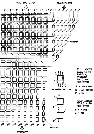
by mxn AND gates. The design of an 8x8-bit unsigned array
»
w
e
2 «
?
u 01
*—4
0! (Si j. L L <0 U
(S
s-o
c
0-ft
•0
N
c
<0
01 L Q L
Ol
01 T3
f S
multiplication architecture using carry-save adders. The
advantage of this approach is that design issues are minimal
and layout is highly modular. The logic diagram of an 8x8—
bit parallel multiplier is shown in Fig. 2.12 [6]. The
implementation of such a multiplier of size nxn-bits
requires (n— 1 ) (n— 1)— 1 Full adders, n Half adders, and nxn
AND gates. Therefore the entire multiplier is designed using
three unit cells: a full adder, a half adder, and an AND
gate cell. The last stage of the array multiplier is an
(n-l)-bit ri pple- ca rry adder which can be replaced by a
carry lookahead adder to improve the speed of the operation.
2.5 PIP ELINED ARITHME TI C
2.5.1 THE CO NCE PT OF PIPELINE SYSTEM
The computing power of a machine is determined by two major
factors, one is throughput rate (bandwidth) and the other is
latency C4]. Throughput is the rate at which new data can be
fed to the processor. Latency is the time required for the
data to traverse the processor. For a system that performs
one operation at a time (such as the adders that have been
discussed so far), throughput rate is the inverse of
1 a t e n c y .
In most digital signal processing applications the
throughput rate of the processor is the critical factor, not
the latency time. In conventional designs, an increase in
the throughput rate of arithmetic processors has been
achieved by reducing the latency with faster logic
•7
"1 *S
6
*b *•5
•3 *3
*3
» T * 8 * 3 H * 3 * 0 * 1 * 0 * 7 * 1 * t * l l H * l | * « * l l * J * j * 3 * 1 1 * 1 ^ 1 * ® V |
p
3 FÎË1
fS ri3
fQ
f3
f3
It I» It It It It
rr^j
* 3 * «
JLi i i
Ï
TTTli
*0
*0*0
f,5 ',3 Nl ',q N N ^ U S « '3 *2 'o
to reduce the propagation delay time.
A simple solution to the throughput rate problem is to allow
sim ul taneous execution of many tasks by multiple arithmetic
units. Parallel pr ocessing with straight har dware
duplication, however, may not be economical or cost
effective. Pipelining allows a significant increase in
throughput rate with only moderate increase in hardware.
Pip el ine computing refers to the subdivisions of the total
computational workload into individual tasks, so that they
can be executed in an ov erlapped fashion through a h i g h
speed arithmetic pip e l in e under certain pr ece d en c e
constraints. The functional organization of a pipelined
arithmetic unit is illustrated in Fig. 2.13 . The pi pe li ne
is characterized by the success io n of stages. In a pipelined
structure, s uc ces si ve stages are interfaced with data
latches ( synchronized regis te rs ), which hold the input and
output bit pattern of the successive stages. Dif ferent
stages may have different delay times. In order to re gu lat e
the pip eline operation, the synchronizing clock pulse should
ha v e a clock period of
T > Max { Ti + T1 } i ^ Cl , k]
Wh er e Ti is the d ela y time of the i-th stage and Tl is the
delay time of a sin gle latch. Therefore the th roughput rate
of the pipelined syst em is determined by the ma x im u m de la y
of one stage plus the d ela y time of a latch. The latency of
N P U I S
STAGE 1
STAGE 2
STAGE N
CLOCK
L A K H
L A K H
L A K H
2 .5.2 PI PELINED CARRY-SAVE ADDER (HALF ADDER ARRAY)
Pip elined adders remove the proble m of carry propagation at
the cost of extra hardware. Fig. 2.14 shows the
ar ch itecture of a fully pipelined adder using an array of
half adders. The pipelining is achieved by placing latches
between each stage of operation. In this way the inputs can
arrive separated by only one clock cycle. The maximum clock
freq ue ncy of operation is determined by the delay of a half
adder plus the delay of a single latch.
2 .5.3 PI PELINED RI PP LE-CARRY ADDER (FULL ADDER ARRAY)
The general architecture of a pipelined rip p le —carry adder
(FA array) is shown in Fig. 2.15. This design requires less
ha rd war e than the similar stru ct ure using an array of half
adders (almost 25% reduction in transistor count). As
before, throughput rate of this structure is determined by
the delay time of a full adder plus the delay of a latch.
A 10— bit pipelined ripple—car ry adder was implemented using
3um CMOS technology. Appendix B (Fig. B-5) shows the chip
layout of this adder.
2 . 5 . 4 PIP ELI NE D CARRY L O O KA H EA D ADDER
In section 2.3.3, the or g ani za tio n of the first order
(two-level) carry lookahead adder was discussed. This adder can
be converted to pipelined version by placing latches between
the different stages. Figure 2.16 shows the architecture of
a 16-bit pipelined carry lookahead adder. The adder has five
M
O
iBi]
«1
m e
i
M
S6
S5
S4
S3
S2
SI
so
s e
M W
fi B3
c B2
Al 81
I
55
S5
SA
S3
S2
SI
SO
B
j
16C . ,
1
• 'C*»i
c*
16 16
16
First order P/G Unit
First order CLA Unit
Carry Prooagate/Generate Unit
Carry Look—Ahead Unit
Sum Unit
CARRY OUT S U M
stage 1 - Propagate / Generat e Unit:
Each pair of input bits < A, B) is used to produc e the
ge nerate (G) and prop aga te (P) bits according to the
following equations
P = A © B
G = A . B
Stage 2 — First Order Pr opagate / Generate Unit:
Each group of four gen er ate and propagate signals from the
previous stage are used to produ ce the first order propagate
and generate vectors according to the following equations:
I
PO = PO PI P2 P3 I
GO = G3 + G2 P3 + GI P2 P3 + GO PI P2 P3
I
PI = P4 P5 P6 P7
I
GI = G7 + G6 P7 + G5 P6 P7 + G4 P5 P6 P7 1
P2 = PS P9 PIO Pll
\
G2 = Gll + GIO Pll + G9 PIO Pll + G8 P9 PIO Pll
P3 = P12 P13 P14 P15 \
G3 = G15 + G14 PIS + G13 P14 PIS + G12 P13 P14 PIS
Stage 3 — First order Carry Lookahead Unit:
First order propagate / gen e ra t e vectors are used with the
carry input Cin to produc e the intermodular carry signals
according to the following equ ations :
\ I
C3 = GO + Cin PO
' V < \ %
C7 = GI + GO PI + Cin PO PI
\ \ \ ' \ \ ^ t \
Cll = G2 + GI P2 + GO PI P2 + Cin PO PI P2
\ I I I I I I
CIS = G3 + G2 P3 + GI P2 P3 + GO PI P2 P3 + Cin PO PI P2 P3
St ag e 4 — Carry Lo okahead Unit :
according to the -following equations
CO = GO + Cin PO
Cl = GI + GO PI + Cin PO PI
C2 = G2 + GI P2 + GO PI P2 + Cin PO PI P2
C4 = G4 + C3 P4
C5 = G5 + 64 P5 + C3 P4 P5
C6 = 66 + G5 P6 + G4 P5 P6 + C3 P4 P5 P6
C8 = G8 + C7 P8
C9 = G9 + GS P9 + C7 P8 P9
CIO = GIO + G9 PIO + G8 P9 PIO + C7 PS P9 PIO
C12 = G12 + Cll P12
C13 = G13 + G12 P13 + Cll P12 P13
C14 = G14 + G13 P14 + G12 P13 P14 + Cll P12 P13 P14
Stage 5 - Sum Unit
In the sum unit, the carries are combined with the generate
signals to produce the sum bits
Si = Pi © Ci-1
As before, pipelined registers are used between the stages.
The pipelined carry lookahead adder has the advantage of
smaller latency time compared to the pipelined ripple carry
a d d e r . For a 16-bit pipelined ri pple-carry a d d e r , 16 clock
cycles are required befo re the first result is output while
the pipelined carry lookahead adder req uires only 5 clock
cycles. The d i s a d va nt a ge of the pipelined carry lookahead
adder is its irregular structure compared to the pipelined
rip pl e -carry adder ( HA & FA a r r a y ) . The throughput rates
2 . 5 . 5 PI P ELI NE D MULTIP LI ER
Most digital signal processing algorithms require the use of
high-s pe ed multipliers. In app lications where a multiplier
is operating on a input data stream, a pipelined multiplier
is used to improve the throughput rate of the operations.
The maximum clock rate of a pipelined multiplier is
determ in ed by the delay due to one stage, which is equal to
the delay of a full adder plus a register. F i g . 2.17 shows
the schematic block diagram of a multiplier array using a
c a r r y —save adder (CSA) te chnique C3I. It is readily observed
that data flows verti cal ly from one stage to the next. The
registers, which are placed at the outputs of each
individual cells, make the ar ch it e ct u re fully pipelined.
This method results in a hi gh- throughput rate operation.
Further improvement in speed is still possible by replacing
each full adder by two hal f -a d de r s and then pipelining the
half adders. In this way the throughput rate is determined
by the ha l f — adder delay plus a register. Since the chip area
will increase co n sid er ab ly the ar ea-time product of this
MJ_TIPLICAhO MULTIPLIER
2' 2* 2* 2* 2* 2* 2‘ 2* 2* 2' 2* 2* 2“ 2* 2* 2'
t I t I f f t J_ I t I I I I I
rii ni ni Pi Pti Pti
Pii □□□□□□
I II ) I
msnx
!J L _ D
ruLL AOOER CELL WITH PARTIAL PRODUCT SATE AM) % Z I S T E R
s - Ae ee o
*m. ^autim. mouCTi Q ■ aS*AO *SO
P • XT
h a l t ADDER CELLS WITH REGISTER
S • A « B C • AS
D D
«
. I
I
T
j
i
I
2“ 2" 2'* 2‘* 2" 2" 2' 2*
PRODUCT.
mSTCR
C H APT ER 3
RESI DU E ARITHMETIC AND DE S I G N OF HIG H- SP E ED RNS ADDER
3.1 INTRODUCTION
This chapter des cribes the r e p r é s e n t â t ! on of a number in the
Residue Number System (RNS), and will also discuss the
operat io ns of addition, subtraction, and multiplication
using the RNS representation. VLSI implementations of RNS
adders are discussed and four different realisation
approaches are presented: Binary a d d e r , look— up table,
hybrid, and counter— based m e t h o d . In the final part of this
chapter a pipelined Binary ri ppl e- ca r ry adder is compared
with a pipelined RNS adder (r i p p 1e - c a r r y - b a s e d ) and the
a d van ta ges of the RNS adder over the Binary adder are shown.
3.2 RE S ID U E R E P R E SE N TA T IO N
The Residue Number Sys tem is a nonweig hte d integer number
system which is described by an N-tupl e of integers [7] :
1 2 3 N
called moduli (each number is called a modulus). The
rep re sen ta tio n of an integer X in RNS takes the form of an
N-tupl e of residues,
X ““ { X , X , X . . . ...,x }
1 2 3 N
Where x is the remai nd er of X when divide d by m . The
i i
following set of N eq u a ti o ns d ef i n e x i
X = q m + X i = 1 , 2 , 3 ... N
By de-finition x must be pos itive and less than m . So qi
is the integer value of the quotient X/mi which is denoted
by [X/mi]. The quantity xi is designated as residue of X
mo du l o mi (also known as X mod mi) or ! X I mi . Therefore we
can write
X = mi [ X / m i ] + xi
The dynamic range of X is represented by
O < X < M
M = ml.m 2 ... mN
The residue representation of a number is unique but the
co nv e r se of the statement is true only if :
(1) The set of moduli are pai rwi se rel ative prime
(2) Only numbers within the dynamic range are considered
Example 1
Co nsider a Residue Number Syst em with moduli ml = 3 and m2 =
5. What is the residue r e p r é s e n t â t ion of X = 13 ?
For ml = 3 we obtain C 13/3] = 4 and for modulus 5 the
integer value is C13/5] = 2 . Hence
xl = X - ml CX/ml] = 1 3 - 3 * 4 = 1
x2 = X - m2 CX/m2] = 1 3 - 5 * 2 = 3
T h e r ef or e the residue r e p r é s e n t â t ion of 15 is { 1 , 3 }
Table 3.1 shows the residue repr es ent at io n of the numbers —4
to 20 for moduli 3 , 5 .
Ex am ina ti on of table 3.1 shows that residue rep resentation
is periodic (in this case the period is 15). If the Re sid ue
Number System is restricted to a single period, ambiguity in
![Fig. 2.5 [4]. The additional input P is used](https://thumb-us.123doks.com/thumbv2/123dok_us/1461752.1179111/24.632.75.554.61.743/fig-additional-input-p-used.webp)