ISSN(Online): 2320-9801
ISSN (Print): 2320-9798
I
nternational
J
ournal of
I
nnovative
R
esearch in
C
omputer
and
C
ommunication
E
ngineering
(An ISO 3297: 2007 Certified Organization)
Vol. 3, Issue 2, February 2015
Design of SRAM Cell by Using Self-
Controllable Voltage Level Circuits
Akshaya.N
1, Bini Joy
2, Sathia Priya.M
3, Arul Kumar.M
4PG Students, Dept of ECE, SNS College of Technology, Coimbatore, India1,2,3,4
ABSTRACT: Memory is the most common part in CMOS applications. The power consumption and speed are important issue that has led to multiple designs with the purpose of minimizing the power during both read and write operations of SRAM .In modern high performance integrated circuits more than 40% of the total active mode energy is consumed due to leakage currents. The feature size of the transistor is scaled down the threshold voltages of MOSFETs have been reduced thereby increasing leakage power substantially. Leakage is the only source of energy consumption in an idle circuit .SRAM arrays are important sources of leakage since the majority of transistors are utilized for on-chip memory in today‟s high performance microprocessors and systems-on-on-chips. A new leakage current reduction circuit called improved Self-controllable Voltage Level (SVL) circuit is developed and included to reduce the leakage power of 6T SRAM. Simulation result of 6T SRAM with improved SVL design using TANNER tool shows the reduction in total average power and delay.
KEYWORDS: Leakage power, MOSFET, SRAM, SVL
I. INTRODUCTION
Random access memory is a type of memory that provides the direct access to any byte on the chip and byte addressing means the contents of any byte can be read or written without regard to the bytes before or after the read and write speeds. RAM plays an important role in many systems such as computer and communication systems; and there is several applications software used for implementing the digital circuits of RAM. It takes no longer to write a byte than it does to read one. RAM (also referred to as read-write memory) is considered volatile storage because its contents are lost when the power is removed. Computer and other types of system require the permanent or semi permanent storage for large amounts of binary data. Memory is the portion of a system used for storing binary data in large quantities.
Memory unit is a device to which binary information is transferred for storage and from which information is available when needed for processing. Binary information received from the input device is stored in memory and information transferred to an output device is taken from memory. There are two categories of memory in current use; semiconductor and magnetic within each category are a variety of memory types, generally the semiconductor memories are used for smaller capacity and faster access applications.
Normally RAM consists of the following connections:
Address lines means it defines the memory location to be selected for read or write.
Input/output data lines mean it defines the data to be written or read from memory.
Write enable (WE) is a control input that selects between the memory read and write operations (usually active low).
Output enable (OE) is a control input that enables the output buffer for reading data from the memory (usually
active low).
Chip select (CS) selects the memory (usually active low).
ISSN(Online): 2320-9801
ISSN (Print): 2320-9798
I
nternational
J
ournal of
I
nnovative
R
esearch in
C
omputer
and
C
ommunication
E
ngineering
(An ISO 3297: 2007 Certified Organization)
Vol. 3, Issue 2, February 2015
II. EXISTING METHOD
A. 9T SRAM
SRAM consists of a simple latch circuit with two stable operating points. SRAM requires nine transistors per bit also. A new nine transistor (9T) SRAM cell with reduced leakage power consumption and enhanced data stability is proposed in this paper. 9T SRAM is implemented to reduce the power consumption of the SRAM cell and the bit line leakage. The leakage power consumption of the new SRAM cell is reduced by 99.99% as compared to the conventional nine-transistor (9T) SRAM cells. The 9T SRAM cells consist of two data access mechanisms for the read and write operations. During a read operation, the storage nodes are completely isolated from the bit lines. The 9T memory cell has nine transistor (N1, N2, N3, N4, N5, N6, N7, P1, P2) with minimum sized device been implemented with two cascade dynamic inverters (P1, N1, N2, P3, N4 and N3) which operate at different clock rates. The voltage drop at the read bit line due to the leakage current is still sufficiently small to retain correctness in the data.
B. Read operation
During read operation both BL and BLB is made high. To read logic „0‟ node A is grounded so that the transistors P1and P2 will be in ON state there by the voltage is discharge through access transistor N3 via P1 and P2. During this time node BL is high which makes transistor N1 and N2 ON there by charges the access transistor N4 given in figure 3.1. The sense amplifier detects the logical levels of BL and BLB. If BL is discharge then the data read is „0‟.Similarly to read logic „1‟ node BL is grounded so that the transistors N1 and N2 in ON state there by the voltage is discharged through the access transistor N4 via N1 and N2. Performance is an important issue in SRAM design due to ever increasing demand for these modules.
Pull down ratio (PD) = 𝛽𝑁
𝛽𝐴 --- equ (2)
βN = transconductance of pull down NMOS (N1 and N2)
βA = transconductance of access transistor (N5)
Figure 1 9T SRAM Cell
ISSN(Online): 2320-9801
ISSN (Print): 2320-9798
I
nternational
J
ournal of
I
nnovative
R
esearch in
C
omputer
and
C
ommunication
E
ngineering
(An ISO 3297: 2007 Certified Organization)
Vol. 3, Issue 2, February 2015
C. Write Operation
During write operation BL and BLB should be complementary to each other. To write logic „0‟ the preliminary condition has to check. If previously stored value is „1‟ the status of node BL is high and node BLB is Low. Therefore to write logic „0‟ force node B to high thereby the node voltage at BL will be discharged through P1 and P2. Similarly to write logic „1‟check the previously stored values of node B and BL. If previously stored value is „0‟ the status of node BL is low and node BL is high. Therefore to write logic „1‟ force node BL to high thereby the node voltage at BL will be discharged through BLB. For write stability the aspect ratio of the transistors N1 should be lesser than N4.
The aspect ratio of pull up network of transistor βP (N1) to access transistor βA (N4) is called pull up ratio .
Pull up ratio (PU) = 𝛽𝑃
𝛽𝐴 --- equ (2)
βp = transconductance of pull up PMOS (P3)
βA = transconductance of access transistor (N6)
This parameter PU defines the write stability of the SRAM cell. In this proposed 9T SRAM the transconductance ratio of (βP/βA<1) is made lesser than 1.
III. PROPOSED METHOD
A. Self-Controllable Voltage Level
A self-controllable voltage level (SVL) circuit which can supply a maximum dc voltage to an active-load circuit on request or can decrease the dc voltage supplied to a active-load circuit in standby mode was developed. This SVL circuit can drastically reduce standby leakage power of CMOS logic circuits with minimal overheads in terms of chip area and speed. SVL can also be applied to memories and registers because such circuits can retain data even in the standby mode. There are two well-known techniques that reduce leakage power (Pst). One is to use a
multi-threshold-voltage CMOS (MTCMOS) . It effectively reduces Pst by disconnecting the power supply through the use of
high Vt MOSFET switches. The serious drawbacks such as the both memories and flip-flops cannot retain data. The
other technique involves by using a variable threshold-voltage CMOS (VTCMOS) this reduces Pst by increasing the
substrate-biases and it also faces some serious problems, such as a large area penalty and a large power penalty due to the substrate-bias supply circuits requires low leakage power. The basic idea is that when the SRAM cell is in active mode means, the CL is low. And there is no degradation in noise margin. During standby mode, CL is high and reduced
supply voltage is given to SRAM cell. This reduces the leakage current and also reduces noise margin.
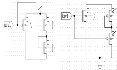
B. Improved Self-Controllable Voltage Level Circuits
3.2.1 Upper SVL Circuit
In Upper SVL circuit the impedance of a MOS transistor increases with the width of the transistor.PMOS1
having width means it offers very high resistance in that path between Vdd and Vd . The NMOS1 and NMOS2 form a
read and write working in normal mode of the cell. NMOS2 acts as a resister to reduce current in active mode by connecting upper SVL circuit so that leakage power is reduced.
3.2.2 Lower SVL Circuit
In lower SVL circuit the impedance of a MOS transistor increases with the width of the transistor. NMOS3
having width means it offers very high resistance in that path between vdd and vd. NMOS3 work in the SVL mode and
PMOS2 and PMOS3 work in the normal mode of the cell. PMOS2 acts as a resister to reduce leakage power. The lower SVL circuit which incorporates a single n-SW and m p-SW connected in series is given in the figure 3 is located
ISSN(Online): 2320-9801
ISSN (Print): 2320-9798
I
nternational
J
ournal of
I
nnovative
R
esearch in
C
omputer
and
C
ommunication
E
ngineering
(An ISO 3297: 2007 Certified Organization)
Vol. 3, Issue 2, February 2015
Figure 2 Upper SVL Circuit And Lower SVL Circuit
These two techniques reduce leakage current. The role of SVL circuits is to reduce leakage currents in standby mode or hold mode because so much leakage power in stand by mode can destroy the cell .When the inputs logic 1 and 0 to the SVL circuits we can say that the cell operates in hold mode. In this mode NMOS8 on the upper SVL circuit and PMOS4 on the lower SVL circuits are compared to reduce the leakage. NMOS9 and PMOS3 and also to reduce leakage power. In other modes the cell operates as normal operations read and write. In write mode SVL provides expansion of the noise margin.
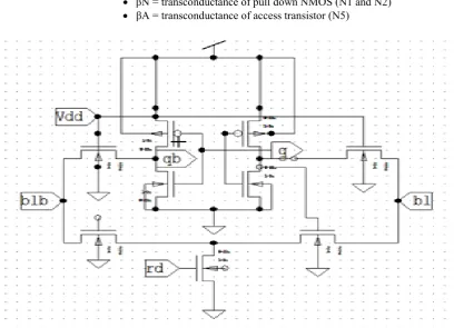
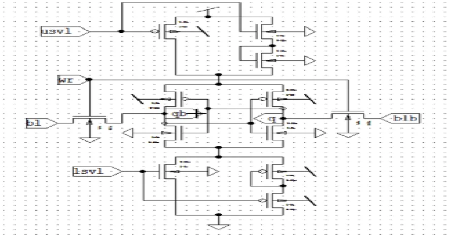
C. 9T SRAM SVL
ISSN(Online): 2320-9801
ISSN (Print): 2320-9798
I
nternational
J
ournal of
I
nnovative
R
esearch in
C
omputer
and
C
ommunication
E
ngineering
(An ISO 3297: 2007 Certified Organization)
Vol. 3, Issue 2, February 2015
Figure 4. 9T SRAM with improved SVL
D. 6T SRAM with SVL
6T SRAM consists of a simple latch circuit with two stable operating points. SRAM requires six transistors per bit also called full SRAM cell(P1 P2 N1 N2 N3 N4) .If the memory cell is selected by raising the voltage of the word line to "1" pass transistors N3 and N4 are turned on is shown in the figure 5 once the SRAM cell is selected a read or write can be performed.
ISSN(Online): 2320-9801
ISSN (Print): 2320-9798
I
nternational
J
ournal of
I
nnovative
R
esearch in
C
omputer
and
C
ommunication
E
ngineering
(An ISO 3297: 2007 Certified Organization)
Vol. 3, Issue 2, February 2015
To store a logic "1" to the cell bit line (BL) is forced to logic "0" by a the data write circuit. this action turns driver transistors M3 off and transistor M4 on forcing Q to logic "1". When logic "1" is stored in cell and the in order to read its valve the voltage of column (BLB) is slightly pulled down by transistors P1 an N3. This small voltage difference at bit line is sensed by the data read circuit and amplified as a logic "1" to the output. During read the WL voltage is raised, and the memory cell discharges either BL (bit line) or BLB (bit line complement) Depending on the stored data then at the end of the read cycle, the BLs supply returns to the positive supply rail. During write mode WL is raised and the BLs are forced to either power supply (depending on the data) . During hold state , WL is held low and the BLs are left floating or driven to VDD. When a conventional SRAM cell is in the read operation, the pass gate is turned on and pulls the node that stores the logic “0” to a non-zero value. This decreases the read SNM ratio, especially when a low power supply voltage is utilized and the read SNM ratio is very low.
IV. SIMULATION RESULTS
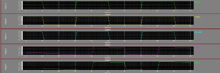
Simulation results are performed using Tanner EDA tool in 125nm technology with supply voltage ranging from 5v and operating frequency of 50MHZ. To establish an impartial testing environment each circuit have been tested on the same input patterns. The below waveform shows proposed 9T SRAM with SVL for the inputs wr , rd and bl and respective outputs are q and qb
Figure 6 Output Waveform of 9T SRAM with SVL
The below waveform shows proposed 6T SRAM read for the input rd bl and blb and respective outputs are q and qb.
ISSN(Online): 2320-9801
ISSN (Print): 2320-9798
I
nternational
J
ournal of
I
nnovative
R
esearch in
C
omputer
and
C
ommunication
E
ngineering
(An ISO 3297: 2007 Certified Organization)
Vol. 3, Issue 2, February 2015
A. PERFORMANCE ANALYSIS
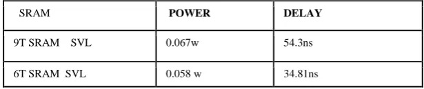
Comparison table depicts the transistors over a range of Power Supply. It is shown that the proposed technique has minimum Power and transistor count.
Table 2 COMPARISON TABLE FOR 9T SRAM AND 6T SRAM
V. CONCLUSION
The effect of the improved SVL circuit describing the leakage current through the load circuit was implemented. The improved SVL circuit and the load circuit were designed by using tanner technology. Sub-threshold memory design has received a lot of attention in past few years but most of them use large number of transistors to achieve sub threshold region operation. The advantages of different modes i.e its operating mode is high Vds to load
circuits and for high speed operation in stand-by mode, high Vt through load circuits for minimum stand-by leakage
power, high noise immuntiy, stand-by power dissipation and delay. In future it is possible to implement SVL method in DRAM because of low cost and reduction in number of transistors.
REFERENCES
1] Y.Chung, D.Y. Lee “Differential-read symmetrical 8T SRAM bit-cell with enhanced data stability” ELECTRONICS LETTERS Vol.46 No. 18 2nd Sep. 2013
2] L.Chang, et al, “An 8T-SRAM for Variability Tolerance and Low-Voltage Operation in High-Performance Caches” IEEE journal of solid-state circuits, VOL. 43, NO. 4, April 2013
3] V.Gupta and M.Anis, “Statistical Design of the 6T SRAM Bit Cell” IEEE Transactions on Circuits and Systems VOL. 57, NO. 1, January 2012. 4] Z. Liu and V.Kursun “Characterization of a Novel Nine-Transistor SRAM Cell” IEEE Transactions on Very Large Scale Integration(VLSI) Systems, Vol. 16, no. 4, April 2012.
5] S. Kaur, A. Kumar “Analysis of Low Power SRAM Memory Cell using Tanner Tool” IJECT Vol. 3, Issue 1, Jan. - March 2012. 6] Martin Mangla, “Low Power SRAM Circuit Design”, Department of electrical and computer engineering, University of Alberta,2013 IEEE. 7] Shyam Akashe, Meenakshi Mishra,and Sanjay Sharma,"Self controllable voltage level circuit for low power, high speed 7TSRAM cell at 45nm technology", 2012 IEEE Trans
8]Sheng Lin , Yong Bin Kim , Fabrizio Lombardi “A Low Leakage 9T SRAM Cell for Ultra-Low Power Operation” ACM GLSVLSI‟08, May 4–6, 2013
9] Tadayoshi Enomoto, Yoshinori Oka "A Self-Controllable-Voltage-Level (SVL) Circuit for Low-Power, High-Speed CMOS Circuit"
10]R.Venkatraman et al., "The design, analysis, and development of highly manufacturable 6T SRAM bitcells for SoC applications,"IEEE Trans. Electron Devices, vol. 52, no. 2, pp. 218–226.
SRAM POWER DELAY
9T SRAM SVL 0.067w 54.3ns