ECE250 Electronics and Device Modeling Laboratory Project #5
BJT Digital Logic Gate Circuits (KEH)
Dept. of Electrical and Computer Engineering, Rose-Hulman Institute of Technology Lab Team Members:_____________________ ______________________ Date Performed: ________________ Lab Station #_______
Parts Required:
4x 2N2222 NPN Bipolar Junction Transistors (BJTs) 2x 47kΩ resistors
3x 1kΩ resistors 2x 10kΩ resistors 3x 100Ω resistors 1x 0.1μF capacitor
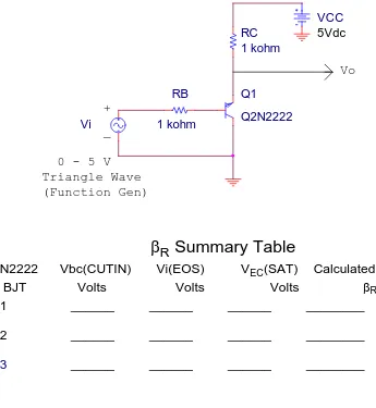
Part 1, BJT Inverter VTC and βF measurement. Obtain four 2N2222 BJTs and line them up on your lab table, so that all four of the BJTs can be distinguished later. Think of the leftmost BJT as BJT #1, etc. Now connect BJT #1 as a saturating inverter, using the circuit shown in Fig. 1. Let the dc power supply voltage (Vcc = +5 V) be your dc 0 - 6 V bench power supply. Let Vin be your function generator, which will be set up to deliver a 0 - 5 V triangle wave, following the procedure outlined in the steps listed below.
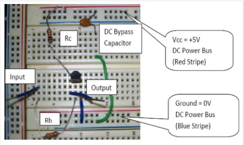
Note: In this circuit, and in all the remaining circuits you build in this course, please use the RED horizontal trace at the top of your breadboard as the "Vcc power distribution bus" to distribute the Vcc = +5 V dc power, and the BLUE horizontal trace at the bottom of your breadboard as a "ground bus" to distribute the 0 V dc power. Also, please connect at least one 0.1 μF capacitor
between the Vcc and ground bus to "locally bypass to ground" any ac noise created by a device that is connected to the dc power bus. Often, several 0.1 μF "bypass" capacitors are used, where each capacitor is placed as close to the +5 V and 0 V (ground) power pins of each device that is likely to cause such noise.
2N2222A and 2N2222 (plastic case) NPN BJT - (Flat Surface Toward You!)
C C B E C E E
[image:1.612.82.285.593.720.2]2 N39 04 B B C 2N2222A B E 2N2222
Fig. 1a. BJT Common-Emitter Saturating Inverter Schematic
Fig. 1b. BJT Common-Emitter Saturating Inverter Breadboard Layout.
Note the use of the Vcc dc power distribution bus (Red Stripe at top), the 0 V DC Ground bus (Blue Stripe at bottom), the DC Power Bus AC (Noise) Bypass capacitor. The BJT does NOT have its leads bent, but it plugged
"Vo vs. Vi" Voltage Transfer Curve Using the Agilent 33120A & 33220A Function Generators
0. Before beginning this or any lab experiment, please make sure each of the oscilloscope probe inputs on the oscilloscope have been configured for 10:1. See me if you need help doing this!
1(a) Agilent 33120A 15 MHz Function Generator: Press purple SHIFT key and then press the ENTER (MENU) key. Press ">" right arrow key three times to scroll to "D: SYS MENU". Press down arrow key "v" once to get to "1: OUT TERM". Press down arrow key again "v" and then press ">" right arrow key until "HIGH Z" mode is selected. Finally press ENTER key.This calibrates the output of the function generator assuming a high impedance load. If you allow the default setup condition (50 OHM) to prevail, then the unloaded generator output voltage will be twice what you set it for, since the default assumes the generator (which has an internal 50 ohm output impedance) is working into a 50 ohm load, and thus the generator must develop an internal Thevenin equivalent voltage that is twice the specified terminal value!
(1b) Agilent 33220A Function Generator: Hit the Utility button on the function generator, then press the Output Setup soft key. Then select High Z. This calibrates the output of the function generator assuming a high impedance load. If you allow the default setup condition to prevail, then the unloaded generator output voltage will be twice what you set it for, since the default assumes the generator (which has an internal 50 ohm output impedance) is working into a 50 ohm load, and thus the generator must develop an internal Thevenin equivalent voltage that is twice the specified terminal value! Hit the Utility button once again to exit from this menu.
2(a) Agilent 33120A 15 MHz Function Generator: Press FSK Button (3). This generates the triangle wave. Now press the Freq button and set to 100 Hz, Press Ampl button and set to 5.0 Vpp, Press Offset button and set to 2.5 V. A 100 Hz triangle wave that varies from 0 V to 5 V should result (check this on the scope)
(2b) Agilent 33220A Function Generator: Select the "ramp" waveshape by hitting the Ramp button, and set Freq = 100 Hz, Amp = 5.0 Vpp, Offset = 2.5 Vdc, and Symmetry = 50%. You can hit the Graph button to see your waveform setup. Hit the Output button to start the generator.
(3) Now connect the function generator output in place of the dc source labeled "Vi" in Fig. 1 Connect CH1 (X input) of the Agilent 54624A or 54622D oscilloscope (using the scope probe provided) across the function generator. Display this waveform vs. time (using the Autoscale button), and make final adjustments to the function generator Amplitude and DC Offset in order to ensure that the function generator is delivering a triangle wave that varies precisely between 0 V and 5.0 V.
(4) Connect the CH2 (Y input) of the oscilloscope (using the scope probe provided) between the Vo terminal and ground. Verify that this second trace is switching the BJT between saturation (0.2 V or so) and cutoff (5.0 V) levels.).
(5) Now put the scope in "X-Y" mode, which allows us to plot one voltage vs. another. Do this by hitting the "Main-Delayed" button at the top left of the oscilloscope panel, and then hit the XY softkey that appears. The Vo vs. Vi voltage transfer curve (VTC) should now appear on the oscilloscope display!
(6) Adjust the "5v - 1mv" channel sensitivity knobs located above the lit Channel 1 and Channel 2 indicator buttons to display convenient sensitivities, such as 200 mV/div on CH1 (X) and 1 V/div on CH2 (Y).
(7) Now adjust the X and Y position knobs (located just above each of the scope probe connectors on the oscilloscope front panel) to adjust the 0V horizontal and vertical reference position markers to the lower left of the screen, centered on a convenient pair of horizontal and vertical graticule lines. (Note that the 0V reference positions are indicated by ground arrow symbols along the top and left screen borders.)
(8) Press the Cursors button on the scope in order to allow points on the VTC to be recorded accurately. Notice that the X and Y softkeys can select whether the cursor position reads horizontally or vertically.
In your "mind's eye", extend straight lines through the straight parts of this screen shot in order to estimate the value of Vbe(CUTIN), which corresponds to the value of input voltage Vi at which the output voltage Vo begins to move downward from its Vcc value. Also estimate the value of input voltage Vi at which the output voltage Vo stops descending and levels off (saturates). Let us call this value Vi(EOS), which denotes the value of the input voltage Vi at the "edge of saturation". Also record the observed value of Vce(SAT), which is the value of output voltage Vo that is reached at the edge of saturation. Note that Vo is approximately held at this value as Vi increases past Vi(EOS).
While the BJT is in its active region (where Vo is linearly descending) recall that Vo is given by
Vo Vcc βF Vi−Vbe CUTIN( ) Rb
⎛⎜
⎝
⎞⎟
⎠
⋅ ⋅Rc
−
=
You may replace Vo with Vce(SAT) and Vi with Vi(EOS) to solve for the βF of the BJT.
Include the screen-captured VTC, along with your βF calculations, as Attachment A. Repeat the above measurements and the βF calculation for BJT #2 and BJT #3, however in order to save paper, do not bother to print out the screen shots for these other two transistors; instead, simply read the necessary values from the oscilloscope display. Then fill in your results for these three BJTs in the "βF Summary Table" below. The 2N2222 BJT is specified to have a βF range anywhere between 50 and 250, so don't be surprised if your βF values vary somewhat from one BJT to the next.
β
FSummary Table
2N2222 Vbe(CUTIN) Vi(EOS) VCE(SAT) Calculated. BJT Volts Volts Volts βF
#1 ______ ______ ______ ______
, #2 ______ ______ ______ ______
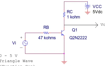
Part 2. βR Measurement. Now build the inverter circuit of Fig. 2, where the emitter and collector have been interchanged, and the base resistor has been reduced to RB = 1 kΩ,
since the BJT operated in reverse-active mode will have a value of βR that is much less than
βF. Once again, obtain a screen shot of the VTC for the first BJT, and from this, measure
VBC(CUTIN), Vi(EOS), and VEC(SAT). (You may have to increase the maximum value of Vi
above 5 V if Vi(EOS) is not reached when Vi = 5 V.) Finally, calculate βR for each of the three
[image:5.612.91.436.238.613.2]BJTs. Include the screen shot and the calculations for only one of the BJTs in Attachment B, and enter your results for all three BJTs into the "βR Summary Table" below.
Fig. 2. BJT Saturating Inverter using BJT in Reverse-Active Mode
Q1
Q2N2222
_ +
(Function Gen)
RC 1 kohm
Vo
RB
1 kohm
0 - 5 V Triangle Wave
Vi
VCC
5Vdc
β
RSummary Table
2N2222 Vbc(CUTIN) Vi(EOS) VEC(SAT) Calculated.
BJT Volts Volts Volts βR
#1 ______ ______ ______ ________
#2 ______ ______ ______ ________
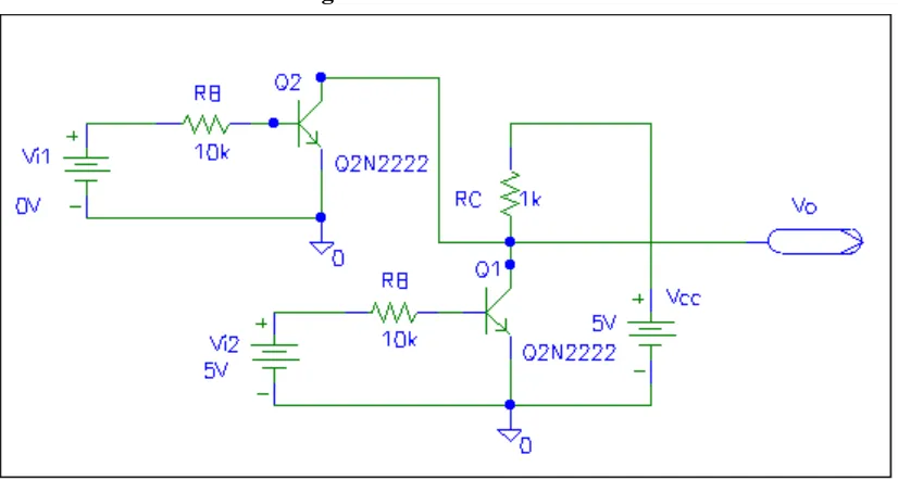
Part 3. RTL NOR Gate and SR Latch. Imagine that two of the BJT inverter circuits like that shown in Fig. 1 have had their outputs tied together (this is called "wire ANDing"). This results in the NOR logic gate circuit of Fig. 3. (The two collector resistors are now in parallel, so they have been replaced by just one pull-up resistor.) The BJT inverter outputs may be tied together without causing output line "contention" (dispute over what logic level is to be established at the output node when one inverter's output is driven HIGH and the other inverter's output is driven LOW) because this saturating inverter circuit has a strong pull-down (a saturated BJT has a relatively low collector-to-emitter resistance, on the order of perhaps 3 ohms) and a weak (1 kΩ) pull-up. Therefore if both inputs are pulled LOW, so each BJT is cut off, the output node will be pulled high, due to the "weak pull-up" action of the RC = 1 kΩ collector resistor.
However, if one or more of the inputs are raised HIGH, then one or more of the BJTs will
saturate, thereby pulling the output node down to logic LOW level, since the saturated BJT acts like a a very low resistance, RCE(sat), (only a few ohms) in series with a Vce(SAT) = 0.1 V
source between its collector and emitter terminals. The output node is pulled down toward ground much more strongly than the 1 kΩ pull-up resistor can pull the node up toward Vcc. The situation can be viewed as a voltage divider, formed by RC (1 kΩ in this circuit) and the
saturated BJT's C-E resistance, RCE(sat), which is typically about 3 Ω. Thus
VO
(
VCC−VCE(sat))
RCE(sat)
RCE(sat)+RC
⋅ +VCE(sat)
=
VO (5−0.1)
3
3+1000
⎛⎜
⎝
⎞⎟
⎠
⋅ +0.1
:= => VO = 0.114656 V
(Very close to the desired value of 0 V!)
Because the only way to get a HIGH voltage level out is to have all inputs LOW, thereby cutting off all of the BJTs, this circuit functions as a NOR gate. By wire AND-ing together "N" BJT inverter circuits, an N-input NOR gate can be realized. This type of logic circuit was used in the RTL (resistor-transistor logic) commercial logic family that was briefly used in the1960s. This circuit forms the "front end" of the 74LS02 NOR gate that is still in use today.
(a) Build the NOR gate circuit of Figure 3 using two of the BJT #1 for Q1 and BJT #2 for Q2. Note that you do NOT need to actually connect two extra voltage sources, Vi1 and Vi2. Instead, please verify the operation of this circuit by alternately connecting the inputs (via long wires) to either the GROUND bus or the Vcc bus. Try all four possible input situations, and record the value of Vo using your DVM. Fill in the table below to verify that this circuit acts as a NOR gate (the only way to get a HIGH level out is to have both inputs LOW.
NOR Gate Verification
Vi1 Vi2 Vo (measured) Vo(desired) 0V 0V ________ 5 V0V 5V ________ 0 V
5V 0V ________ 0 V
(b) Observe the VTC of the NOR gate by making Vi1 = 0 (connecting the Vi1 input to the ground bus). Note that this action holds transistor Q2 in cut off, and therefore it is "out of the picture". Now the NOR gate circuit of Fig. 3 has become identical to the BJT inverter circuit of Fig. 1. Connect the Vi2 input to the function generator, and obtain a screenshot of the resulting VTC, which is in effect the VTC of the BJT inverter that was obtained in Part 1, except this new circuit has a different base resistor.
(c) Predict the VTC of this NOR gate using the method for predicting the VTC of a BJT inverter that was presented in class for the BJT inverter. Use the values of Vbe(CUTIN), Vce(SAT), and βF that correspond to the specific BJT associated with input Vi2 in your prediction
[image:7.612.91.504.302.523.2]calculations. Sketch your predicted VTC DIRECTLY OVER (on the same set of axes as) the VTC screenshot recorded in Part 3(b). Of course, your observed VTC should be reasonably close to your predicted VTC! Include your VTC prediction calculations and the screen shot of your observed VTC that has been overwritten with your predicted VTC as Attachment C.
Fig. 3. RTL NOR Gate
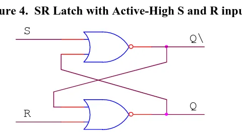
(d) Now build two RTL NOR gates, each one like the NOR gate in Fig. 3. Verify the operation of BOTH of these NOR gates, making sure that they follow the truth table recorded in Part (a) above. Then "cross-couple" them to form an SR (Set-Reset) latch with active-high S and R inputs, as shown in Figure 4. Verify that the SR latch "remembers" whether the S or the R line was last activated (raised high) by connecting long wires to the S and the R inputs. Start by grounding both wires, and observe the (random) state of "Q" on your DVM. Then momentarily raise S by connecting that wire to Vcc, and then lower it back to ground. Note that now Q must = 1, remembering it was last set. Then momentarily raise R to Vcc, and then lower it back to ground. Note that now Q must = 0, remembering it was last reset. Obtain your lab instructor's signature in the space below after you have demonstrated the proper operation of the SR latch to him. Hint: Before cross-coupling the two NOR gates, the operation (truth table) of each NOR gate should be verified separately using long wires connected alternately between Vcc and ground busses, as was done in Part 3(a).
Figure 4. SR Latch with Active-High S and R inputs
Q R
S
Q\
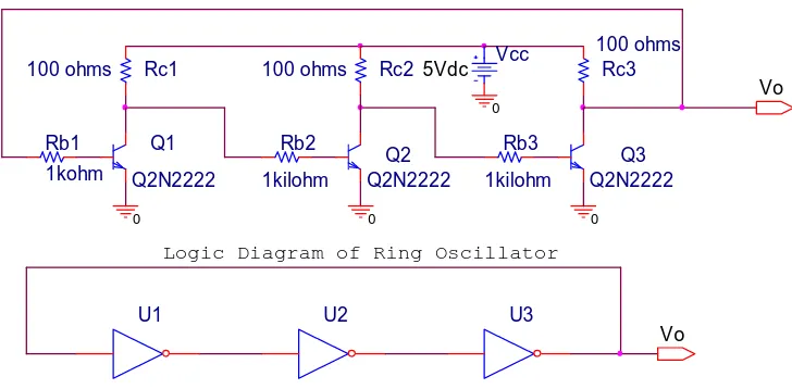
Part 4. BJT Inverter Ring Oscillator, Propagation Time, and Rise and Fall Times
If an odd number of "N" BJT inverters (where N = 3, 5, 7, etc.) are connected in a "ring" configuration, as shown in Figure 5, the circuit will oscillate, provided that the gate propagation time (Tpd) and the gate rise time (TRISE) and fall time (TFALL) meet the
following requirements:
3Tpd > TRISE and 3Tpd > TFALL
This is because if inverter U1 starts out in the high state, then one propagation time (Tpd) later the output of inverter U2 must go low; 2Tpd later the output of U3 must go high; and 3Tpd later, the output of inverter U1 must change from high to low. Similarly, 4Tpd later U2 will go high, 5Tpd later U3 will go low, and 6Tpd later U1 will change from low to high. Now the output of U1 is back where it started, and the entire cycle repeats endlessly. Note that the output Vo will be HIGH for 3Tpd and LOW for 3Tpd. The frequency of oscillation will be 1/(6Tpd).
Build the circuit of Figure 5, and obtain a screen shot of several cycles of variation of Vo(t) on the oscilloscope. Use the Agilent oscilloscope's "Quick Measure" feature to display Vo(t)'s rise time (the time the output of an inverter requires to rise from 10% to 90% of its high value), fall time(the time the output of the inverter requires to fall from 90% to 10% of its high value), and frequency of oscillation on your picture. Include this plot as Attachment D.
Note that the base and collector resistors have been lowered in order to 1kΩ and 100Ω,
respectively, to make each BJT inverter's rise and fall time faster by reducing the time required to charge the parasitic output capacitance. This was done because we desire that the output rise (o fall) all of the way before the next transition must occur (3Tpd later).
From the measured frequency of oscillation "f", calculate the average propagation delay of each inverter in the circuit below using the result derived above: f = 1/(6*Tpd), and fill the results in below. Be sure to include appropriate units.
f = ____________ Tpd = _________
Figure 5. 3-Inverter Ring Oscillator
-- Notice this circuit has no "input" terminal, as the circuit's input is taken from its output!Rb1 1kohm
Rb3
1kilohm
U2
0
U3 Rc2
100 ohms
Q2 Q2N2222
0
Rc1 100 ohms
Rb2
1kilohm
0
Q1
Q2N2222
0
U1
Vcc
5Vdc
Vo
Rc3 100 ohms
Circuit Diagram of Ring Oscillator
Q3 Q2N2222
Vo
Logic Diagram of Ring Oscillator
Debugging Hint: If the ring oscillator circuit of Fig. 3 fails to oscillate once you have built it, then break the feedback loop by disconnecting the wire connected to the output of inverter U3. (In general, systems with a feedback loop are always harder to debug than systems without feedback loops.) Now connect the free end of this wire to the Vcc bus, thereby making the input of U1 HIGH. Then use a DVM or an oscilloscope to verify that the output of U1 is LOW, the output of U2 is HIGH, and the output of U3 is LOW. If this is not true, you can check the wiring of the inverter that has failed. If all appears well, then connect the the input of U1 LOW, and now verify that the output of U1 is HIGH, the output of U2 is LOW, and the output of U3 is HIGH. Once both of these tests are satisfied, all three inverters in the loop have been checked out, and the circuit should oscillate once the feedback loop is
reconnected, assuming that each inverter's rise and fall times are fast enough compared to the inverter's propagation time so that the inverter output has finished rising or falling before the next logic change has propagated around the loop: