Organic:inorganic heterojunctions for photovoltaic
devices.
VALE, Alistair Douglas John.
Available from Sheffield Hallam University Research Archive (SHURA) at:
http://shura.shu.ac.uk/20472/
This document is the author deposited version. You are advised to consult the
publisher's version if you wish to cite from it.
Published version
VALE, Alistair Douglas John. (2005). Organic:inorganic heterojunctions for
photovoltaic devices. Doctoral, Sheffield Hallam University (United Kingdom)..
Copyright and re-use policy
See
http://shura.shu.ac.uk/information.html
CITY CAMPUS, HOWARD ST
SHEFFIELD
1VV3
ProQuest N um ber: 10701119
All rights reserved
INFORMATION TO ALL USERS
The q u a lity of this re p ro d u c tio n is d e p e n d e n t u p o n the q u a lity of the c o p y s u b m itte d .
In the unlikely e v e n t that the a u th o r did not send a c o m p le te m a n u s c rip t and there are missing p a g e s , these will be n o te d . Also, if m a te ria l had to be re m o v e d ,
a n o te will in d ic a te the d e le tio n .
uest
P roQ uest 10701119
Published by ProQuest LLC(2017). C o p y rig h t of the Dissertation is held by the A u tho r.
All rights reserved.
This work is p ro te c te d a g a in s t u n a u th o riz e d c o p y in g under Title 17, United States C o d e M icro fo rm Edition © ProQuest LLC.
ProQuest LLC.
789 East Eisenhower Parkway P.O. Box 1346
ORGANIC: INORGANIC
HETEROJUNCTIONS FOR
PHOTOVOLTAIC DEVICES
Alistair Douglas John Vale
BEng (Hons.)
A thesis submitted in partial fulfilment of the requirements of
Sheffield Hallam University
for the degree of Doctor of Philosophy
Declaration
I hereby declare that this thesis submitted for the degree o f Ph.D. is the result o f my own
research and that this thesis has not been submitted for a higher degree to any other
university or institution.
Signed
Abstract
Thin films o f Ti02 with a thickness around 200nm were produced by DC reactive sputtering at room temperature. A variety o f types o f bandgap including direct allowed, direct forbidden, indirect allowed, and indirect forbidden were observed, with good fits o f the Tauc model, between annealed and unannealed samples, and within the same sample. Planar conductivity was measured at 8.7 x 10"3Q -1 m -1, falling to 7.4 x 10~3Q -1 m _1 after annealing. Refractive index and extinction coefficient spectra were obtained via the Swanepoel technique and were found to be around 2.2 and 3 x 10"3 respectively, in the region o f weak absorption, with little change after annealing. Surface details in the micro and nano regimes showed flat films with few defects. XRD showed the Rutile phase dominating, and XPS showed correct stoichiometry. AFM showed the grain size to be in the range o f 64nm rising to 82nm after annealing. Ti02 films with an extended surface area were made using Degussa P25 and were deposited by the new technique o f flood printing developed for this research. 2D profiles o f thin films o f P25 were measured at different concentrations and the thickness o f the highly rough films was in the range o f 5/mi to 15/mi rising with increasing concentration. AFM also showed films that were highly rough in the nanoscale.
Thin films o f CuPc and Rose Bengal were deposited on differently coated substrates; F:TO, Ti02, and bare glass. The absorption spectra was seen to vary significantly with substrate, in particular, the 530nm peak o f Rose Bengal was seen to diminish greatly when the dye was deposited on Ti02 .
Heterojunction photovoltaic devices based on dye layers adsorbed on semiconducting layers were produced in fifteen different designs with each design based on another to observe the effect o f single parameters changes. Such changes included different thickness o f porous TiC>2 layer, and whether a conducting polymer layer is applied. The devices were built up on F:TO coated glass slides and electrical contacts were made by DC sputtering platinum fingers on the top. The best device design gave a fill factor o f 35.5%, and an overall conversion efficiency o f 4.2 x 10“3% . Devices were thought to be greatly affected by series resistance from the top contact being applied to a highly rough surface. The top contact on different structures were electrically characterised and were found to have resistances in the region o f kQ, which manifests as a high series resistance in the final solar cells. This is one o f the reasons for the low efficiency. The I(V) spectra o f all the devices were fitted to a diode model using an algorithm developed for this research. The model fit gave reverse saturation currents in the range o f 3.2 x 10"9 A to 7.5 x 10' 3 A. Ideality factor varied from 3.8 to 80, series resistance varied from 150 to 5000, and parallel resistance varied from 1170 to 778kO.
Acknowledgements
I would like to thank all the people who assisted me in this research. I would also like to
thank the Digital Technology Research Studentship for the funding without which the
research would have been unaffordable.
I would finally like to thank all the scientists who worked before me, without whom this
CONTENTS OF THESIS
DECLARATION ABSTRACT ACKNOWLEDGEMENTS CHAPTER 1 INTRODUCTION1.1. General Introduction 1.2. Aims and Objectives 1.3. Organisation o f the Thesis Reference List
CHAPTER 2
LITERATURE REVIEW
2.1. Dye-Sensitised Solar Cells
2.1.1. Dye: Metal Oxide Cells in General 2.1.2. Dye: Ti02 Cells
2.2. Titanium Dioxide Thin Films 2.2.1. Sputtered
2.2.2. Nano Powder 2.3. Dyes and Other Layers
2.3.1. CuPc, Rose Bengale, poly(9-vinylcarbazole) (PVK) 2.3.2. Other Commonly Used Chemicals
2.4. Light Modulation Reference List
CHAPTER 3
THEORETICAL BACKGROUND
3.1. Structural characteristics 3.1.1. Crystallographic Phase
3.1.2. Microscopic and Nanoscopic Details 3.1.3. Stoichiometry
3.2. Electrical Characteristics
3.2.1. Conventional Solid State Solar Cell 3.2.2. Dye Sensitised Solar Cell
3.2.3. Diode Model Fitting 3.3. Optical Characteristics
3.3.1. n Spectra and k Spectra
3.3.2. The Ray-Hogarth and Vale Procedures 3.3.3. The Swanepoel Procedure
3.4. Description o f Selected M easurement Methods 3.4.1. Atomic Force Microscopy
3.4.2. X-Ray Diffraction
3.4.3. X-Ray Photoelectron Spectroscopy 3.4.4. Spectroscopic Ellipsometry
3.5. Basic Theory o f the Optical Modulator Reference List 1 6 6 7 8 8 9
10
11
13 15 15 19 19 21 25 25 28 29 29 29 31 34 37 38 40 43 46 46 48 51 52 56 59-CHAPTER 4
EXPERIMENTAL METHODS
4.1. Preparation o f Samples 60
4.1.1. Sputtered Ti02 Thin Films 60
4.1.2. Powder Ti02 Thin Films 62
4.1.3. Fabrication o f Solar cells 63
4.2. Structural Measurements 68
4.2.1. Atomic force microscopy 68
4.2.2. Scanning electron microscopy 69
4.2.3. X-Ray Diffraction 70
4.2.4. X-Ray Photoelectron Spectroscopy 70
4.2.5. Surface 2-D Profilometry 71
4.3. Electrical Measurements 71
4.3.1. DC Voltage Characteristics 71
4.3.2. Load Resistance Characteristics 72
4.4. Optical Measurements 72
4.4.1. Optical Microscopy 72
4.4.2. UV-Vis Absorption Spectroscopy 73
4.4.3. Spectroscopic Ellipsometry 73
Reference List 74
CHAPTER 5
RESULTS AND DISCUSSIONS
5.1. Sputtered Ti02 Layer 75
5.1.1. Structural Characteristics 75
5.1.2. Optical Characteristics 83
5.1.3. Electrical Characteristics 93
5.2. Nano Powder Ti02 Layer 96
5.2.1. Structural Characteristics 96
5.2.2. Optical Characteristics 100
5.3. Dye Layer Optical Characteristics 103 5.4. Solar Cells Electrical Characteristics 105
5.5. Top Cell Contact 119
5.5.1. Optical Characteristics 119
5.5.2. Electrical Characteristics 123
5.6. Optical Modulator 127
5.6.1. Development 127
5.6.2. Final Design and Tests 135
Reference List 137
CHAPTER 6
CONCLUSION AND SUGGESTIONS FOR FURTHER WORK
6.1. Discussion o f Achievements 139
6.2. Contribution to Knowledge 141
6.3. Future Work 142
-Chapter
Introduction
1.1. General Introduction
Mankind uses huge amounts o f energy in a multitude o f ways; transport, heating,
entertainment, industrial manufacture etc. The energy typically comes from ‘fossil
fuels’ (which are running out), or from nuclear reaction (which has many problems
associated with extraction o f raw materials, containment o f used materials, and
decommissioning o f power plants). There are o f course good aspects o f these energy
sources least o f all that they are mature technologies and are reliable until the energy
supply runs out. A better long term solution would be to use so called renewable
sources o f energy that are effectively never ending. The main renewable sources o f
energy are described below.
Natural organic material from plants (such as wood and straw) and animals (such as
chicken and cattle faeces) are collectively known as ‘biomass’ (1). The biomass
contains energy that can be released in various ways, such as the burning o f dry wood
chips to obtain heat, or the digestion o f faeces to obtain methane that can then be burned
to obtain heat. The heat can be used directly to provide heating o f space and water, or
indirectly to provide electricity via steam turbines (like in a normal power station). This
has the same problem as coal burning power stations in that it produces a lot o f carbon
environment, the biomass must be made as fast as it is used i.e. for every plant or tree
burned, another must be planted to replace it.
Energy extracted from the heat o f the earth itself is known as geothermal energy (2).
Geothermal energy can be tapped into for providing hot water for electricity, heating for
houses and bathing, and for industry. Although it is used worldwide (95% o f the
buildings in and around the Icelandic city o f Reykjavik are heated by springs providing
water at 86°C), it is not fully utilised and remains to be a great option for
environmentally friendly energy. A geothermal reservoir is a mass o f fractured rock in
the earth’s surface that contains hot water or steam. Wells can be drilled into them and
the water or steam extracted (with or without a pump). The water or steam can be used
to drive a turbine and produce electricity or used directly as a heat source for buildings.
The energy contained in the wind (3) has been used for hundreds o f years for (initially)
simple operations like milling grain or to pump water. In more recent years, the wind is
used to drive a turbine to produce electricity either for the power grid, or for local use.
This form o f energy has great potential both onshore and offshore, as it is one o f the
cleanest and safest sources o f renewable energy available. The UK has the largest wind
resource in Europe. A draw back o f harnessing this type o f energy is the very large and
unsightly windmills dotted across the open landscape (compared with a single large and
unsightly estate for a normal power station). The cost o f electricity from a ‘wind farm ’
can be as little as 2p/kWh, which compares favourably with normal sources.
The energy contained in moving water (4) has also been used for hundreds o f years, for
(initially) driving water wheels that drove machinery like cotton mills. More recently,
produces around 2% o f the electricity needs o f the UK, which is mostly in small dams.
Inland hydropower uses the potential energy (via water dropped from a reservoir behind
a dam) or kinetic energy (via turbines placed in the river with no reservoir) o f water to
drive a turbine. O ff shore hydropower can use the energy o f waves to drive many
different types o f machine. This type o f hydropower is more complicated, as there isn’t
a constant flow o f water, instead a constant undulation. Such designs include a
mechanical ‘snake’ whose sections are flexed back and forth (with the sections driving
some sort o f generator) by the force o f the wave.
The last main renewable energy source is direct from the sun (5), which is also known
as solar energy, and is captured by solar panels. There are two mains types o f solar
panel; solar water heaters, which can consist o f a black metal sheet (to absorb the heat)
on which are attached pipe work for the water to flow around and be heated in. The
other type o f solar panel is the photovoltaic cell, which produces a voltage when
illuminated by light, which can be used to drive an electrical load. The panels can be
attached to the roofs o f buildings o f all sorts (providing that the panel faces the sun),
and even transport vehicles like trains, and cars. A solar farm may be built, similar to
the wind farm; an area o f land that gets a lot o f sunshine may be covered with
photovoltaic panels oriented at the best angle. A problem with this is that the area
covered by the panels is completely unusable and not even plants may grow there
because the sun is blocked out. The rooftop coverage is probably the most appropriate
utilisation o f this technology.
The photovoltaic panel (called solar cell from now on) is the simplest type o f electricity
providing renewable energy source transformer, as it requires no moving parts (mainly
be ‘solid state’). This means that it can be used to power portable (or just small) devices
like watches, calculators, parking meters, burglar alarms etc. The main drawbacks with
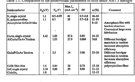
solar cells are their relatively low conversion efficiency, around 9% for good quality
amorphous silicon cells as shown in table 1.1 (6), and the high level o f technology
usually required to produce them. The vast majority o f solar cells are based on Silicon
in one form or another. The various most common technologies are presented in fig 1.1
(7). The world market for solar cells has been increasing rapidly since 1992, as shown
in fig 1.2 (7), and whilst this is only a small percentage o f the total world electrical use,
it is a good sign that we are heading towards cleaner energy.
Table 1.1. Comparison o f the Dhotovoltaic parameters o f cells under AM 1.5 sunlight
Semiconductor £ f(eV) V«(V)
Max/,c
(mA cm“2) FF *?(%) Comment
Si, single crystal 1.1 0.5-0.69 42 0.7-0.8 16-24
Si, polycrystalline Amorphous Si:Ge:H film
1.1 0.5 38 0.7-0.8 12-19
8-10 Amorphous film with
tandem structure. Convenient large area fabrication
GaAs, single crystal 1.42 1.03 27.6 0.85 24-25
AlGa As/GaAs Tandem 1.03 27.9 0.864 24.8 Different bandgap
materials in tandem increases absorption efficiency
GalnP/GaAs Tandem 2.5 14 0.86 25-30 Different bandgap
materials in tandem increases absorption efficiency
CdTc Thin film 1J5 0.84 26 0.73 15-16 polycrystalline films
InP, single crystal CuInSej
1.34 1.0
0.88 29 0.85 21-22
12-13
There are alternatives to the normal silicon based cells, one o f which is dye sensitised
metal oxide cell. These comprise a large bandgap semiconductor like Titanium Dioxide
with a dye adsorbed to harvest the light. This type o f cells promises simple technology,
and potentially useful light conversion efficiency (around 7% for a cell with a liquid
[image:13.614.55.488.298.560.2]makes this type o f cell far cheaper than many o f the other types o f cell. This research
will concentrate on optimising dye sensitised cells.
Si Rim
0.26% Amorphous Si I T 6.30%
CIS
0.18%
Cadmium Teiluride
0.42% Ribbon Si
3.50%
Single Ciystal Si 35.17% Poiycrystal Si
47.54%
Figure 1.1. Percentages o f the most common photovoltaic cell technologies.
450.0
400.0
350.0
300.0
as
| 250,0
CO
© 200,0
s
150.0
100.0
50,0
0,0
57,9 60,1 6 9 ^
-77*7- 88,6
T25t8
151,7
201,5
-384|3
--277;9
-, , ( ( ( ( ( ! f
1992 1993 1994 1995 1996 1997 1998 1999 2000 2001
[image:14.615.59.536.48.437.2]1.2. Aims and Objectives
• Develop and deposit semiconducting layers o f Titanium Dioxide (Ti02) with
and without an extended surface area made using a fine powder
• Characterise the semiconducting layers using a variety o f appropriate techniques
• Develop and deposit various thin dye layers adsorbed on different substrates by
various methods
• Characterise the dye layers using appropriate techniques
• Develop and attempt to optimise heterojunction solar cells based on the dye
layers adsorbed on the semiconducting layers
• Characterise the solar cells in terms o f efficiency, load characteristics, and
equivalent circuit model parameters.
• Design and produce an experimental setup capable o f measuring the lifetime o f
photogenerated carriers in thin films o f dye
1.3. Organisation of the Thesis
This thesis is comprised o f the following chapters; Introduction, Literature Review,
Theoretical Background, Experimental Methods, Result and Discussions, and
Conclusions and Suggestions for Further Work. The literature review chapter describes
published work that is relevant to this research, so that the reader m ay quantify this
work in terms o f other previous work. The theoretical background chapter presents any
mathematical methods used for data analysis, along with the physical theory o f selected
measurements techniques, and o f the operation o f solar cells. The experimental methods
chapter describes how each type o f sample was made, and practical information
regarding the measurements o f the samples. The results and discussions chapter
describes the results that were obtained, and discusses the implications o f the results and
how they compare with published work. The conclusions chapter compares the research
-aims with actual outcomes, describes how the research furthers academic knowledge,
and what work can be done to further this research.
Reference List
(1) http://www.nef.org.uk/greenenergy/biomass.htm accessed 17th June 2005
(2) http://www.nef.org.uk/greenenergy/geothermal.htm accessed 17th June 2005
(3) http://www.nef.org.uk/greenenergy/wind.htm accessed 17th June 2005
(4) http ://www.nef.org.uk/greenenergy/hydro.htm accessed 17th June 2005
(5) http://www.nef.org.uk/greenenergy/solar.htm accessed 17th June 2005
(6) Kasap S.O., 2001, Optoelectronics and Photonics : Principles and Practices.
Prentice Hall
(7) Goetzberger A., Hebling C., Schock H., Materials Science and Engineering
2003, R40, 1-46
-Chapter
Literature Review
2.1. Dye-Sensitised Solar Cells
Solar cells based on Titanium Dioxide films sensitised with a dye are a commonly
researched topic due to their being an interesting potential option as a cheap source o f
‘green’ electricity. Two main types o f dye sensitised Titanium Dioxide cell are studied;
those with an electrolyte and those without. Studies o f both types will be described, but
with emphasis on the type without an electrolyte (the ‘dry’ type).
2.1.1. Dye: Metal Oxide Cells in General
There are many published works on dye sensitised solar cells with a Ti02 layer that also
have a liquid layer. One such work ( 1) presented a cell comprised of; substrate/Sn02
nanopowder/Ruthenium dye/electrolyte/Pt. The cells were illuminated with a solar light
o f 200% ambient (such as that experienced using a condenser lens arrangement), and a
fill factor o f 65% and an efficiency o f 6% were achieved. Another such work (2)
presented a cell comprised o f substrate/ZnO nanopowder/Ru dye/LiI+I2/metal contact.
A fill factor o f 68% and an efficiency o f 5% was achieved at 10% o f full sunlight. It is
common to test cells at less than full sunlight as the cell might be used in low light
levels such as in buildings or in countries with little sunlight (such as England). The two
above results are typical o f the higher quality range o f wet dye sensitised cells.
There are even fewer published works on dye sensitised solar cells without a liquid
probably because o f the greater efficiency normally obtained with a wet cell. One o f
those published (3) presents a cell comprised o f Al/Al oxide/dye/Au (more details are in
a paper referenced by the authors). The cell obtained a fill factor o f 25% and an
efficiency o f 5x10^% at full sun. The low efficiency obtained is common to dry
sensitised cells and is probably due to insufficiently intimate contact between the top
metal and the dye. Where the wet cell has better efficiency, the dry cell has simplicity
and less likely to harm the environment by the leakage o f toxic chemical (the liquid
electrolyte).
2.1.2. Dye: T i0 2 Cells
There is much work published on dye sensitised T i0 2 solar cells with a liquid
electrolyte. One such study (4) demonstrated a cell made up of; FT0 /Ti02
nanopowder/Ruthenium dye/electrolyte/Pt. The cell achieved 67% fill factor and 0.22%
efficiency at 120% o f full sunlight. Another study (5) presented a cell with the design;
FTO (assumed)/Ti02 nanopowder(treated with TiCL*)/ Mercurochrome dye/KCl/Pt. The
cell gave a fill factor o f 73% at full sunlight, and an efficiency o f 1.44%. The most
commonly referenced work (6), is one o f the earliest works on modem dye sensitised
T i0 2, and it describes one o f the best qualities o f solar cell, giving a fill factor o f 68.5%
and an efficiency o f 7 .12% at full sunlight with a cell design of; F T 0 /T i0 2
nanopowder/Ruthenium dye/electrolyte/Pt. The majority o f modem cells are based on
this design.
There is also much work published on dye sensitised T i0 2 solar cells without a liquid
electrolyte. One such study (7) on the design; IT0 /Ti02/CuPc/Au gave a fill factor o f
about 25%, and an efficiency o f about 1.5xl0'4% under simulated solar light. Another
gave a fill factor o f 49% and an efficiency o f 0.8% under full sunlight illumination. Yet
another article (9) described a cell o f design; IT0 /Ti02/MEH-PPV/Au, with a fill factor
o f 67% and an efficiency o f 1.6%, but the illumination was only monochromatic light at
500nm.
It has been shown that a higher series resistance and a lower parallel resistance lead to a
lower fill factor (10). Since the fill factor has a significant effect on efficiency, it is
critical that a cell has low series resistance and a high parallel resistance (along with
various other good characteristics) to have a useful efficiency. The ideality factor o f dye
sensitised solar cells normally ranges from 1.5 to 2 (11-13), when analysed with the
one-diode model. The reverse saturation current has been shown to vary in the range
from 15nA to 30nA for a particular design, the series resistance can vary in the range
2.5H to 14211, and the parallel resistance can vary in the range 1.3kl2 to 61kl2. The
diode ideality factor has been shown (14) to fall outside the above range, with a value o f
2.9, and a corresponding value o f saturation current o f 1.15nA.
2.2. Titanium Dioxide Thin Films
The inorganic layer o f the cell studied in this research is comprised o f a very thin
( < 200nm) layer o f non-porous Ti02 to cover the bottom contact and prevent short
circuits, onto which is deposited a thicker (around 10/mi) porous film to give an
extended area o f interface. Much work has been done to study such films made and
2.2.1. Sputtered
There is a great wealth o f published work on Ti02 produced by sputtering with various
parameters (such as with R f or DC power supply, or whether the target is metallic or a
sub-oxide o f Titania). The work on RF sputtering will be summarised first. AFM
images o f thin films o f Ti02 have been obtained (15; 16) that show grain sizes in the
range 60nm to 176nm with roughness in the range 2.1nm to 6 .6nm. X-Ray Diffraction
(XRD) spectra have been presented (15-18) for samples produced with various substrate
heating from ambient to 1000°C. It is shown that without heating, Anatase is the only
phase present, and with heating above about 350°C, the Rutile phase begins to manifest
and increasingly so with extra heating up to 1000°C, where the Rutile phase dominates.
Stoichiometry has been determined for various TiC>2 thin films by X-ray Photoelectron
Spectroscopy (XPS) (19;20). It shows that with and without annealing at temperatures
o f up to 500°C, the films remain fully or very nearly fully stoichiometric with a ratio o f
two atoms o f Oxygen to every one atom o f Titanium. SEM images have shown (20) that
the microstructure o f a Ti02 thin film can change from one o f higher porosity to one o f
higher density when the oxygen partial pressure and total pressure decrease and the RF
power (and thus sputtered particle kinetic energy) increase. Titanium oxide films o f
greatly varying conductivity have been presented (21;22). For Ti02 , a conductivity o f
9.4x1 O ^ Q 'W 1 was given, whilst for sub oxides o f TiOx where x = 0.75 to 1.45,
conductivities in the range 3076Q’1m‘1 to 111 lQ ^ m ’1 respectively were given. These
correspond well with the conductivity o f TiO which is stated as 2500Q '1m '1. Refractive
index and extinction coefficient spectra have been published (17;23) and give wide
variation depending on e.g. pressure, power and annealing temperature. At 600nm,
refractive index has been shown to vary from 2.1 to 2.4, and extinction coefficient has
been shown to vary from 0.001 to 0.016. This shows that the optical properties o f thin
The work on DC sputtered films will now be presented. AFM images have shown
(24;25) that the grain size for DC sputtered films can vary from about 40nm to an
average o f 143nm and can have a complex dependency on the temperature o f the
substrate during deposition. The crystallinity o f thin Ti02 films have been determined
(26-29) by their XRD spectra. For films with substrate heating during deposition o f up
to 220°C, only the Anatase phase was observed. For films with substrate heating o f
620K, a mixture o f Anatase and Rutile phases were observed, where the ratio o f the
phases was seen to be dependent (in part) on the stoichiometry (which was controlled
by the plasma emission), and the phase transforms entirely to Rutile by annealing at
1070K. Films produced by a pulsed (25kHz to 40kHz) DC supply show the Rutile phase
with substrate temperature as low as 200°C. Stoichiometry o f Ti02 sputtered films has
been determined from XPS spectra (30;31). For XPS measurements, the authors will
generally use a ceramic or nonstoichiometric target, which has been shown to give
higher depositions rates. It has been shown that sputtering from a nonstoichiometric
target with a low oxygen mole fraction in the sputtering gas will yield a stoichiometric
film, whilst for a higher oxygen fraction, there is a deviation from stoichiometry. The
details observed by SEM show (32;33) a general (and often seen) columnar growth
pattern and a rough surface (in the sub-microscopic range) o f grains size o f
approximately 9.2nm for films deposited at room temperature and growing to
approximately 46.2nm for films deposited at 220°C. A wide range o f conductivities
have been measured (24;25) for films under various conditions; effective multi layer
films o f Ti02 with embedded Ti gave transparent films with high conductivity (relative
to pure TiC>2) in the range lO f i'W 1 to lOOOO^m’1, films o f thickness in the range
230nm to 450nm had a conductivity in the range 0.312 'lm l to 23912' W 1 which was
dependant on substrate temperature, deposition rate and weight percentage o f Anatase
extinction coefficient have been studied (34;35) and have been shown to vary
somewhat; n can vary from 2.43 to 2.58 with temperature and from 2.1 to 2.3 with
oxygen mole fraction in the sputtering gas, and k can vary from 0.000 to 0.03 with
temperature and from 0.002 to 0.002 with oxygen mole fraction in the sputtering gas.
The majority o f published work detailing the band gap type extracted as a parameter in
the Tauc model assumes a particular value for the index n, usually either 0.5 or 2. As
many films o f sputtered TiC>2 show some amorphicity, it is perhaps better to extract the
real value o f the parameter and then discuss it. The bandgap type has been obtained
(36;37) as 0.5 (direct allowed) with a bandgap o f 3.27eV at 300K (compared with other
work the authors referenced giving between 3.02 and 3.54eV), and as 2 (indirect
allowed) with a bandgap o f 3.34eV to 3.39eV. M ost authors usually obtain the index by
plotting the data to the power o f the index reciprocal; if the graph is linear, the index is
correct and parameters can be obtained from the linear portion.
2.2.2. N ano Pow der
Surface morphology o f nanoporous films has been studied by AFM and SEM (38;39),
at two ranges o f magnification and o f two different types o f samples; those with
irregular space in TiC>2 mass and those with irregular TiC>2 mass in space (an analogy is
a sponge for the former and a layer o f granules for the latter). The sponge type films
were made by using tetrabutylorthotitanate and polyethylene glycol (PEG) as a
precursor and template, respectively, and the effect o f the amounts o f PEG and other
complexing agents (such as diethanolamine) on the structure were observed. The SEM
images show that pore size depends on the molecular weight o f PEG used; 2.0 g PEG
(1000)/100 ml gives a mean pore size o f 186nm, whilst 4.0 g PEG (1000)/100 ml gives
a mean pore size o f 684nm. Changing the complexing agents changes the structure from
acid - H3L). The granule type films were produced by autoclaving a mixture o f
40mg/ml Degussa P25/water at 200°C for between one and ten days. The suspension
was then applied to a glass substrate via a simple doctor-blading method and sintered at
450°C for 30 min. The SEM images show that the homogeneity (in terms o f particle
size and roughness) o f the films improves after longer times o f autoclaving the
suspension. The AFM images also show this, and show a particle size in the region o f
80nm. Roughness values were in the region o f 20nm and were highest for
nonautoclaved P25. Conductivities for different samples o f nanoparticle films have been
studied for their electrical characteristics (40;41). Nanoporous films o f Ti02 were
manufactured by a chemical method and some were annealed in hydrogen at 400°C for
15minutes to create oxygen vacancies. The average particle size was in the range o f
lOnm to 15nm. The conductivities o f as-prepared samples and annealed samples were
measured and were found to be dependent on temperature, with the as-prepared sample
having a room temperature conductivity o f l.S Q ^ m '1, and the annealed sample having a
room temperature conductivity o f 0.040Q '1m '1. The conductivities at higher temperature
(673K) became similar. Films o f nanoporous TiC>2 o f 50% porosity and particle size in
the range lOnm to 15nm have been made by in-house synthesis and studied for
photoconductivity in under various conditions. Resistivity was found to be in the order
o f 104Qm to 106Qm in dark and in ambient air. This falls by 102 to 103 times when
measured under vacuum which the authors tentatively attribute to removal o f water
which may dope the film with protons. Photoconductivity is 106 times larger in vacuum
than in air and increases with decreasing pressure, which the authors attribute to the loss
o f surface adsorbed oxygen. The authors used a 75 W xenon lamp for illuminating the
2.3. Dyes an d O th e r Layers
The dye is the layer that absorbs the light, although only a portion o f the solar spectrum
is actually absorbed due to an incomplete absorption spectrum that occurs in most dyes.
Published work on the dyes used in this research is presented below.
2.3.1. CuPc, Rose Bengale, poly(9-vinylcarbazole) (PVK)
Absorption spectra o f various Metal Phthalocyanines have been studied in different
chemical and physical environments. Dyes in solution, such as that shown in fig 2.1
(42), may have quite narrow peaks, with CuPc being more absorbent near the main
peak, whereas dyes spun coated, such as that shown in fig 2.2 (42), m ay be much
broader with a greatly diminished main peak.
ZnPc RuPc CuOHPc
2.0
a u c
CD _QL_
o to
0.5
0.0
560 580 600 620 640 660 680 700
Wavelength (nm)
2.0
ZnPc
RuPc
□
CuPcOH <D
o c
ro s i
O (/) Si < 0 .5
0.0
55 0 6 0 0 6 5 0 700 750 80 0
W a v elen g th (nm)
Figure 2.2. UV-Vis spectra o f Spin coated films o f Metal Phthalocyanines about lOOnm thick
Reference (CuPc/H2S 0 4)
MET2
ACD2
o
1.0-FOR2
0 .5
-0.0
4 0 0 5 0 0 6 0 0 7 0 0 8 0 0 9 0 0
W a v elen g th (nm )
Figure 2.3 U V -V IS absorption spectra for C uP c-S i02 composites with different chemical processing. Reference o f CuPc dissolved in H2SO4 shown.
Absorption spectra o f various Metal Phthalocyanines have been studied in different
composites and solvents such as H2SO4 and give results such as that in fig 2.3 (43).
H2SO4 shifts the main absorbance peak to the right by about 150nm relative to CuPc in
Chloroform. The environment that the dye is in clearly changes its optical
-characteristics, and it can be worth studying a dye deposited on different layers to
determine the properties o f the dye as part o f a device in addition to the dye in isolation.
Absorption spectra o f Rose Bengale in different environments have been studied and
give results such as that fig 2.4 (44). It was seen that the spectrum o f Rose Bengal
dissolved in water is quite different from that adsorbed onto a polymer (mostly in terms
o f the relative peak heights and shapes - not the overall height difference which is
mostly due to the light passing through a different amount o f dye).
2.5
_Q
' 4 00 5 0 0 6 0 0 7 0 0
W avelength (nm)
Figure 2.4. UV/VIS spectra o f (a) Rose Bengal in water and (b) Rose Bengal bound to poly(N-vinylpyrrolidone).
The measured spectrum o f Rose Bengal in ethanol in fig 2.5 (45) is quite different from
that in plain water - the main peak o f the spectrum in ethanol is much higher than that in
water. As with the CuPc studies, it is seen that the environment o f the dye changes its
optical characteristics significantly. PVK is visually transparent and thus, absorption
g 0.8
03
■e 0.6
-9 0.4
0.2
4 0 0
W avelength (nm)
[image:27.612.81.464.16.228.2]200
30 0 500 600 700Figure 2.5. UV-Vis spectrum o f Rose Bengal in ethanol
The electrical conductivity o f CuPc and its dependency on gaseous atmosphere and
temperature has been studied (46) and has been found to vary from lO ^fl^m ' 1 to
lO ^O ^m '1, rising with temperature. Activation energy, Ea, varied with atmosphere from
0.54eV to 1.1 eV. Another study (47) which used a CuPc layer as a electrical gas sensing
element by thermally evaporating CuPc onto an interdigitated electrode, gave an
electrical conductivity o f about 2 5 0 x l0 '6Q‘1m‘1, which rose by 75 times when exposed
to 3 parts per million o f NO2, and is the same range as the previous study.
Little work could be found that described the conductivity o f PVK (which is actually
quite a commonly used hole transport material in dye sensitised solar cells), but one
study (48) showed a temperature dependence o f conductivity, but the response was such
that at room temperature, the conductivity was in the order o f 10"150 _1m_1 which seems
unreasonable. Rose Bengal is used often in medicine to detect damage to the eye (bad
areas are stained while good areas are not). Its use in physics research is fairly new, and
2.3.2. O th e r C om m only Used Chem icals
Out o f the over 100 dyes used for solar cells, by far the most common dyes that
scientists use are based on a Ruthenium complex (with the most common complex
being cis-dithiocyanto-bis[2,2'-bipyridyl 4,4'-dicarboxylate] Ru(II)). The Ru dyes
strongly absorb light in low wavelengths, (unlike CuPc and Rose Bengal), but cost
around £2000 per gram (49). Other dyes used include porphyrin (50), Chloropyll (51),
and Santalin (52) from sandalwood. The electrolytes used in 'wet' cells have advantages
and disadvantages; on one hand they give great penetration o f the porous dye-covered
layers w ith subsequent high extraction o f carriers and good conversion efficiency, but
on the other hand they are toxic, and prone to leak out o f the cell even i f it is sealed
(over time any sealant will degrade and crack) and the cell m ay break (it is made o f
glass after all) and spill the electrolyte onto the ground or into the loft space o f a house
it is installed on. Such spillage could be disastrous. Many scientists have tried to used a
thicker form o f electrolyte or to dispense with an electrolyte altogether and apply a solid
(as a solution that dries leaving the material penetrating the pores) conducting layer to
carry away the photogenerated holes. Examples o f such hole conducting layers are;
poly(3-octyltiophene) (P30T) (53), Copper Iodide (52), p o ly [3 -(ll diethylphosphoryl-
undecyl) thiophene] (abbrev. P3PUT), poly(4-undecyl-2,2'-bithiophene), (abbrev.
P4UBT), poly(3-undecyl-2,2'-bithiophene) (abbrev. P3UBT) (54).
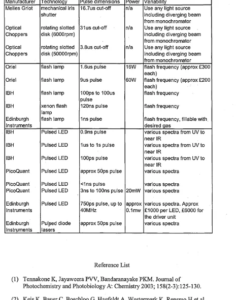
2.4. L ight M odulation
Application o f pulses o f light to a sample is a common way o f exciting the sample. As
such, there is a plethora o f ways o f producing light from mechanical modulators like
choppers that intermittently interrupt a light source, to pulsed LEDs that operate in the
tens o f picoseconds time regime. The time regime needed will depend on the type o f
o f light in different time regimes and in different ways is shown in table 2.1, to give the
reader a better appreciation o f the range o f capabilities, technologies and cost o f various
commercial light pulse generators. The data was mostly obtained from company
websites and technical queries. Lifetimes o f Titanium oxides have been shown (55;56)
to vary across several orders o f magnitude from nanoseconds to microseconds
(dependent on such parameters as Platinum doping level), and lifetimes in other
semiconductors have been shown (57) to vary from lp s to 10ns (depending on doping
levels o f Zinc and Carbon). Clearly, if one system is to be able to study all types o f
samples, it must be able to deal with at least six orders o f magnitude o f variance in
lifetime. Lifetimes have been measured by various means including photoluminescence
Table 2.1. A review o f a selection o f commercial optical modulators
Manufacturer Technology Pulse dimensions Power Variability
Melles Griot mechanical iris
shutter
16.7us cut-off n/a Use any light source
including diverging beam from monochromator Optical
Choppers
rotating slotted disk (6000rpm)
31 us cut-off n/a Use any light source
including diverging beam from monochromator Optical
Choppers
rotating slotted disk (50000rpm)
3.8us cut-off n/a Use any light source
including diverging beam from monochromator
Oriel flash lamp 1.6us pulse 16W flash frequency (approx £300
each)
Oriel flash lamp 9us pulse 60W flash frequency (approx £200
each)
IBH flash lamp 100ps to 100us
pulse
flash frequency
IBH xenon flash
lamp
120ns pulse flash frequency
Edinburgh Instruments
flash lamp 1ns pulse flash frequency, fillable with,
desired gas
IBH Pulsed LED 0.9ns pulse various spectra from UV to
near IR
IBH Pulsed LED 1 us to 1s pulse various spectra from UV to
near IR
IBH Pulsed LED 100ps pulse various spectra from UV to
nearIR
PicoQuant Pulsed LED approx 50ps pulse various spectra
PicoQuant Pulsed LED <1ns pulse various spectra
PicoQuant Pulsed LED 3ns to 100ns pulse 20mW various spectra
Edinburgh Pulsed LED 750ps pulse, up to approx various spectra. Approx
Instruments 40MHz 0.1 mw £1000 per LED, £6000 for
the driver unit Edinburgh
Instruments
Pul?ed diode lasers
approx 50ps pulse various spectra
Reference List
(1) Tennakone K, Jayaweera PVV, Bandaranayake PKM. Journal o f
Photochemistry and Photobiology A': Chemistry 2003; 158(2-3):125-130.
(2) Keis K, Bauer C, Boschloo G, Hagfeldt A, Westermark K, Rensmo H et al. Journal o f Photochemistry and Photobiology A: Chemistry 2002; 148(l-3):57- 64.
(3) Nevin W, Chamberlain G. IEEE Transactions on Electron Devices 1993; 40(1):75.
(4) Nogueira AF, De Paoli MA. Solar Energy Materials and Solar Cells 2000; 61(2):135-141.
-(5) Hara K, Horiguchi T, Kinoshita T, Sayama K, Sugihara H, Arakawa H. Solar Energy Materials and Solar Cells 2000; 64(2): 115-134.
(6) Regan B, Gratzel M. Nature 1991; 353:737.
(7) Tracey S, Ray A, Shishiyanu T. IEE Procedings 1998; 145(5):383.
(8) Senadeera GKR, Jayaweera PVV, Perera VPS, Tennakone K. Solar Energy . Materials and Solar Cells 2002; 73(1): 103-108.
(9) Fan Q, McQuillin B, Bradley DDC, Whitelegg S, Seddon AB. Chemical Physics Letters 2001; 347(4-6):325-330.
(10) Yeon Song M, Kim KJ, Kim DY. Solar Energy Materials and Solar Cells 2005; 85(1):31-39.
(11) Boschloo G, Lindstrom H, Magnusson E, Holmberg A, Hagfeldt A. Journal o f Photochemistry and Photobiology A: Chemistry 2002; 148(1-3):11-15.
(12) Frank J, Kopidakis N, Lagemaat Jvd. Coordination Chemistry Reviews 2004; 248(13-14): 1165-1179.
(13) Hagfeldt A, Boschloo G, Lindstrom H, Figgemeier E, Holmberg A, Aranyos V et al. Coordination Chemistry Reviews 2004; 248(13-14): 1501-1509.
(14) Grant CD, Schwartzberg AM, Smestad GP, Kowalik J, Tolbert LM, Zhang JZ. Synthetic Metals 2003; 132(2): 197-204.
(15) Mardare D, Rusu GI. Materials Science and Engineering B 2000; 75(1):68-71.
(16) Jeong B-S, Budai JD, Norton DP. Thin Solid Films 2002; 422(1-2):166-169.
(17) Amor SB, Guedri L, Baud G, Jacquet M, Ghedira M. Materials Chemistry and Physics 2003; 77(3):903-911.
(18) Hiratani M, Kadoshima M, Hirano T, Shimamoto Y, Matsui Y, Nabatame T et al. Applied Surface Science 2003; 207(1-4):13-19.
(19) Chow LLW, Yuen MMF, Chan PCH, Cheung AT. Sensors and Actuators B: Chemical 2001; 76(l-3):310-315.
(20) Ben Amor S, Baud G, Jacquet M, Pichon N. Surface and Coatings Technology 1998; 102(l-2):63-72.
(21) Banakh O, Schmid PE, Sanjines R, Levy F. Surface and Coatings Technology 2002; 151-152:272-275.
(22) Mardare D, Rusu GI. Materials Science and Engineering B 2000; 75(1):68-71.
(23) Amor SB, Baud G, Besse JP, Jacquet M. Materials Science and Engineering B 1997; 47(2): 110-118.
(25) Springer SG, Schmid PE, Sanjines R, Levy F. Surface and Coatings Technology 2002; 151-152:51-54.
(26) Radecka M, Zakrzewska K, Brudnik A, Posadowski W. Thin Solid Films 1999; 343-344:152-155.
(27) Lapostolle F, Huu Loi T, Billard A, Frantz C. Surface and Coatings Technology 1997; 97(l-3):574-581.
(28) Treichel O, K irchhoff V. Surface and Coatings Technology 2000; 123(2-3):268- 272.
(29) Takeda S, Suzuki S, Odaka H, Hosono H. Thin Solid Films 2001; 392(2):338- 344.
(30) Ohsaki H, Tachibana Y, Mitsui A, Kamiyama T, Hayashi Y. Thin Solid Films 2001; 392(2):169-173.
(31) Tomaszewski H, Poelman H, Depla D, Poelman D, De Gryse R, Fiermans L et al. Vacuum 2002; 68(l):31-38.
(32) Takeda S, Suzuki S, Odaka H, Hosono H. Thin Solid Films 2001; 392(2):338- 344.
(33) Viseu TMR, Almeida B, Stchakovsky M, Drevillon B, Ferreira MIC, Sousa JB. Thin Solid Films 2001; 401(l-2):216-224.
(34) Vergohl M, Malkomes N, Staedler T, Matthee T, Richter U. Thin Solid Films 1999; 351(l-2):42-47.
(35) Tomaszewski H, Poelman H, Depla D, Poelman D, De Gryse R, Fiermans L et al. Vacuum 2002; 68(l):31-38.
(36) Miao L, Jin P, Kaneko K, Terai A, Nabatova-Gabain N, Tanemura S. Applied Surface Science 2003; 212-213:255-263.
(37) Dannenberg R, Greene P. Thin Solid Films 2000; 360(1-2): 122-127.
(38) Kontos Al, Arabatzis IM, Tsoukleris DS, Kontos AG, Bernard MC, Petrakis DE et al. Catalysis Today 2005; 101(3-4):275-281.
(39) Bu SJ, Jin ZG, Liu XX, Yang LR, Cheng ZJ. Journal o f the European Ceramic Society 2005; 25(5):673-679.
(40) Madhusudan Reddy K, Manorama S V, Ramachandra Reddy A. Materials Chemistry and Physics 2003; 78(l):239-245.
(41) Eppler AM, Ballard IM, Nelson J. Physica E: Low-dimensional Systems and Nanostructures 2002; 14(1-2): 197-202.
(42) Spadavecchia J, Ciccarella G, Vasapollo G, Siciliano P, Rella R. Sensors and Actuators B: Chemical 2004; 100(1-2): 135-138.
(43) Litran R, Ramirez-del-Solar M, Blanco E. Journal o f Non-Crystalline Solids 2003; 318(l-2):49-55.
-Gigimol M, Mathew B. Polymer International 2003; 52:973-980.
Du H, Fuh R, Li J, Corkan A, Lindsey J. Photochemistry and Photobiology 1998;68:141-142.
Zhivkov I, Spassova E, Dimov D, Danev G. Vacuum 2004; 76(2-3):237-240.
Newton MI, Starke TKH, Willis MR, McHale G. Sensors and Actuators B: Chemical 2000; 67(3):307-311.
Tayyan A, Khogali A. CHINESE JOURNAL OF PHYSICS 2004; 42(4):392- 400.
htto://www.solaronix.com/oroducts/Chemicals/specialtv.html. accessed June 2005.
M a T, Inoue K, Noma H, Yao K, Abe E. Journal o f Photochemistry and Photobiology A: Chemistry 2002; 152(l-3):207-212.
Kumarasinghe AR, Flavell WR. Journal o f Photochemistry and Photobiology A: Chemistry 2002; 148(1-3):145-151.
Tennakone K, Kumara GRRA, Kottegoda IRM, Perera VPS, W eerasundara PSRS. Journal o f Photochemistry and Photobiology A: Chemistry 1998;
117(2): 137-142.
Gebeyehu D, Brabec CJ, Sariciftci NS, Vangeneugden D, Kiebooms R, Vanderzande D et al. Synthetic Metals 2001; 125(3):279-287.
Smestad GP, Spiekermann S, Kowalik J, Grant CD, Schwartzberg AM, Zhang J et al. Solar Energy Materials and Solar Cells 2003; 76(1):85-105.
Wilke K, Breuer HD. Journal o f Photochemistry and Photobiology A: Chemistry 1999; 121(l):49-53.
Kim SC, Heo MC, Hahn SH, Lee CW, Joo JH, Kim JS et al. Materials Letters 2005; 59(16):2059-2063.
Chapter
Theoretical Background
3.1. Structural characteristics
This section describes the structural aspects o f materials, such as what is meant by
crystallinity, and what may be seen at different levels o f magnification. There is
sufficient depth that the reader may better understand the presented results in chapter 5.
3.1.1. Crystallographic Phase
A crystal is a solid, and a periodic arrangement o f atoms or molecules that is comprised
o f repeated instances o f a basic "unit cell", in three dimensions (1). Not all solids are
crystalline; glass for example is amorphous and shows no periodicity in its atomic
layout. M any solids are comprised o f a mosaic o f crystals with different orientations to
one another, but each crystal will have periodicity matching the periodicity o f the rest o f
the crystals. A solid comprised o f a single crystal (like a silicon wafer made for the IC
industry) is termed "monocrystalline", while one that is comprised o f m any crystals
(like cast iron) is termed "polycrystalline". Each crystalline material will arrange in a
very specific way. For example, some crystals arrange such that each atom or molecule
lies at the comers o f a cube, while others arrange such that each atom or molecule lies at
the comers or centre o f a cuboid. The specific way that a crystalline material arranges is
known as its 'phase'. Some materials can exist in more than one phase, with TiC>2 being
There are seven different crystal systems; cubic (three axes, all equal length), tetragonal
(three axes, two equal length), orthorhombic (three axes, non equal length),
rhombohedral (three axes, equal length, equal angles o f inclination), monoclinic (three
unequal axes, one angle not a right angle), triclinic (three unequal axes none at right
angles), and hexagonal (two equal coplanar axes at 120°, third (not equal) at right
angles). Some systems are subdivided into other types due to additional atoms at the
base centre, face centre, or body centre. In total there are 14 lattice types collectively
known as the Bravais Lattices, each o f which define not only the lattice structure (in
terms o f relative positions and parameters) but also the unit cells that make up the
lattices. Two examples o f unit cells are given in fig 3.1, with the important lattice
parameters shown. The type o f unit cell and the particular values o f the lattice
parameters define the phase o f a material. The lengths o f the sides o f the cell and
internal angles are labelled a, b, c, a , p, y, respectively.
an atom
an atom
Figure 3.1. Body-centred orthorhombic (left) and triclinic (right).
The atoms in a lattice form planes that will diffract incoming X-Ray beams at certain
directions, in a vaguely similar manner to a mirror (this is explained in detail later).
Each plane has its orientation defined by a set o f numbers called M iller Indices (the
indices are labelled [hkl] for a 3D lattice). Each M iller Index is equal to the reciprocal
o f the fraction o f the point o f intersection o f the plane to an axis, to the length o f the
-axis. Negative values having a bar placed above the index. It is better explained by the
following relation;
a x is len gth
M ille r In d ex = (3.1)
p o i n t o f in te r c e p t
If a plane lies parallel to an axis, it will never cross it, so the point o f intercept is
infinity, and the corresponding index is zero. Each lattice type has an associated
equation relating the miller indices, the interplanar thickness and the dimension o f the
unit cell. A selection is given below;
1 h 2 + k 2 + l 2 Cubic:
Tetragonal: 1 _ h 2 + k 2 d 2 ~
V 2 + ~
a c
1 h 2 k 2 12 Orthorhombic: — = — h— r
d a 2 1 7 ,2 b * ' 2c
(3.2)
(3.3)
(3.4)
A selection o f planes through a simple lattice, each plane being parallel to the z-axis in
the page, is shown in fig 3.2. It is obvious that as the angle o f the plane changes from
flat to a large angle, the distance between the planes (interplanar distance) decreases.
This is proved later.
[
10
]
[ii]
[
21
]
3.1.2. Microscopic and Nanoscopic Details
Microscopic details are those that have a size in the order o f micrometres. Such details
may include specks o f dust or pollen on the sample surface or trapped within one o f the
layers, or tiny cracks and fissures or ‘pinholes’ that are beyond the range o f human
eyesight. The presence o f such details can be devastating to the operation o f a device
especially those whose layers are thinner than the detail’s size. A speck o f dust can blot
out many hundreds o f devices in a modem VLSI circuit, and may destroy the order o f a
very thin multi layer device possibly causing device failure. Nanoscopic details are
those that have a size range in the order o f nanometres (sub-micrometer). Such details
may include individual grains in a polycrystalline sample, or the step at the start o f a
layer on a substrate. Details at these size ranges are not visible through an ordinary
optical microscope. There exist other types o f microscope, such as the atomic force
microscope that can allow an observer to observe details in the nanometre size range.
If details such as dust specks are seen in a sample, then this can be indicative o f poor
sample preparation due to insufficient air filtering in a clean room for example. A
network o f fine cracks can be the result o f excess shrinkage when a sample is annealed
in an oven. A qualitative analysis o f the porosity o f a powder sample m ay be made at
this range. The size o f the grains can have a significant effect on the properties o f a
device, so to know the grain size distribution o f a sample can be useful in identifying
reasons for certain characteristics o f some data. The presence o f nanoscopic particles o f
one material in another, smooth or amorphous material can show up in nanoscopic
3.1.3. Stoichiometry
Stoichiometry is the study o f the ratios o f elements in a reaction to balance the chemical
equation. In the case o f this research, the stoichiometry just refers to the ratio o f
elements in a sample i.e. 2 moles o f Oxygen for every 1 mole o f Titanium will produce
a sample o f Titanium Dioxide with correct stoichiometry, and the sample can be said to
be stoichiometric.
I f the sample has incorrect stoichiometry, then its properties can change considerably.
Excess Titanium will make the film appear shiny and darker, reducing the amount o f
light that penetrates it (while at the same time increasing the conductivity). Excess
Oxygen can lead to trapping o f electrons, and because the Ti02 side o f the solar cell is
where the photogenerated electrons move to, any trapping effects will reduce the
efficiency o f the cell.
3.2. Electrical Characteristics
This section describes the electrical aspects o f materials and device, such as how the
heterojunction solar cell differs from the homojunction solar cell, and how the diode
model parameters are extracted by a fitting algorithm.
3.2.1. Conventional Solid State Solar Cell
Conventional solar cells are made o f a homojunction device, which is to say that it is
from one piece o f material that the junction and the areas to each side are made (2).
Assuming that a silicon wafer cell (the most common type) is being studied, the
junction is made by heavily doping one side n-type (electrons are the majority carriers),
and doping the other side p-type (holes are the majority carriers). A schematic (not to
short
drift
medium
' © © •diffusion
long
0 ©depletion
region
neutral
[image:39.612.65.499.22.263.2]n-region
p-region
neutral
Figure 3.3. A schematic diagram o f a silicon solar cell showing carrier transport.
The sunlight is incident on the n side and photons can be absorbed in the n region if
they are short wavelengths, in the depletion region (the area depleted o f carriers) if they
are o f medium wavelength, or in the p-region if they are o f long wavelength. The place
where the photons are absorbed is not some fixed distance, but a most probable distance
based on the likelihood o f absorption (shorter wavelengths will be absorbed with a high
probability and so will tend to be absorbed after a shorter journey, hence, in the n-
region). When a sufficiently energetic photon is absorbed, an electron-hole pair is
created and the electron will diffuse to the boundary with the depletion layer before
drifting across (due to the built in potential created by the ionised atoms from which
carriers have been removed) to the n-region, to make it more negative and vice versa for
the holes. A voltage (called the photovoltage) is thus produce across the terminals o f the
device, which may be connected to a load to do work. Any accumulated electrons in the
n-region will travel through the load to recombine with the holes in the p-region. The
smaller the load, the more current will be supplied by the device, but this lowers the
photovoltage as the carriers producing the voltage are being removed by the load. The
-n-region is heavily doped so as to make it thinner than the p-region, as the
photogenerated holes diffuse a shorter length before recombination compared to the
electrons and vice-versa.
3.2.2. Dye Sensitised Solar Cell
A deep theoretical analysis o f the function o f a heterojunction will not be presented
here, as it is not within the scope o f this work. Instead, a summary o f the theory
presented by previous Ph.D. research (3) will be described. This will give the reader
sufficient understanding o f the workings o f the heterojunction to better understand the
results and the implications o f them.
The adsorbed dye is photoexcited by an incident photon and produces a free electron,
which will diffuse to the junction and is then injected into the conduction band o f the
semiconductor it is deposited on, leaving behind a free hole in the valence band o f the
dye. Electrons coming back from the load m ay fill these holes. Direct photogeneration
o f the electron is rare in Phthalocyanines, and it is most likely that the absorbed photon
produces a loosely bound electron that can dissociate at a free surface, or at an internal
dissociation point such as an impurity. In a typical heterojunction cell, there may be
several current transfer mechanisms occurring in addition to the injection, such as
generation-recombination, and recombination at interface states at the junction.
The semiconductor in the case o f all dye sensitised work is transparent in the visible
region, and will therefore absorb only a very small amount o f sunlight - that o f low
wavelength (below around 300nm), meaning the dye must absorb as much light as
possible. This is quite different to the homojunction cell described above, where all o f
bands o f wavelength, so to absorb most o f the light, several dyes must be used (either
simply mixed together or made up as a tandem cell).
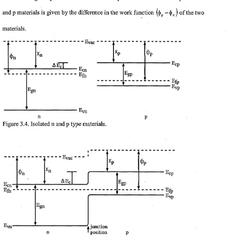
Band diagrams o f separate n and p materials (Ti02 and CuPc respectively in this case)
and joined n and p materials are shown in fig 3.4 and fig 3.5 respectively. It was
assumed that the electron affinity o f the n type material was greater than that for the p
type material. When the materials are joined (when the CuPc is deposited on the TiCh
surface), the Fermi levels shift such that they coincide. This shifts the rest o f the energy
levels forming a step in the bands. The built-in potential that is created by the union o f n
and p materials is given by the difference in the work function ((|)p — (|)n) o f the two
materials.
vac
n
xp 4>P
Egp
■^cp
--- ^lp
Figure 3.4. Isolated n and p type materials.
[image:41.616.75.521.250.715.2]junction position
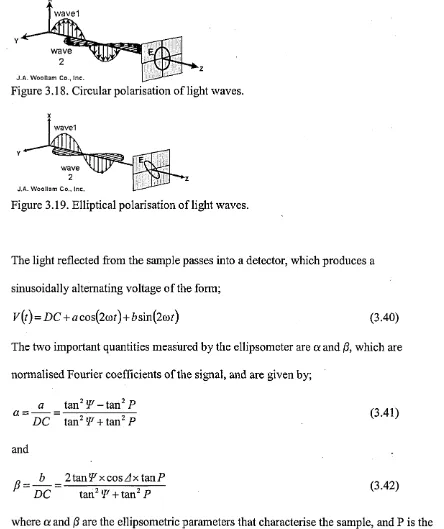
A photovoltaic cell acts as a diode in parallel with a current generator that is light
intensity dependent. This gives the cell diode-like characteristics with a negative current
offset due to the photovoltaic effect. By varying the load that the cell is connected to,
the cell output can be varied from zero voltage with maximum current (giving Isc with
short circuit load) to zero current with maximum voltage (giving Voc with open circuit
load), both extreme states giving no power to the load, as the power is the product o f
current and voltage. At any other load resistance, the power will be non-zero and at
some load value, there will be a maximum power delivered to the load. The ratio o f the
maximum output power to the product o f Isc and Voc is termed the fill factor o f the
device. A low fill factor will limit the efficiency.
The fill factor can be calculated by inducing a photovoltage in a cell, connecting it to a
variable load, and then measuring the photo voltage at different loads. The photocurrent
(usually a much smaller value than photovoltage) can then be calculated and the
maximum power can be obtained, and the fill factor determined. An example o f this
process is shown in fig 3.6 for simulated data. Voc = 0.502V, Isc =100/liA, VWOrk =
0.428V, IWork = 94.3/iA, giving a fill factor value o f 0.804, or 80.4%. The best load is
4.54kfi. This means that when this cell is illuminated, only 80.4% o f all the available
electrical energy it produces can be used. The fill factor for many devices is much less
than this.
-Voltage (V)
0 - J 50.0
0 6 - 40.0 5
- 30.0 |
- 20.0 I
em
power - 10.0
0.0
Figure 3.6. Simulated cell response with varying load. Load line at maximum power shown.
It was believed that the heterojunction cell had the same current-voltage model (and
thus the same equivalent circuit) as the homojunction cell, also incorporating series and
parallel resistance and ideality factor, and this model is shown below.
3.2.3. Diode Model Fitting
A simple PN junction (a device comprised o f a semiconductor where one half is doped
with acceptor impurities - p type, and the other h alf is doped with donor impurities - n
type) has electrical characteristics that can be described by the universal diode equation;
where V is the voltage across the PN junction, Is is the reverse saturation current, k is
the Boltzmann constant, n is the ideality factor, T is the ambient temperature, and q is
the electron charge.
A real solar cell has a photovoltaic current and some resistance that is in series with the
cell, and therefore the basic diode equation must be modified as follows (2);
(3.6)
-where Iph is the generated photovoltaic current, and JRS is the voltage drop across the
series resistance Rs. Solar cells have a parallel resistance that manifests itself as a
detrimental effect on the quality o f the solar cell.
There is a resistance, Rp, in parallel with the device and the effect o f this (when it
dominates) is to make the cell look like a resistor o f value Rp. Rp can be determined as
the reciprocal o f the gradient o f the I(V) graph in the negative voltage range. Similarly,
Rs can be determined (though with somewhat more difficulty) as the reciprocal o f the
gradient o f the I(V) spectra in the positive voltage range when it tends towards linearity.
The values o f n and Is can be found by taking natural logs o f the I values, and plotting
against V, which will result in a plot that tends towards linear. The gradient o f the linear
section o f the plot yields q/nkT, and the intercept yields natural log o f Is.
Whilst the above procedure for extracting the parameters o f the model works fairly well
with error-free data and with the parameters meeting certain criteria, a much better
method is to perform the extraction by a curve fitting procedure. Such a procedure has
been developed for this research (to be known as the Vale diode model fitting method).
An alternative equation relating V and I must be used to generate data from the chosen
parameters for the fitting procedure (2);
procedure works by observing changes in a graph o f the difference between the fitted
and original graphs, when the parameters are changed. A change in n makes the
difference graph non-linear (this is due to the fact that one curve minus a second curve
o f the same family creates a third curve o f the same family). A change in Is creates a linearly changing current in the negative bias quadrant. It will be shown that Rs has a
(3.7)
This form must be used as the original had the term I on both sides o f the equation. The
-constant shift in direction o f the I-axis. A change in Rs creates a shift in the direction o f
the I-axis linearly dependent on V. By sweeping through each parameter until its effect
is nullified, the parameters are determined. This has been thoroughly tested with
parameters over several orders o f magnitude, and with three levels o f random error
(from 0% to 5%) in the I values. The results o f the testing are shown in table 3.1. The
table is split into rows; the actual values o f the parameters, the fitted values (the values
obtained from the fitting procedure), and the percentage error between the actual and
fitted values. Sets 1 to 6 have no error in I, sets 7 to 12 have 1% error in I, and sets 13 to
18 have 5% error in I. All the fitted parameters shown were obtained by one iteration o f
the procedure, and the occasional large error should not be misinterpreted as a flaw, as
the procedure can be re-run several times to improve the accuracy. The procedure is
simple, which means that a computer program can be simply made to perform the
function automatically on several I(V) spectra.
Many mathematical processes in the research (the above procedure included) required
computing the numerical differentiation o f spectra o f data. The basic method is to
simply calculate a difference in two y-values then divide by the difference in the two
corresponding x-values which is not sufficiently accurate for this work. A much more
accurate and thus better method has been published which takes four points around the
point o f interest to determine the gradient at the point o f interest. The equation for this is
given as (4);
where h is the constant data interval in the x-axis. The quality o f this differentiation
formula was compared to the basic process described above. A set o f data for y=x2 from
x=0.0 to x=3.0 with an interval o f 0.1 was calculated and differentiated numerically by
both examples. The basic method gave a range o f errors from 1.8% to 33% with average
-o f 6%. The better meth-od gave zer-o err-or (this was retested with different data sets fr-om
polynomials and all were found to give zero error for the better method).
Table 3.1. Results o f the testing o f diode model fitting procedure
Set no. 1 2 3 4 5 6
Is (A) =
_ n =
§ Iph(A) =
< Rs(ohm) =
1.639E-09 2.373E+00 6.000E-08 2.894E+01 3.215E-08 1.982E+00 6.000E-07 1.434E+01 2.103E-07 1.755E+00 6.000E-06 5.045E+00 2.984E-06 7.675E-01 6.000E-05 2.525E+01 3.459E-05 7.312E+00 6.000E-04 6.492E+01 5.119E-07 1.719E+00 1.800E-05 2.153E+01
„ 's(A) =
0 n =
if Rs(ohm) =
1.641E-09 2.374E+00 2.652E+01 3.217E-08 1.982E+00 1.424E+01 2.109E-07 1.755E+00 5.005E+00 3.003E-06 7.683E-01 2.524E+01 3.432E-05 7.302E+00 6.493E+01 5.141 E-07 1.720E+00 2.151E+01 %ls =
o %n =
lu %Rs =
-1.025E-01 -1.531E-02 8.376E+00 -6.729E-02 -1.085E-02 7.022E-01 -3.083E-01 -4.660E-02 8.016E-01 -6.125E-01 -9.911 E-02 1.799E-02 7.856E-01 1.292E-01 -7.473E-03 -4.164E-01 -6.141 E-02 9.290E-02
Set no. 7.000E+00 8.000E+00 9.000E+00 1.000E+01 1.100E+01 1.200E+01
Is(A) =
_ n =
1 Iph(A) =
< Rs(ohm) =
2.469E-09 4.403E+00 6.000E-08 1.893E+01 2.080E-08 3.583E+00 6.000E-07 1.278E+01 4.212E-07 1.810E+00 6.000E-06 5.275E+00 1.591E-06 1.137E+00 6.000E-05 2.342E+01 4.248E-05 6.208E+00 6.000E-04 5.651 E+01 1.178E-06 2.214E+00 1.800E-05 1.046E+01
„ ls(A>=
0 n =
if Rs(ohm) =
2.477E-09 4.405E+00 5.156E+00 2.076E-08 3.582E+00 1.339E+01 4.208E-07 1.810E+00 5.297E+00 1.597E-06 1.138E+00 2.341 E+01 4.216E-05 6.200E+00 5.652E+01 1.180E-06 2.215E+00 1.045E+01 %ls =
o %n =
m %Rs =
-3.363E-01 -5.280E-02 7.276E+01 1.946E-01 2.978E-02 -4.813E+00 1.053E-01 1.829E-02 -4.101 E-01 -3.882E-01 -5.717E-02 1.671 E-02 7.502E-01 1.291 E-01 -8.248E-03 -1.233E-01 -2.096E-02 9.428E-02
Set no. 1.300E+01 1.400E+01 1.500E+01 1.600E+01 1.700E+01 1.800E+01
Is(A) =