Fermiology and superconductivity of topological surface states in PdTe
2 O. J. Clark,1 M. J. Neat,1 K. Okawa,2 L. Bawden,1 I. Markovi´c,1, 3 F. Mazzola,1 J. Feng,1, 4V. Sunko,1, 3 J. M. Riley,1, 5 W. Meevasana,6, 7 J. Fujii,8 I. Vobornik,8 T. K. Kim,5 M. Hoesch,5 T. Sasagawa,2 P. Wahl,1,⇤ M. S. Bahramy,9, 10,† and P. D. C. King1,‡
1SUPA, School of Physics and Astronomy, University of St. Andrews, St. Andrews KY16 9SS, United Kingdom 2Materials and Structures Laboratory, Tokyo Institute of Technology, Kanagawa 226-8503, Japan 3Max Planck Institute for Chemical Physics of Solids, N¨othnitzer Straße 40, 01187 Dresden, Germany
4Suzhou Institute of Nano-Tech. and Nanobionics (SINANO), CAS, 398 Ruoshui Road, SEID, SIP, Suzhou, 215123, China
5Diamond Light Source, Harwell Campus, Didcot, OX11 0DE, United Kingdom 6School of Physics, Suranaree University of Technology, Nakhon Ratchasima, 30000, Thailand
7NANOTEC-SUT Center of Excellence on Advanced Functional Nanomaterials, Suranaree University of Technology, Nakhon Ratchasima 30000, Thailand
8Istituto Officina dei Materiali (IOM)-CNR, Laboratorio TASC, in Area Science Park, S.S.14, Km 163.5, I-34149 Trieste, Italy 9Quantum-Phase Electronics Center and Department of Applied Physics,
The University of Tokyo, Tokyo 113-8656, Japan
10RIKEN center for Emergent Matter Science (CEMS), Wako 351-0198, Japan (Dated: February 26, 2018)
We study the low-energy surface electronic structure of the transition-metal dichalcogenide su-perconductor PdTe2by spin- and angle-resolved photoemission, scanning tunneling microscopy, and density-functional theory-based supercell calculations. Comparing PdTe2 with its sister compound PtSe2, we demonstrate how enhanced inter-layer hopping in the Te-based material drives a band inversion within the anti-bondingp-orbital manifold well above the Fermi level. We show how this mediates spin-polarised topological surface states which form rich multi-valley Fermi surfaces with complex spin textures. Scanning tunneling spectroscopy reveals type-II superconductivity at the surface, and moreover shows no evidence for an unconventional component of its superconducting order parameter, despite the presence of topological surface states.
There has long been interest in systems where spin-polarised electronic states co-exist with superconductiv-ity [1–6]. This is thought as a promising route to gen-erating a spin-triplet component of the superconducting order parameter, and to realise topological superconduc-tors which host Majorana zero modes at their bound-aries or in vortex cores [4, 6]. Such conditions are pro-posed to be realised if superconductivity can be induced in the spin-momentum locked surface states of materials hosting non-trivial bulk band topology. There have been extensive e↵orts to achieve proximity-coupled supercon-ductivity in topological surface states by interfacing with conventional superconductors [7–11] as well as to induce superconductivity by extrinsic doping of bulk topological insulators [12–14]. The latter approach, however, often su↵ers from the difficulty of achieving high superconduct-ing volume fractions [12, 15], motivatsuperconduct-ing the search for materials which host topologically non-trivial states and are simultaneously robust superconductors.
In this Letter, we demonstrate that pristine PdTe2, an intrinsic bulk superconductor (Tc ⇡ 1.7 K) [16– 18], hosts topological surface states which intersect the Fermi level. We demonstrate, from spin- and angle-resolved photoemission spectroscopy (spin-ARPES) and density-functional theory (DFT), that these form com-plex multi-pocket Fermi surfaces with intricate spin tex-tures. Nonetheless, tunneling measurements into the
sur-face layer from scanning tunneling microscopy and spec-troscopy (STM/STS) indicate the superconductivity at the surface is of a conventional s-wave form consistent with Bardeen-Cooper-Schrie↵er (BCS) theory.
Type-II BDP TSS TSS TSS α β
kz(Å-1)
E-E F (eV) E-E F (eV) M Γ -0.8 0.0 0.8 -2.0 -1.0 0.0 -0.8 0.0
-0.5 0.0 0.5 0.8 K M Γ K Γ
Γ A Γ
M M M M M M M M
(a) (c) (d)
(b) -2.0 -1.0 0.0 1.0 2.0 Type-I BDP IBG Type-II BDP IBG IBG
kΓ-M(Å-1) k
Γ-M(Å-1) kΓ-M(Å-1) kΓ-M(Å-1)
(e)
1T-PdTe2 1T-PtSe2
kz(Å-1)
-3.0 -2.0 -1.0 0.0 1.0 2.0 3.0 (f) E-E F (eV) -3.0 -2.0 -1.0 0.0
-0.5 0.0 0.5 -1.6 -0.8 -0.8 0.0 0.0 0.8 0.8 1.6 (g) (h) Type-II BDP TSS TSS Γ A bulk α β kΓ-K (Å -1) kΓ-K (Å -1) Min Max Min Max Min Max Min Max Min Max Min Max
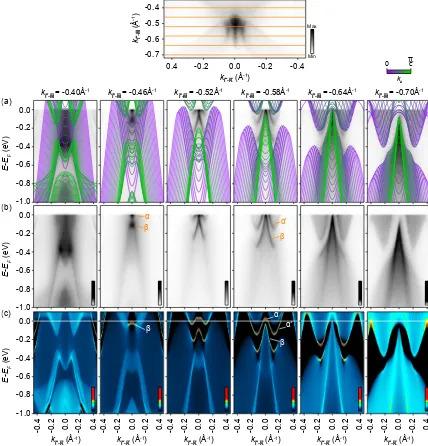
FIG. 1. (a) ARPES Fermi surface of PdTe2 (EF ±5 meV;h⌫= 107 eV; p-pol, probing close to an A-plane alongkz). (b) In-plane dispersion along the M direction (h⌫= 24 eV, probing a similarkz value as in (a)). (c) Corresponding supercell calculations of the dispersion over an extended energy range, projected onto the top two unit cells of PdTe2. (d) Out-of-plane bulk band dispersions along the A direction of the Brillouin zone from DFT calculations, projected onto the chalcogenpx,y (red) andpz(cyan) orbitals. (e-h) Equivalent measurements and calculations for PtSe2 (ARPES measurements:h⌫= 107 eV; p-pol). Topological surface states (TSS), bulk Dirac points (BDP), and inverted band gaps (IBG) are labeled.
functional as implemented in the WIEN2K program [23], using a 20⇥20⇥20k-mesh. To calculate the surface elec-tronic structure, tight binding supercells containing 100 formula units of PdTe2 or PtSe2stacked along the crys-tallinec-direction were constructed from the bulk DFT calculations using maximally localized Wannier functions with chalcogenp-orbitals and transition-metald-orbitals as the projection centres [24–26].
The electronic structure of PdTe2, as well as its sis-ter compound PtSe2, are summarised in Fig. 1. While the Pd/Ptdstates retain a fully-filled configuration, and are thus located well below the Fermi level [27], a con-ducting state is obtained due to an energetic overlap of predominantly Te/Se-derived bonding and anti-bonding states [28]. In PdTe2, this leads to a complex multi-band Fermi surface (Fig. 1(a)). Strong inter-layer interactions for the chalcogen-derived states render this Fermi surface three-dimensional, despite the layered nature of this com-pound. Many of the observed spectral features are there-fore di↵use in our measured Fermi surface from ARPES, reflecting the inherent surface sensitivity, and thus poor kzresolution, of photoemission. Similarly broad features, including a recently-identified type-II bulk Dirac cone [29, 30] centered at E EF = 0.65 eV, can also be seen in our measured dispersions (Fig. 1(b)) as well as in our supercell calculations where bulk bands at di↵erent kzvalues are projected onto the surface plane (Fig. 1(c).
A number of much sharper features are also observed. A Dirac cone situated ⇠1.75 eV below the Fermi level is clearly evident in our ARPES. This has recently been identified as a topological surface state in PdTe2 and related compounds [29, 31–34]. This arises from a band inversion that occurs within the Te p-orbital manifold, and is induced by a naturally disparate out-of-plane dispersion of pz and px/y-derived bands along kz (Fig. 1(d)) [29]. This same mechanism drives the formation of both the type-II bulk Dirac cone and a further topological surface state located ⇠1 eV below EF, that is visible in our supercell calculations presented here (Fig. 1(c)) and is clearly resolved experimentally in Ref. [29]. These topological states, however, are too far below the Fermi level to play any role in the superconduc-tivity of this system. On the other hand, our measure-ments (Fig. 1(b), see inset) and calculations (Fig. 1(c)) reveal an additional pair of sharp spectral features which intersect the Fermi level approximately mid-way along the M direction. These have negligible dispersion in the out-of-plane direction (Supplementary Fig. S1 [35]), and we thus assign them as surface states.
[image:2.595.56.545.88.332.2]3
and anti-bonding px/y-derived bands (lower and upper pair, respectively, of the red coloured bands in Fig. 1(d)) as they disperse along thekzdirection. A protected bulk Dirac point and an inverted band gap with non-trivialZ2 topological order are therefore generated above the Fermi level. The inverted band gap aboveEF should give rise to topological surface states. While this band inversion is⇠1 eV above the Fermi level along A, the in-plane bandwidths are large, and the relevant band inversion can be traced to the bulk states in the vicinity of the Fermi level at the time-reversal invariant M-point. Here, the pair exchange arising from the bulk boundary correspon-dence of topological surface states [36, 37] enforces that the dispersion of the topological surface states are pulled down towards the Fermi level. Experimentally, we find that both the “upper” (labeled ↵) and “lower” (labeled ) branch of the topological state cross EF (Fig. 1(b, inset)), although the occupied bandwidth of the↵-band along this direction is small (⇡20 meV).
[image:3.595.307.544.87.419.2]To validate the above picture, we compare PdTe2with its sister compound PtSe2. The occupied electronic structure is similar to PdTe2, hosting a type-II bulk Dirac cone and a pair of topological surface states be-low EF (Fig. 1(f,h)). These arise from the crossing of the Sepz-derived band with the bonding Se px/y bands (Fig. 1(e)) [29, 32]. The bandwidth of the Sepz-derived band is, however, much smaller than that of the Te-derived one owing to the higher electronegativity of Se than Te. This leads to a stronger metal-chalcogen bond, and therefore weaker interlayer hopping in PtSe2. Cru-cially, although a semi-metallic ground state still occurs (Fig. 1(g)), the upper and lower branches of Se-derived states remain completely separable in PtSe2. The band inversions aboveEF that occur for PdTe2 are therefore absent in this compound (Fig. 1(e-h)).
Figure 2 shows the Fermi surfaces formed by the topo-logical states which intersect the Fermi level in the Te-based material. The↵band forms a small approximately circular electron pocket, located approximately midway along M. This electron pocket rapidly shrinks and then vanishes in constant energy slices taken below the Fermi level (Fig. 2(b)), reflecting the narrow occupied bandwidth of this band along M. However, this is only a local minimum of the surface state dispersion lo-cated within a narrow projected bulk band gap along this direction (see Fig. 2(e,f); further cuts are shown in Supplemental Fig. S2 [35]). The band disperses upwards above the Fermi level along the direction perpendicular to M before turning over again to form the intense rim of spectral weight that borders the three-dimensional bulk bands that are evident as di↵use filled-in spectral weight spanning out away from the M line in Fig. 2(b). With increasing momentum away from this line, these surface states become degenerate with the bulk bands, and ulti-mately lose all spectral weight. They thus appear to form open-ended arc-like features. We stress that these are not
M K
Γ
0.0 0.2 0.4
-0.2 -0.4 E-E F (m eV) 0 -20 -40 E-E F (eV) 0.0 -0.2 -0.4 -0.6 0.0 -0.2 -0.4 -0.6 -60 -80 -100 (b) (e) (f) (a) (c) (d) 0.0 0.1
-0.1 -0.1 0.0 0.1 -0.1 0.0 0.1
0 Max -0.7 -0.6 -0.5 -0.4 -0.7 -0.6 -0.5 -0.4 0.2 -0.2 0.0
kΓ-K(Å-1)
0.0 0.2 0.4
-0.2 -0.4
kΓ-K(Å-1)
0.0 0.2 0.4
-0.2 -0.4
kΓ-K(Å-1) kΓ-K(Å-1)
-0.6 -0.5 -0.4 -100 100 0 0 Max Spin pol. (%) Int. Int. 0 0 Max kz π c 0 Max kΓ-M (Å -1) kΓ-M (Å -1) kΓ-M (Å -1) α (e) α' β α α' β α' β
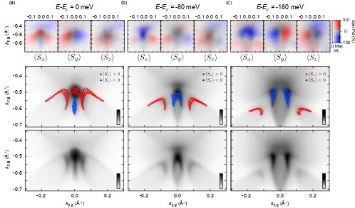
FIG. 2. (a) Three-component spin-resolved ARPES Fermi surface measured (h⌫ = 24eV) over the range shown in (b). HerehSxi andhSyiare perpendicular to and along the M direction, respectively. hSzi is the out-of-plane spin component. (b) Near-EF Constant energy contours mea-sured from spin-integrated ARPES (h⌫ = 24eV) over the portion of the surface Brillouin zone where the topological states reside. (c) Schematic representation of the global Fermi surface spin texture throughout the surface Brillouin zone that is deduced from our measurements. (d) The in-plane spin texture (arrows) determined directly from the resolved measurements and shown atop the measured spin-integrated Fermi surface segment. (e) ARPES-measured dis-persion (h⌫ = 24 eV) and (f) corresponding supercell cal-culation, cutting through the TSS Fermi surfaces along the dashed line indicated in (b). kz-dependent bulk band calcu-lations are overlaid in (e) and visible as di↵use spectral weight in (f), demonstrating how small projected band gaps control the dispersion of the TSS (see also Supplemental Fig. S2 [35]).
The small projected band gaps of the bulk spectrum thus leads to only small momentum space regions cen-tered along the M directions in which the surface states are well defined. This results in a rich multi-valley Fermi surface (Fig. 1(a)), far removed from the generic isolated near-circular Fermi surfaces of topological sur-face states in, e.g., Bi2Se3 class topological insulators. Nonetheless, we show in Fig. 2 that the Fermi surfaces observed here still maintain a spin texture reminiscent of the simple chirality of a conventional topological surface state.
Our spin-ARPES measurements reveal that the sur-face states host a strong spin polarisation (> 70% from fits to energy distribution curves (EDCs); Supplemental Fig. S3 [35]). Along M, the chiralhSxi(perpendicular to M) spin component is dominant (Fig. 2(a)), consis-tent with the underlying trigonal symmetry of the crystal surface. The↵and bands have opposite spin polarisa-tion, supporting their assignment as the two branches of a topological surface state. Both Fermi crossings of the ↵ band along M have the same sign of hSxi. The spin, therefore, does not wind around the closed circu-lar ↵-band Fermi surface. Instead, it develops a finite hSyi(parallel to M) component of opposite sign on the two sides of the high-symmetry M line, cant-ing the spin towards the Brillouin zone boundary in the in-plane direction. Similarly, the two↵0-bands have the same sign ofhSxibut opposite sign ofhSyi, as shown ex-tracted from our experimental spin-polarised Fermi face maps in Fig. 2(d). The overall result is a Fermi sur-face spin-texture of the↵-derived Fermi surfaces that has a global chiral winding around the Brillouin zone centre, but with a significant radial component developing away from the M line (Fig. 2(c)), similar to what might be expected for a more conventional topological surface state if it develops a hexagonal warping away from cir-cular geometry [47, 48]. While at the Fermi level only the chiral component of the -band is visible, similar ra-dial components, as well as an out-of-plane spin canting, develop for its highly-fragmented surface state contours belowEF (Supplemental Fig. S4 [35]).
These findings raise an exciting prospect to investi-gate how such topological states, with their complex Fermi surface spin textures, interplay with the bulk su-perconductivity of PdTe2. To this end, we investigate the superconductivity at the surface using low-temperature STM (Fig. 3). Our measured tunneling spectra at 8 K (Fig. 3(b)) reveal two pronounced peaks in the local den-sity of states centered at approximately -10 meV and -130 meV. These are in excellent agreement with the positions of clear peaks in the density of states arising from the van Hove singularities of the ↵ and TSS bands, evident in our angle-integrated ARPES spectra (Fig. 3(b)). Such features remain in our STS measure-ments upon cooling (Fig. 3(b)), indicating the persistence of the Fermi-level TSSs observed here into the
supercon-0.0 0.4 0.8 1.2 0.0 0.0 -0.8
-200 -100 0 100
-0.4 0.4 0.8
0.5 1.0 1.5 2.0 2.5 3.0 NS SS Normalised dI/dV dI/dV ,Intensity (arb. u.) Bias (mV) (b) (c) (d) (e) Normalised ZBC0.08 0.06 0.04 0.02 0.1 0.3 0.5 Bias (mV)
E-EF(meV), Bias (mV) R(nm) 0.0 -0.4 -0.8 0.4 0 50 225nm 0.10
100 150 200
0.0 2.0 1.0 ARPES 5K STM 8K STM 40mK (nm) (pm) 0 0 2 4 6 8
2 4 6 8
(a) 0 -60 60 α β TSS:
FIG. 3. (a) Surface topography of PdTe2 measured atT = 8 K from a 8.5⇥8.5 nm2 region (Bias voltage: V = 10 mV, Tunneling current set-point: I= 0.4 nA). (b) ARPES spectra (top;T= 5 K,h⌫= 24 eV, integrated along the M direc-tion of the Brillouin zone) and di↵erential conductance spec-tra measured using STM atT= 8 K (middle) andT= 40 mK (bottom). (c) Low-energy spectra measured at 40 mK and performed with a normal (N, top) and superconducting (S, bottom) tip. The NS-junction (SS-junction) spectra are av-eraged over a 5.4 x 5.4 nm2 (10⇥10 nm2) area and are nor-malised to the conductance at 0.6 mV. The dashed lines show the result of Dynes fits, incorporating thermal broadening of 100 mK [21]. For the NS-junction, a lock-in amplitude of 25µV was used, with the fit yielding a sample superconduct-ing gap size of = 215µV with a Dynes broadening parame-ter of = 65µV. For the SS-junction, a lock-in amplitude of 30µV was used with Dynes broadenings of 18 µV and 4µV for sample and tip respectively. The obtained superconduct-ing gap of the sample and tip is 240µV. (d) Radially averaged decay of zero bias conductance (ZBC) with distance (R) from the centre of a vortex core, measured with a superconduct-ing tip in a magnetic field of 7±2 mT. The inset shows the real-space image of the vortex via its enhanced ZBC. (e) The radial dependence of the full superconducting gap structure with distance from the centre of the vortex core, obtained using V=8 mV, I=0.4 nA and a lock in amplitude of 30µV.
[image:4.595.307.547.79.331.2]su-5
perconducting gap. Crucially, however, there is no evi-dence of nodes in the superconducting order parameter or of in-gap states. Similar conclusions can be drawn from measurements performed using a superconducting tip (Fig. 3(c)), where again a clear lack of any zero-energy bound states is evident.
Measuring the collapse of the superconducting gap in a magnetic field applied normal to the sample surface (see Supplemental Fig. 5 [35] for a detailed description), we estimate an upper critical field,H?
c2 ⇡20 mT. This is consistent with the upper critical field of the bulk su-perconducting state as judged from susceptibility mea-surements [49]. Intriguingly, the bulk superconductiv-ity in PdTe2 has recently been reported to be of type I character [49]. We have, however, observed a vortex core in our STM measurements in a magnetic field of 7±2 mT (Fig. 3(d)), indicating that the superconductiv-ity we probe is of type-II character.
From the measured decay length of the vortex core of 175±67 nm (Fig. 3(d)), this would suggest an upper crit-ical field ofHc2⇡11 mT for a BCS superconductor, as-suming a one-to-one correspondence of the measured de-cay length to the coherence length. This is in reasonable agreement with our measured value of the surface upper critical field. Finally, we note that scanning tunneling spectroscopy performed as a function of distance away from the centre of the vortex core (Fig. 3(e)) again yields no evidence for the presence of zero-energy bound states. Taken together, these results demonstrate that the sur-face of PdTe2 supports a conventional fully-gapped s -wave superconducting state, well described by BCS the-ory. This co-exists with well-defined topologically non-trivial surface states, with complex multi-component and multi-valley Fermi surfaces and rich vorticial spin tex-tures.
The complexity of the surface Fermi surface, as well as the presence of numerous bulk states degenerate in en-ergy but at di↵erent in-plane momenta, may ultimately explain why the dominant superconducting pairing re-mains topologically trivial at the surface. In any case, our results clearly demonstrate that the presence of topo-logically non-trivial states at the Fermi level is not a sufficient criterion to realise topological superconductiv-ity. Beyond this, our findings highlight the importance of kz-dependent band inversions within a single orbital manifold for generating topological surface states with rich and complex surface Fermi surfaces. Moreover, they demonstrate how these can be e↵ectively tuned by vary-ing interlayer hoppvary-ing strengths, pavvary-ing the way to the design of new topological materials.
Acknowledgements: We gratefully acknowledge sup-port from the Leverhulme Trust, the Engineering and Physical Sciences Research Council, UK (Grant Nos. EP/M023427/1 and EP/I031014/1), the Royal Society, CREST, JST (Nos. JPMJCR16F1 and
JP-MJCR16F2), the Japan Society for Promotion of Science (Grant-in-Aid for Scientific Research (S); No. 24224009 and (B); No. 16H03847), and the International Max-Planck Partnership for Measurement and Observation at the Quantum Limit. This work has been partly per-formed in the framework of the nanoscience foundry and fine analysis (NFFA-MIUR Italy, Progetti Internazion-ali) facility. OJC, MJN, LB, VS, and JMR acknowl-edge EPSRC for PhD studentship support through grant Nos. EP/K503162/1, EP/G03673X/1, EP/L505079/1, and EP/L015110/1. IM acknowledges PhD studentship support from the IMPRS for the Chemistry and Physics of Quantum Materials. We thank Diamond Light Source (via Proposal Nos. SI9500, SI12469, SI13438, and SI16262) and Elettra synchrotron for access to the I05 and APE beamlines, respectively, that contributed to the results presented here. The data that underpins the find-ings of this study are available at http://dx.doi.org/xxxx.
⇤ gpw2@st-andrews.ac.uk
† bahramy@ap.t.u-tokyo.ac.jp ‡ philip.king@st-andrews.ac.uk
[1] Read, N. & Green, D. Paired states of fermions in two di-mensions with breaking of parity and time-reversal sym-metries and the fractional quantum Hall e↵ect. Phys. Rev. B 61, 10267 (2000).
[2] Gor’kov, L. P. and Rashba, E. I. Superconducting 2D System with Lifted Spin Degeneracy: Mixed Singlet-Triplet State. Phys. Rev. Lett.87, 037004 (2001). [3] Schnyder, A. P., Ryu, S, Furusaki, A. and Ludwig, A.
W. W. Classification of topological insulators and super-conductors in three spatial dimensionsPhys. Rev. B 78, 195125 (2008).
[4] Sato, M. and Fujimoto, S. Topological phases of noncen-trosymmetric superconductors: Edge states, Majorana fermions, and non-Abelian statistics Phys. Rev. B 79, 094504 (2009).
[5] Sun, Z.et al.Dirac surface states and nature of supercon-ductivity in Noncentrosymmetric BiPdNature Commun. 6, 6633 (2015).
[6] Sato, M., & Ando, Y. Topological superconductors: a review Rep. Prog. Phys.80,076501 (2017).
[7] Maier, L.et al. Induced Superconductivity in the Three-Dimensional Topological Insulator HgTePhys. Rev. Lett. 109, 186806 (2012).
[8] Deacon, R. S.et al. Josephson Radiation from Gapless Andreev Bound States in HgTe-Based Topological Junc-tions. Phys. Rev. X 7, 021011 (2017).
[9] Yang, F.et al.Proximity-e↵ect-induced superconducting phase in the topological insulator Bi2Se3. Phys. Rev. B. 86, 134504 (2012).
[10] Zareapour, P.et al.Proximity-induced high-temperature superconductivity in the topological insulators Bi2Se3 and Bi2Te3. Nature Commun.3, 1056 (2012).
its Implications for Pairing in the Undoped Topological Insulator Phys. Rev. Lett.104, 057001 (2010).
[13] Matano, K., Kriener, M., Segawa, K.,Ando, Y. and Zheng, G.-q. Spin-rotation symmetry breaking in the superconducting state of CuxBi2Se3 Nature Phys. 12, 852854 (2016).
[14] Levy, N.et al.Experimental Evidence for s-Wave Pairing Symmetry in Superconducting CuxBi2Se3 Single Crys-tals Using a Scanning Tunneling Microscope Phys. Rev. Lett.110, 117001 (2013).
[15] Schneeloch, J. A., Zhong, R. D., Xu, Z. J., Gu, G. D., and Tranquada, J. M. Dependence of superconductivity in CuxBi2Se3on quenching conditions Phys. Rev. B 91, 144506 (2015).
[16] Raub, Ch. J.et al. The occurrence of superconductivity in sulfides, selenides, tellurides of Pt-group metals. J. Phys. and Chem. of Solids 26,12 (1965).
[17] Kjekshus, A. & Pearson, W. B. Constitution and mag-netic and electrical properties of palladium tellurides (PdTe-PdTe2).Can. J. of Phys.43,3 (1965).
[18] Ryu, G. Superconductivity in Cu-Intercalated CdI2 -Type PdTe2 J. Supercond. Nov. Magn.28, 3275-3280 (2015).
[19] Bigi, C. et al. Very efficient spin polarization analysis (VESPA): new exchange scattering-based setup for spin-resolved ARPES at APE-NFFA beamline at Elettra. J. Synchrotron Rad.24,750-756 (2017).
[20] Hoesch, M. et al. A facility for the analysis of the electronic structures of solids and their surfaces by syn-chrotron radiation photoelectron spectroscopy. Rev. Sci. Instr.88,4973562 (2017).
[21] Singh, U. R., Enayat, M., White, S. C., & Wahl, P. Construction and performance of a dilution-refrigerator based spectroscopic-imaging scanning tunneling micro-scope Rev. Sci. Instruments 84, 013708 (2013). [22] White, S. C., Singh, U. R. & Wahl, P. A sti↵
scan-ning tunneling microscopy head for measurement at low temperatures and in high magnetic fields Rev. Sci. In-struments 82, 113708 (2011).
[23] Balaha, P.et al.WIEN2K package, Version 13.1 (2013). [24] Souza, I. et al. Maximally localized Wannier functions for entangled energy bands. Phys. Rev. B. 65, 035109 (2001).
[25] Mostofi, A. A.et al.Wannier90: a tool for obtaining max-imally localized Wannier functions. Comp. Phys. Com-mun.178,685-699 (2008).
[26] Kunes, J. et al. WIEN2WANNIER: from linearized augmented plane waves to maximally localized Wan-nier functions. Comp. Phys. Commun. 181,1888-1895 (2010).
[27] Chhowalla, M.et al. The chemistry of two-dimensional layered transition metal dichalcogenide nanosheets. Na-ture Chemistry 5,263-275 (2013).
[28] Furuseth, S. et al. Redetermined Crystal Structures of NiTe2, PdTe2, PtS2, and PtTe2. Acta Chemica Scandi-navica 19,257-258 (1958).
[29] Bahramy, M. S., Clark, O. J.et al. Ubiquitous formation of bulk Dirac cones and topological surface states from a single orbital manifold in transition-metal dichalco-genides. Nature Mater.17,21-28 (2018).
[30] Noh, H.-J. et al. Experimental Realization of Type-II Dirac Fermions in a PdTe2 Superconductor. Phys. Rev. Lett.119,016401 (2017).
[31] Yan, L.et al. Identification of Topological Surface State in PdTe2 Superconductor by Angle-Resolved Photoe-mission Spectroscopy. Chinese Phys. Lett. 32, 067303 (2015).
[32] Huang, H., Zhou, S., Duan, W. Type-II Dirac fermions in the PtSe2class of transition metal dichalcogenides.Phys. Rev. B.94,121117(R) (2016).
[33] Zhang, K.,et al.Experimental evidence for type-II Dirac semimetal in PtSe2 Phys. Rev. B.96,125102 (2017). [34] Yan, M.et al.Lorentz-violating type-II Dirac fermions in
transition metal dichalcogenide PtTe2 Nature Commun. 8,257 (2017).
[35] see Supplemental materials
[36] Bahramy, M.S.et al.Emergent quantum confinement at topological insulator surfaces. Nature Commun.3, 1159 (2012).
[37] Wray, L.A. et al. A topological insulator surface under strong Coulomb, magnetic and disorder perturbations. Nature Phys.7, 32 (2011).
[38] Young, S. M. et al. Dirac Semimetal in Three Dimen-sions. Phys. Rev. Lett.108,140405 (2012)
[39] Borisenko, S.et al.Experimental Realization of a Three-Dimensional Dirac Semimetal. Phys. Rev. Lett 113, 027603 (2014).
[40] Liu, Z. K.et al.Discovery of a Three-Dimensional Topo-logical Dirac Semimetal, Na3Bi. Science 343, 864-867 (2014).
[41] Wan, X.et al. Topological semimetal and Fermi-arc sur-face states in the electronic structure of pyrochlore iri-dates. Phys. Rev. B 83,205101 (2011).
[42] Xu, S.-Y.et al. Discovery of a Weyl fermion semimetal and topological Fermi arcs.Science349,613-617 (2015). [43] Lv, B. Q. et al. Observation of Weyl nodes in TaAs.
Nature Phys.11,724-727 (2015).
[44] Huang, L. et al. Spectroscopic evidence for a type II Weyl semimetallic state in MoTe2. Nature Mater. 15, 1155-1160 (2016).
[45] Soluyanov, A. A.et al.Type-II Weyl semimetals.Nature 527,495-498 (2015).
[46] McCormick, T. M., Kimchi, I. and Trivedi, N. Minimal models for topological Weyl semimetals. Phys. Rev. B 95,075133 (2017).
[47] Fu, L. Hexagonal Warping E↵ects in the Surface States of the Topological Insulator Bi2Te3. Phys. Rev. Lett.103, 266801 (2009).
[48] Michiardi, M.et al.Strongly anisotropic spin-orbit split-ting in a two-dimensional electron gas.Phys. Rev. B91, 035445 (2015)
Supplemental Materials
Fermiology and superconductivity of topological surface states in PdTe
2O. J. Clark,1 M. J. Neat,1 K. Okawa,2 L. Bawden,1 I. Markovi´c,1, 3 F. Mazzola,1
J. Feng,1, 4 V. Sunko,1, 3 J. M. Riley,1, 5 W. Meevasana,6, 7 J. Fujii,8 I. Vobornik,8
T. K. Kim,5 M. Hoesch,5 T. Sasagawa,2 P. Wahl,1 M. S. Bahramy,9, 10 and P. D. C. King1
1SUPA, School of Physics and Astronomy, University of St. Andrews, St. Andrews KY16 9SS, United Kingdom
2Materials and Structures Laboratory, Tokyo Institute of Technology, Kanagawa 226-8503, Japan 3Max Planck Institute for Chemical Physics of Solids, N¨othnitzer Straße 40, 01187 Dresden, Germany
4Suzhou Institute of Nano-Tech. and Nanobionics (SINANO),
CAS, 398 Ruoshui Road, SEID, SIP, Suzhou, 215123, China
5Diamond Light Source, Harwell Campus, Didcot, OX11 0DE, United Kingdom 6School of Physics, Suranaree University of Technology, Nakhon Ratchasima, 30000, Thailand
7NANOTEC-SUT Center of Excellence on Advanced Functional Nanomaterials,
Suranaree University of Technology, Nakhon Ratchasima 30000, Thailand 8Istituto Officina dei Materiali (IOM)-CNR, Laboratorio TASC,
in Area Science Park, S.S.14, Km 163.5, I-34149 Trieste, Italy 9Quantum-Phase Electronics Center and Department of Applied Physics,
The University of Tokyo, Tokyo 113-8656, Japan
10RIKEN center for Emergent Matter Science (CEMS), Wako 351-0198, Japan
Photon energy-dependent ARPES
To verify the dimensionality of both surface and bulk states in PdTe2and PtSe2, we show in Supplemental Fig. S1 kz dispersions of both compounds obtained from photon-energy dependent ARPES. To determine the out-of-plane momentum probed, we employ a free electron final state model
kz= 1
~ p
2me(V0+Ekcos2✓), (1)
where✓is the in-plane emission angle,Ek is the photo-electron kinetic energy andV0is the inner potential. We find best agreement to density-functional theory calculations taking a c-axis lattice constant of 5.13 ˚A 1 (5.09 ˚A 1) for PdTe2 (PtSe2) and an inner potential of 16 eV for both compounds.
The states labeled as TSS in PdTe2do not disperse with changing photon energy (i.e., they have nokzdispersion), consistent with their assignment as topological surface states. Conversely, the conduction band in PtSe2 shows significant dispersion, hence demonstrating the three-dimensional bulk nature of this electron pocket at the Fermi level.
(d) (b)
TSS
kΓ-M(Å-1)
0.0 0.5 -0.5
kΓ-M(Å-1)
0.0 0.5 -0.5
3.0 -3.0
-2.5 -2.0 -1.5 -1.0 -0.5 0.0
-3.5
3.5 4.0 4.5 5.0 5.5
kz(Å-1) kz=
E-E
F
(eV)
(a) (b)
(c) (d)
-1.0 -0.5 0.0
E-E
F
(eV)
3.0 3.5 4.0 4.5 5.0 5.5
kz(Å-1)
bulk
kz=
1T
-PdT
e2
1T
-PtSe
2
FIG. S1. (a) Measured dispersion of PdTe2 along M. The vertical line indicates the selected energy-distribution curve
[image:8.595.130.471.294.592.2]3
Detailed band dispersion of Fermi-level topological surface states
Supplemental Fig. S2 clarifies how the topological surface states, appearing as sharp features in our measured spectra, emerge out of the bulk band continuum. The three-dimensional bulk bands are visible in our ARPES as di↵use spectral weight (Supplemental Fig. S2(b)), due to the surface-sensitivity, and hence poorkz-resolution, of ARPES. Overlaid
kz-dependent bulk DFT calculations (Supplemental Fig. S2(a)) confirm how the surface states are well defined and
clearly resolved only in the projected bulk band gaps. Thus, the projected bulk band gaps can be considered to shape the dispersions of the surface states, even causing the upwards dispersion of the↵ band very close to the Brillouin
zone centre to turn over and disperse back below the Fermi level, before it disperses upwards again to form the↵0
bands as evident in our surface supercell calculations shown in Supplemental Fig. S2(c).
(a) kΓ-M= -0.40Å
-1 k
Γ-M= -0.46Å-1 kΓ-M= -0.52Å-1
kΓ-M
(Å
-1)
kΓ-M= -0.58Å-1 k
Γ-M= -0.64Å-1 kΓ-M= -0.70Å-1
E-E
F
(eV)
0.0
-0.2
-0.4
-0.6
-0.8
-1.0 (b)
E-E
F
(eV)
0.0
-0.2
-0.4
-0.6
-0.8
-1.0 (c)
E-E
F
(eV)
0.0
-0.2
-0.4
-0.6
-0.8
0.0 0.4
-0.4 -0.2 -0.2 kΓ-K(Å-1)
0.0 0.4
-0.4 -0.2 -0.2 kΓ-K(Å-1)
0.0 0.4
-0.4 -0.2 -0.2 kΓ-K(Å-1)
0.0
0.4 -0.4
Min Max -0.4
-0.5 -0.6
-0.7
-0.2 -0.2
kΓ-K(Å-1)
0.0 0.4
-0.4 -0.2 -0.2 kΓ-K(Å-1)
0.0 0.4
-0.4 -0.2 -0.2 kΓ-K(Å-1)
0.0 0.4
-0.4 -0.2 -0.2 kΓ-K(Å-1) -1.0
β
α α' β
β α'
α
β
0
kz
π c
[image:9.595.83.511.216.662.2]Spin-resolved ARPES of PdTe2
To confirm the spin textures evident in the spin-resolved Fermi surface maps shown in Fig. 2(a) of the main text, we also performed a series of resolved energy distribution curves, as shown in Supplemental Fig. S3. The spin-resolved EDCs were determined as
Ii",#= Itot
i (1±Pi)
2 . (2)
wherei={x, y, z},Ii",#is the spin-resolved intensity,Pi is the spin polarisation, calculated as
Pi= I
+
i Ii S(Itot
i )
, (3)
S is the relevant Sherman function for the detector in use, andItot
i =Ii++Ii whereIi± is the measured intensity profile for a positively or negatively magnetised detector, corrected by a relative efficiency calibration determined from the portions of the EDCs corresponding to unpolarised di↵use background intensity. Multiple VLEED targets were used through the course of this study, with Sherman functions determined to be betweenS= 0.2 andS= 0.43 from comparison measurements on the Rashba-split surface states of Au(111). The signs and magnitudes of all spin polarisations evident from these EDCs are in good agreement with the spin-resolved Fermi surface shown in Fig. 2 of the main text as well as spin-resolved constant energy contours at higher binding energy shown in Supplemental Fig. S4.
This measurement mode also facilites more quantitative analysis. For this, the raw EDCs (i.e., before correcting for the Sherman function) were fit to Lorentzian peaks with a Gaussian broadening of 50 meV applied to account for finite experimental resolution. A Fermi-Dirac distribution and a Shirley background were included in this analysis. An example fit to bothI+
x and Ix are shown in Supplemental Fig. S3(d) for the EDC labeledk7. From the ratio of
the areas of the fitted components and the relevant Sherman function ofS= 0.2, these fits yield spin polarizations of +73% and 72% for thehSxicomponent of the upper (↵) and lower ( ) branches of the TSS respectively.
-0.0 -0.4
-0.8 -0.8 -0.4 -0.0
E-EF(eV) -0.0
-0.4 -0.8
E-EF(eV) E-EF(eV)
-0.0 -0.4
-0.8
E-EF(eV) -0.0
-0.4 -0.8
E-EF(eV) -k1
-k2
-k3
-k4
-k5
(b) (c) (d)
Intensity
(arb.
units) k6
k7
k7
k7
k8
k6 k6
k7
k8
Data points Total Fit Peaks Background
Example Fit -0.4
-0.5 -0.6 -0.7
-0.2 -0.0
-0.4 -0.6 -0.8 0.0
-0.2 0.2
0.0 -0.2
-0.7 -0.5 0.2
kΓ-K(Å -1)
kΓ-M(Å -1)
kΓ-K(Å -1)
kΓ-M
(Å
-1)
E-E
F
(eV) k5
k4
k3
k2
k1
(a)
k6 k7
k8
FIG. S3. (a) ARPES Fermi surface over the region of the Fermi-level TSSs (left) and dispersions measured along the orange and green lines (right). Orange and green dots on the Fermi surface and lines in the measured dispersions indicate the positions of spin-EDCs numbered k1 though k8shown in (b) and (c). A negative sign indicates that the measurement was performed at
[image:10.595.98.502.410.662.2]5
For the spin-resolved constant energy slices (Fig. 2 and Supplemental Fig. S4), spin polarisations are determined according to Eqn. 2, where Ii± is corrected by a relative efficiency calibration as determined from spin-resolved
constant energy slices performed atE EF=-8.45 eV where there is only di↵use unpolarised background intensity.
The spin-resolved constant energy slices are then plotted using a two-dimensional colour map to show both the polarisationPiand the total intensityIitot, as shown in the accompanying colour bars. The in-plane vector schematics
shown in Fig. 2(d) and in the middle row of Supplemental Fig. S4 are determined directly from these plots. Arrows are at k-vectors corresponding to the positions of bands from spin-integrated ARPES and are calculated using
Ixtot
q
P2
x+Py2 (4)
for their magnitudes, and
tan 1Py Px
or ⇡+ tan 1Py Px
(5)
for their directions, for positive and negative signs ofPxrespectively.
Supplemental Fig. S4 shows additional spin-resolved (top) and ARPES (bottom) constant energy contours measured at finite binding energy. These indicate how, like for the↵0 bands, the band also opens into seemingly open and disconnected constant energy contours belowEF as the surface states loose spectral weight when they become surface
resonances. They also reveal an increased radial component of the spin texture as well as an enhanced out-of-plane spin canting of the band developing belowEF.
(a)
0.0 0.1
-0.1 -0.10.0 0.1 -0.10.0 0.1 -0.10.0 0.1 -0.10.0 0.1 -0.10.0 0.1 -0.10.0 0.1 -0.10.0 0.1 -0.10.0 0.1
(b) (c)
-0.7 -0.6 -0.5 -0.4
kΓ-M
(Å
-1)
-0.7 -0.6 -0.5 -0.4 -0.6 -0.5 -0.4
kΓ-M
(Å
-1)
kΓ-M
(Å
-1)
0.2 -0.2 0.0
kΓ-K(Å-1)
0.2 -0.2 0.0
kΓ-K(Å-1)
0.2 -0.2 0.0
kΓ-K(Å-1)
E-EF=0 meV E-EF=-80 meV E-EF=-180 meV
-100 100
0
0 Max Int.
Spin
Pol
[image:11.595.47.545.346.639.2](%)
FIG. S4. Three-component spin-resolved constant energy contours (top row) at (a)E EF = 0, (b) 80 and (c) 180 meV.
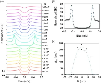
DeterminingHc2 from magnetic field dependent STM measurements
Hc2is determined from the magnetic field-dependence of the sample superconducting gap (Supplemental Fig. S5(a),
as determined from BCS-Dynes model fits to spectra measured using a superconducting tip (Supplemental Fig. S5(b)). The magnetic field-dependent gap was fit according to
(H) = (0)⇣1 ⇣H
Hc ⌘2⌘
, (6)
where (H) and (0) are the gap sizes in a magnetic field applied normal to the sample surface, H, and in zero
field, respectively. The superconducting tip gap was assumed to be constant at 240µV. This analysis results inHc2
of 18±5 mT, as shown in Supplemental Fig. S5(c). All applied field values are stated after calibration using ain situ
Hall probe. The error is approximately±2 mT.
Bias (mV) H(mT)
0.0 0.4 0.8
-0.4 -0.8 0.0 1.0
H
(a) (b)
(c)
0.0
0.0
-0.8 -0.4 0.4 0.8
0.5 1.0 1.5 2.0 2.5 3.0
Bias (mV)
ΔSC
(μeV)
0 0
50 100 150 200 250
-10 -20
-30 10 20 30
Normalised
ZBC Normalised
ZBC
-47 mT -42 mT -37 mT -35 mT -28 mT -18 mT -14 mT -10 mT -8 mT 0 mT 4 mT 0 mT 8 mT 16 mT 18 mT 18 mT 41 mT 92 mT 189 mT 471 mT 965 mT
[image:12.595.127.472.262.545.2]

![Fig. S3 [35]). Along ��M, the chiral hSxi (perpendicularto ��M) spin component is dominant (Fig](https://thumb-us.123doks.com/thumbv2/123dok_us/8715807.383839/4.595.307.547.79.331/fig-chiral-hsxi-perpendicularto-spin-component-dominant-fig.webp)