A Thesis Submitted for the Degree of MPhil at the
University of St. Andrews
2011
Full metadata for this item is available in Research@StAndrews:FullText
at:
http://research-repository.st-andrews.ac.uk/
Please use this identifier to cite or link to this item: http://hdl.handle.net/10023/2532
Silicon Electro-optic Modulator
Fengqiao Dong
This thesis is submitted in partial fulfilment for the
degree of MPhil
at the
University of St Andrews
ii
length, has been written by me, that it is the record of work carried out by me and that it has not been submitted in any previous application for a higher degree.
I was admitted as a research student in September, 2007 and as a candidate for the degree of MPhil in September, 2007; the higher study for which this is a record was carried out in the University of St Andrews between 2007 and 2011.
Date ………… signature of candidate ………
2. Supervisor’s declaration:
I hereby certify that the candidate has fulfilled the conditions of the Resolution and Regulations appropriate for the degree of MPhil in the University of St Andrews and that the candidate is qualified to submit this thesis in application for that degree.
Date ………… signature of supervisor ………
3. Permission for electronic publication:
In submitting this thesis to the University of St Andrews I understand that I am giving permission for it to be made available for use in accordance with the regulations of the University Library for the time being in force, subject to any copyright vested in the work not being affected thereby. I also understand that the title and the abstract will be published, and that a copy of the work may be made and supplied to any bona fide library or research worker, that my thesis will be electronically accessible for personal or research use unless exempt by award of an embargo as requested below, and that the library has the right to migrate my thesis into new electronic forms as required to ensure continued access to the thesis. I have obtained any third-party copyright permissions that may be required in order to allow such access and migration, or have requested the appropriate embargo below.
The following is an agreed request by candidate and supervisor regarding the electronic publication of this thesis:
Access to printed copy and electronic publication of thesis through the University of St Andrews.
iv
I would like to thank my supervisor, Prof. Thomas F. Krauss, who has guided
me and helped me as much as he could during my study in St Andrews.
I also would like to thank Dr. William Whelan-Curtin (also known as Dr. Liam
O'Faolain), Dr. Juntao Li and Dr. Timothy D. James for the knowledge they have
shared with me and many useful discussions we have made. My special thanks to Dr.
Timothy D. James for proof reading this thesis. I sincerely appreciate all the time
they have spent on this work. I thank Mr Steven Balfour for keeping the cleanroom
in order.
Finally, I would say without the help from the members of the group, it would
be impossible for me to complete this project. They have made the research so
vi
In recent years, as on-chip data transmission has increased dramatically,
much time and effort has been devoted to the development of compact
electro-optic modulators with large bandwidth and low power consumption, which is the
key component for on-chip data links. Silicon which has been widely used in
electronic industry has been considered as a promising material for electro-optic
modulators, due to its mature manufacturing technology and low cost.
In this work, a silicon electro-optic modulator based on a new type of phase
shifter is proposed. The phase shifter is in one arm of an asymmetric Mach-Zehnder
interferometer (MZI) structure and operates very similar to a MOS capacitor. Indium
tin oxide (ITO) is used as an electrode and flowable oxide (FOx, spin-on-glass) is used
as a gate oxide. ITO is being widely used in many electro-optic applications as a
transparent conductor, as it offers both electrical conductivity and optical
transparency, although it has seen less use in optical waveguide devices.
Electrical simulations have been completed in order to study the electrical
performance of the phase shifter and also to improve the design. SiO2 has been used
as a gate oxide in the simulation. The depletion region width and
capacitance-voltage (C-V) characterization have been modelled. Based on the theoretical analysis
and simulation results, n-type silicon with the doping concentration of 1×1017 cm-3
vii
best result. The sheet resistance is around 750 Ω/□ and the optical transmittance is
about 87%.
Aluminium (Al) electrical contacts to silicon have been fabricated and tested.
The HF cleaning and post thermal annealing effect on the contact resistance has
been investigated. The transmission line method (TLM) has been used to determine
the contact resistance. The Al contact resistance is about 335 Ω on n-type silicon
substrate with a doping concentration of 1×1017 cm-3.
ITO-FOx phase shifters and modulators have been fabricated and tested. The
MZI structure of the modulator shows the typical interference pattern. This is
important for realising phase-intensity modulation. Al-FOx phase shifters have also
been fabricated and tested. The transmission depends on the Voltage, both in terms
of phase and the optical loss, clearly indicating a change in carrier density. Although
ITO-FOx phase shifters and modulators did not work successfully due to high optical
losses caused by waveguides sidewall roughness and fabrication process, ITO
showed promise to use in electro-optic modulators as a transparent conducting layer.
The ITO layer separates silicon waveguides from Al contacts and lowers optical losses
due to metal absorption.
Overall, successful operation of a MOS-capacitor type optical phase shifter
has been achieved, but the modulation efficiency is low (1 dB at 50 V) and the
viii
Declarations. . . .ii
Acknowledgement . . . iv
Abstract . . . .vi
Table of contents . . . viii
List of Figures . . . .xii
List of Tables . . . xvi
Chapter 1 Introduction & theory . . . 1
1.1Silicon electro-optic modulator overview . . . 1
1.2Mach-Zehnder interferometric modulation structure . . . 5
1.3Phase shift mechanism . . . 9
1.3.1 Free carrier plasma dispersion effect . . . .10
1.3.2 MOS capacitor phase shifter . . . 15
1.3.3 PN junction phase shifter . . . 17
1.4Slow light photonic crystal waveguide . . . 21
1.5Different types of silicon modulators . . . 26
1.5.1 Modulator based on MOS capacitor . . . 26
1.5.2 Modulator based on carrier depletion PN junction . . . 28
1.5.3 Modulator based on forward biased PIN junction . . . 30
1.5.4 Modulator based on micro-ring resonator . . . 31
1.5.5 Thermo-optic modulator with slow light PhC waveguides . . . 33
1.6Summary & layout of this thesis . . . 35
Chapter 2 Electrical simulation & design . . . 37
ix
2.2.4 Simulation results and discussion . . . 53
2.3Conclusion . . . 58
Chapter 3 Transparent conducting oxide, ITO fabrication & transmittance characterization . . . 61
3.1Transparent conducting oxide. . . 61
3.2ITO properties . . . 63
3.3ITO fabrication . . . 65
3.4ITO optical loss test . . . 67
3.4.1 ITO annealing-transmittance characterization & sheet resistance measurement . . . 67
3.4.2 ITO absorption loss on blank waveguide test . . . 74
3.5Discussion & conclusion. . . 76
Chapter 4 Aluminium-silicon contact characterization . . . .79
4.1Aluminium contact fabrication . . . 79
4.1.1 Aluminium-silicon contact . . . 79
4.1.2 Fabrication process . . . 81
4.2TLM measurement & result . . . 82
4.3Conclusion . . . 88
Chapter 5 Silicon electro-optic modulator fabrication & characterization . . . 91
5.1Silicon electro-optic modulator fabrication . . . 91
5.2Silicon electro-optic modulator optical transmission characterization . . . .101
5.2.1 Asymmetric MZI modulator with ITO on one arm . . . .101
5.2.1.1Absorption due to ITO . . . .104
x
applied voltage . . . 109
5.2.2 Asymmetric MZI modulator with ITO on both arms . . . 112
5.2.2.1Transmission measurement before Fox etching and Al contact fabrication . . . 112
5.2.2.2Transmission measurement after Fox etching and Al contact fabrication . . . 115
5.2.3 Al-Fox phase shifter . . . 120
5.3Discussion & conclusion . . . 124
Chapter 6 Conclusion and future work. . . 127
Appendix . . . 133
xii
Table Description Page
1.1 Mach-Zehnder interferometer 5
1.2 Asymmetric MZI structure for phase-intensity modulation 6
1.3 Asymmetric MZI with phase shifter for phase-intensity modulation 9
1.4 Free carrier plasma effect 13
1.5 Free carriers in n-type MOS capacitor under equilibrium,
depletion and accumulation conditions 16
1.6 Schematic diagram of a PN phase shifter 20
1.7 The depletion region change of a PN junction
before and after applying the voltage 20
1.8 2D and 3D [33] photonic crystals 22
1.9 Illustration of slow light mechanism in
photonic crystal waveguides [38] 23
1.10 Dispersion (ω-k) diagram showing the slow light enhancement 24
1.11 Transmission spectra of slow light engineered
photonic crystal waveguides [41] 25
1.12 Schematic diagram showing the cross-sectional view of
a MOS capacitor waveguide phase shifter on SOI wafer [26] 27
1.13 Cross-sectional view of a reverse biased PN phase shifter [42] 29
1.14 PIN phase shifter with silicon photonic crystal waveguide [44] 31
1.15 Micro-ring resonant electro-optic modulator [45] 32
1.16 Thermo-optic modulator with slow light PhC waveguides [57] 34
2.1 Schematic diagram of phase shifter with no voltage applied 38
[image:16.595.87.509.131.788.2]xiii
2.5 Schematic diagram of the simulated phase shifter 53
2.6 Electric field distribution of the simulated device 54
2.7 Hole density distribution in the MOS Capacitor at +25 V 55
2.8 Electron density distribution in the MOS Capacitor at +25 V 56
2.9 Simulation result of C-V characterization of the MOS capacitor 57
3.1 Potential distribution in Al/SiO2/Si and Al/TE/SiO2/Si structures 62
3.2 Cross-sectional view of the silicon MOS capacitor phase shifter
with transparent conducting oxide (TCO) 62
3.3 45˚ ITO evaporation 66
3.4 Transmittance measurement of the ITO film on a glass slide 68
3.5 ITO transmittance dependence on wavelength 70
3.6 Second transmittance measurement test of 140 nm ITO film
on glass sample 71
3.7 Third transmittance measurement test of 140 nm ITO film
on glass sample 71
3.8 ITO on blank waveguide transmission measurement 75
4.1 TLM measurement 80
4.2 SEM images showing the holes caused by Al spiking silicon 82
4.3 Al contact pads on silicon substrate for TLM measurement 83
4.4 I-V characterization of n-type 1×1017 cm-3 sample
before (a) and after (b) annealing, no HF cleaning 84
4.5 Resistance – spacing characterization of n-type 1×1017 cm-3
xiv
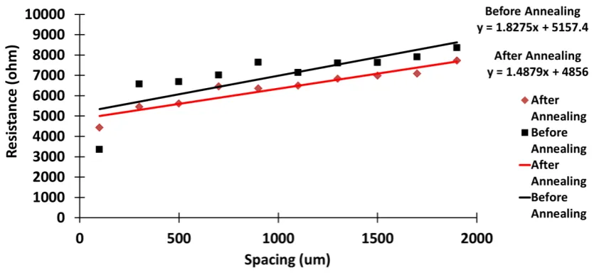
before (a) and after (b) annealing, with HF cleaning 87
4.7 Resistance – spacing characterization of n-type 1×1017 cm-3
sample before and after annealing, with HF cleaning 88
5.1 SOI wafer structure 92
5.2 Silicon photonic crystal fabrication process 93-94
5.3 SEM picture of optical structures after RIE 95
5.4 ITO deposition and lift-off process 97-98
5.5 GDS design structure of an asymmetric MZI 98
5.6 Metal contact lift-off process 99-100
5.7 Asymmetric MZI silicon electro-optic modulators with
ITO only on one arm 102
5.8 Optical transmission spectrum measurement system 103
5.9 Normalised transmission spectra of PhC waveguides
with and without 125 um Long ITO 105-106
5.10 Normalised transmission spectra of MZI modulators
and phase shifters 107-108
5.11 Normalised transmission spectra of PhC400 & PhC410
phase shifters with 50 um ITO at applied voltages 109-111
5.12 Top view of fabricated modulators before Al contact deposition 113
5.13 Normalised transmission spectra with MZI Interference Pattern 114
5.14 Microscope view of fabricated modulators after FOx
etching and Al contact fabrication 116
5.15 Individual PhC waveguides (PhC410) transmission spectra
before and after FOx etching and Al contact fabrication 117
xv
voltagesshowing loss change (over 1 dB) and spectra pattern shift 122-123
6.1 Cross-sectional view of the silicon MOS capacitor phase shifter
xvi
Table Description Page
2.1 Theoretical analysis for typical doping concentrations of n-type
silicon as phase shifter substrate 47
2.2 Theoretically calculated and simulated depletion region width
of a silicon PN junction 51
3.1 Theoretically calculated capacitance of the MOS capacitor phase
shifter in two different structures 64
3.2 Annealing-transmittance-sheet resistance measurement results
of ITO film on a glass slide 69
4.1 Contact resistance with and without HF Clean,
1 | P a g e
Chapter 1
Introduction & Theory
Silicon electro-optic modulator overview
The demand for large data transmission is continuing to increase
exponentially. Network interconnects, for both conventional data networks and
inter-chip data links, continue to scale in complexity and bandwidth year after year
[1]. Because transistors are getting smaller and more compact, the resistance of
copper interconnects and transmission delays increases dramatically when copper
wires decrease to sub 90 nm dimensions [2]. Besides, the power consumption
increases with the data transmission speed in copper interconnects. In order to meet
this increasing demand and tackle the problem with copper, photonic devices have
been introduced into telecommunication and on-chip data links for high speed
2 | P a g e
Although electro-optic modulators based on LiNbO3 and III-V semiconductor
compounds have already been commercially available at speeds up to 40 Gb/s,
silicon electro-optic modulators show more promise in terms of future integration
with silicon electronics in a cost-effective manner. The state-of-the-art silicon
electro-optic modulator is based on a MZI interferometer with a reverse biased PN
junction in both of the arms, achieving a high speed of 40 Gb/s with 20 dB extinction
ratio and an insertion loss of 7 dB. The length of this device is over 1 mm. In order to
have small RC constant, traveling-wave electrodes which allow electrical and optical
signal co-propagation along the waveguide and therefore keep the RF attenuation
low have been used in the modulator [42].
The three critical issues in silicon electro-optic modulator research are RC
time constant, optical insertion loss and size of the device. RC time constant
ultimately limits the modulation speed and can be lowered by designing the device
with smaller capacitance and resistance [42]. Insertion loss limits the optical
performance of the modulator. It can be reduced by using silicon waveguides with
low doping concentrations to lower the free carrier absorption loss. Also, a layer of
transparent conducting material can be used to keep metal contacts away from
silicon waveguides so as to reduce the optical losses due to metal absorption [26].
The size of the device relates to integration with other devices and also cost.
Enhancement techniques such as slow light photonic crystal (PhC) waveguides and
3 | P a g e
similar performance to the state-of-the-art silicon electro-optic modulator with a
shorter length (<100 um) by using slow light PhC waveguides. The electrical
performance, especially the depletion region width and capacitance, has been
investigated and simulated. ITO as a transparent conducting oxide has been
investigated. And the optical loss due to the ITO film has been measured.
Although ruling the electronic industry for decades, silicon was not widely
used in photonic devices initially, due to its own limitations, which includes high
propagation losses (because of scattering induced by waveguide sidewall roughness),
low electro-optic coefficient, low light-emission efficiency, and high
fibre-to-waveguide coupling losses [9]. However, silicon has some excellent material
properties that are important for photonic devices, that have now been recognised
and studied, such as high thermal conductivity, high optical damage threshold, and
high third-order optical nonlinearities [10]. Moreover, light absorption in silicon
waveguides can be neglected, which means silicon is a transparent medium to guide
light [11]. Another important reason of using silicon in photonic devices is that these
devices are highly compatible with mature CMOS manufacturing technology, which
can greatly reduce the cost compared with the devices based on other photonic
materials [12]. At the same time, silicon is a good platform for ultra-compact
monolithic integration of both electronic and photonic components [13]. These
advantages have attracted much effort on developing silicon photonic devices. The
origins of silicon photonics can be traced back to the fundamental works of Soref and
Petermann et al. more than twenty years ago [14-18]. With the progress of
4 | P a g e
Low-loss silicon photonic waveguides with propagation losses down to 1 dB/cm [24]
and even lower ~0.3 dB/cm [25] have been demonstrated. Silicon electro-optic
modulators, as one of the key components for optical interconnects and photonic
integrated circuits (PICs), have also been developed with compact size, high
modulation speed and small power consumption [26-28, 42-45, 47].
In order to realize optical intensity modulation, silicon electro-optic
modulators could be either based on the absorption mechanism or the phase shift
mechanism. As silicon itself is transparent at the telecommunication wavelengths,
absorption based modulators depend on either some external material which must
have electrically controlled absorption–transmission properties, such as graphene
[46], or a special designed structure that can control and modulate optical losses,
such as ring resonators [27,45]. However, ring resonators need precise fabrication
and high environment thermal stability due to their own limitations [8]. Besides,
their bandwidth is relatively small [48]. Therefore, modulators based on phase shift
converting to intensity change are much easier to realize and fabricate using the
Mach-Zehnder (MZI) interferometer structures.
In a MZI structure, phase shifts in the arms can be converted to an intensity
change of the output light. Realising electrically modulated phase shift becomes the
5 | P a g e
1.2
Mach-Zehnder interferometric modulation structure
The Mach-Zehnder interferometer (MZI) (see Fig.1.1), invented in 1891 by
physicists Ernst Mach and Ludwig Zehnder, has been widely used in many optical
applications. The Mach-Zehnder interferometer is also an ideal optical structure to
convert phase change into intensity change [49]. As in principle, it is simple and easy
to fabricate, a number of optical modulators based on different materials have
adopted the MZI structure. A typical MZI structure contains four precisely aligned
optical elements: one beam splitter, one coupler and two mirrors. A schematic
diagram of a basic MZI structure is shown in Fig.1.1.
Fig.1.1 Mach-Zehnder interferometer. A typical MZI interferometer contains four elements: one beam splitter, one coupler and two mirrors. The input light is split into two arms and recombined to have interference.
The light is divided into the two arms at the input splitter, and later they are
6 | P a g e
“critical coupling”. Besides, the output light intensity of an asymmetric MZI structure
is also wavelength dependent [49]. Therefore, the asymmetric type is a better
platform as a starting point for phase-intensity modulation, where it is easier to
observe a phase shift.
Fig.1.2 Asymmetric MZI structure for phase-intensity modulation. One arm is the phase shifter arm, the other one is the reference arm where there is no phase change. When the light with a phase shift combines with the unperturbed light, the total output intensity is also changed.
A typical asymmetric MZI structure for optical intensity modulation is shown
in Fig.1.2. An optical signal is split equally by the beam splitter. The light travelling
7 | P a g e
light travelling through the other arm does not experience any phase change. The
corresponding expressions for the optical fields in the two arms can be described as:
1
( / 2) exp[ (
1)]
TE
E
=
A
i
ω
t
+ ∆
ϕ
(0.1)2
( / 2) exp[ (
2)]
TE
E
=
A
i
ω
t
+ ∆
ϕ
(0.2)where A is the amplitude of input light, Δϕ1 and Δϕ2 are the phase changes
experienced by the light as it propagates through the two arms. ETE1 and ETE2 are the
optical fields in the phase shifter arm and the reference arm, respectively. We
assume that the amplitudes in the two arms are equal and not affected by the phase
change.
At the coupler, the light from the two arms interferes and recombines, and
then the intensity of the output light is
2
1 2
2 2 1 2
2
( / 2) exp[ (
)] ( / 2) exp[ (
)]
cos (
)
2
cos (
/ 2)
out
in
I
A
i
t
A
i
t
A
I
ω
ϕ
ω
ϕ
ϕ
ϕ
ϕ
=
+ ∆
+
+ ∆
∆ − ∆
=
=
∆
(0.3)where Δϕ= Δϕ1-Δϕ2 is the total phase difference between the two arms. The light in
the reference arm does not have any phase change Δϕ2=0. According to the
8 | P a g e
cos(
)
2
2
in in
I
I
ϕ
=
+
∆
(0.4)In Equation (1.4), the relation between the phase change and the output light
intensity has been established. The intensity of the output light Iout of MZI has a
cosine-dependence on the phase change ∆ϕ. According to Equation (1.4), when
there is no phase change ∆ϕ=0, the output intensity equals the input intensity,
Iout=Iin. When a π phase change is produced by the phase shifter, the output
intensity equals 0, which is Iout=0. The above discussion does not take optical losses
in the MZI structure into account, which lowers the extinction ratio. Fig.1.3 shows
the typical phase-intensity modulation mechanism of an asymmetric MZI with a
phase shifter in one arm.
As discussed, the key point of electro-optic modulator based on MZI then
turns to the design of a phase shifter which can produce phase change modified by
9 | P a g e
(a) 0 phase change on phase shifter arm, Iout=Iin.
(b) π phase change on phase shifter arm, Iout=0.
Fig.1.3 Asymmetric MZI with phase shifter for phase-intensity modulation.
1.3
Phase shift mechanism
The phase shifter as a phase change generator together with the MZI
structure turns phase change into intensity change. It is the key component of an
electro-optic modulator to realise phase-intensity modulation. Varieties of phase
shifters have been demonstrated [26-28, 42-45]. There are two popular phase
10 | P a g e
the same, i.e. the free carrier plasma dispersion effect.
1.3.1
Free carrier plasma dispersion effect
The phase shift mechanism mostly used in silicon electro-optic modulators
are the thermal-optic effect and the free carrier plasma dispersion effect (FCPDE), as
the coefficients of other electro-optic effects in silicon are too weak to be used in
practice [51]. The thermo-optic effect can only work in low frequency applications
[8]. Therefore, the free carrier plasma effect is the choice for high speed modulation
in silicon.
According to the classical dispersion theory (Drude model), in doped silicon,
light of wavelength longer than the plasma wavelength is reflected and also light of
wavelength smaller than the plasma wavelength is transmitted. The plasma
wavelength is determined by the free carrier concentration in silicon, which is given
as [100]
0 2
2
c
m
Ne
ε
λ
=
π
(0.5)11 | P a g e
with lower doping concentration has a longer plasma wavelength. The plasma
wavelength of silicon with a doping concentration of 1×1018 cm-3 (≈carrier
concentration at room temperature) is 33 um. Therefore, when silicon doping
concentration is lower than 1×1018 cm-3, the communication wavelength 1.55 um is
much smaller than the plasma wavelength.
In crystalline silicon material, there is no linear electro-optic (Pockels)
coefficient and a very weak Franz-Keldysh effect [52]. Due to this fact, in high speed
operation, the refractive index of silicon material is mainly affected by injection or
depletion of free carriers in silicon. In this case, the refractive index change due to
the thermo-optic effect is considered as background noise, as it could not respond to
high frequency operations. Therefore, in doped silicon, a change of free carrier
density ΔN results in a change of refractive index Δn and a change of free carrier
absorption coefficient ∆α.
The refractive index increases when carriers are removed or depleted from
silicon; conversely, the refractive index decreases when free carriers are injected.
This relation is described by the Drude-Lorenz equations that relate the change in
the density of electrons (∆Ne) and holes (∆Nh) to the absorption coefficient (∆α) and
refractive index change (∆n) [16]:
2 2 2 2
0
(
/ 8
)[
e/
ce h/
ch]
n
e
λ
π ε
c
n
N
m
∗N
m
∗∆ = −
∆
+ ∆
(0.6)2 2 2 3 2 2
0
(
e
/ 4
c
n
)[
N
e/
m
ce eN
h/
m
ch h]
α
λ
π ε
∗µ
∗µ
∆ =
∆
+ ∆
(0.7)where e is the electronic charge, ε0 is the permittivity of free space, n is the
12 | P a g e
It should be noted that generally speaking, free holes are more effective in
changing the refractive index than free electrons [16]. At the wavelength of 1.55 μm,
the refractive index and absorption coefficient change due to the change of
electrons and holes, which were obtained from experimental absorption spectra
through Kramers-Kronig analysis [15], are given by:
22
8.8 10
e e
n
−N
∆ = −
×
∆
(0.8)18 0.8
8.5 10
(
)
h h
n
−N
∆ = −
×
∆
(0.9)18
8.5 10
e
N
eα
−∆ =
×
∆
(0.10)18
6 10
h
N
hα
−∆
= ×
∆
(0.11)where electron and hole density changes are in units of cm-3, Δne and Δnh are the
refractive index change caused by free electrons and holes, respectively; ∆αe and
∆αh are the absorption coefficient change caused by free electrons and holes,
respectively. According to Equation (1.8) and (1.9), when the electron density change
equals the hole density change, the refractive index change due to the electron
density change is smaller than that due to hole density change (see Fig.1.4).
In other words, to have a better electro-optic modulation efficiency, the
phase shifter should be fabricated on p-type doped silicon where holes are the
13 | P a g e
for both p-type and n-type silicon, the absolute value of refractive index change due
to the electron and hole density change can be calculated as 4.4×10⁻⁴ and 1.2×10⁻³, respectively.
The next issue is how to change the carrier density with voltage. The task in
designing a silicon phase shifter is to find a structure where the carrier density in
silicon waveguide is modulated by an applied voltage.
Fig.1.4 Carrier density – refractive index change (absolute value) relation (free carrier plasma effect). ∆ne and ∆nh are the refractive index change due to electron and hole density change respectively. The curves are obtained by calculating Equation (1.8) and (1.9).
The change of the refractive index caused by the phase shift Δϕ of the optical
mode is given as [26]
2
eff
n L
π
ϕ
λ
14 | P a g e introduced by the free carrier concentration change.
From Equation (1.12), the phase change made by the phase shifter can also
be written as
L
ϕ
β
∆ = ∆ ×
(0.13)where Δβ=2π∆neff/λ is the phase change per unit length generated by the active
phase shifting length of the phase shifter.
As per Equation (1.13), the phase change Δϕ is a function of the phase
shifting length L which is also the active length of phase shifter. In order to achieve
complete phase-intensity modulation, a π phase change is needed [49]. Therefore,
the phase shift per unit length Δβ determines the total length of the phase shifter.
Considering the relations of the carrier density change and the refractive index
change, the strong effect of electrically modulated carrier density change is the key
factor to make the device small. Thus, in the phase shifter design, it is also important
to make the effect of carrier density changed by voltage as strong as possible.
Obviously, a good phase shifter achieves a π phase change with a small
voltage and a short length. Therefore, the product of VπL can be used to describe the
performance of phase shifter, where Vπ is the voltage to achieve π phase change and
L is the active length of the phase shifter. For example, VπL of the first silicon
15 | P a g e
[26]. And the later reported silicon modulator based on reverse biased PN junction
also from Intel has a VπL value of 4 Vcm [42].
1.3.2
MOS capacitor phase shifter
A MOS capacitor is a well-known and widely used semiconductor device. By
modifying the amount of carriers in the semiconductor, a MOS capacitor stores the
electric charge [53]. Therefore, it can be used in a phase shifter as a carrier density
controlling component. A typical n-type silicon MOS Capacitor is shown in Fig.1.5.
There are four working modes in a MOS capacitor referring to the free carrier
distribution (see Fig.1.5), i.e. zero bias, accumulation, depletion and inversion,
depending on the voltage bias [54]. In n-type silicon MOS capacitor, the free carriers
are mainly electrons. When no bias is applied (VG=VB=0), the carriers are in thermal
equilibrium and the electron concentration is roughly the doping concentration.
When VG>VB and VG>0, the positive voltage attracts electrons to the oxide-silicon
interface. The capacitor is in accumulation mode. The carrier concentration near the
oxide-silicon interface is larger than the doping density depending on the applied
voltage. When VG<VB and VG<0, the negative voltage pushes the electrons away
from the oxide-silicon interface. Then the depletion region forms just below the
oxide-silicon interface. The free carriers are in depletion mode, in which case the
carrier concentration in depletion region is much lower than the doping
concentration and is close to zero. With VG continually reducing, the depletion
region becomes larger and larger. However, when VG<<VB and VG<0, the depletion
oxide-16 | P a g e
with the depletion mode, the carrier density near the oxide-silicon interface
becomes slightly larger in the inversion condition.
(a) (b)
(c) (d)
Fig.1.5 Free carriers in MOS capacitor (n-type substrate) under equilibrium, accumulation, depletion and inversion conditions. (a) Zero bias mode: VG=VB=0.
17 | P a g e
accumulate at the oxide-Si interface. (c) Depletion mode: VG<VB, VG<0. Free
carriers are depleted from the oxide-Si interface. (d) Inversion mode: VG<<VB,
VG<0. Minority carriers occur at the oxide-Si interface.
By controlling the VGB, the carrier concentration in silicon substrate is
changed by the applied voltage. Therefore, the refractive index is modulated by the
applied voltage VGB, according to the free carrier plasma effect.
1.3.3
PN junction phase shifter
A PN junction phase shifter uses a PN junction to control the carrier
concentration change. A PN junction has two working modes, forward biased and
reverse biased. The forward biased PN junction injects carriers into the junction
region and decreases the depletion region width. However, when the PN junction is
reverse biased, the free carriers are depleted in the junction and then the depletion
region is enlarged.
It is suggested that in the carrier injection mode, the switch-off time is limited
by minority carrier lifetime which is in the order of nanoseconds for typical silicon
waveguides [27]. However, because carriers can be swept out more quickly than
their recombination time, devices working in depletion mode can respond in a much
shorter time, on the picosecond time scale [28]. Moreover, according to the
investigation of III-V semiconductors optical modulators based on free carrier plasma
effects, the limitation of modulation speed for a reverse biased PN junction phase
18 | P a g e
electron’s in phase modulation, doping concentration in the p region should be
lower than that in the n region to have larger phase change. In reverse biased PN
junctions, the depletion layer mainly appears in the p region where holes are
majority carriers, if the doping concentration in the n region is much higher than that
in the p region. When a reverse bias is applied to a uniformly doped PN junction, the
depletion layer width in the n region and the p region is given by [53]
1 2
2 (
)
1
[
][
]
s bi a A n
D A D
V
V
N
W
e
N
N
N
ε
+
=
+
(0.14)1 2
2 (
)
1
[
][
]
s bi a D p
A A D
V
V
N
W
e
N
N
N
ε
+
=
+
(0.15)d n p
W
=
W
+
W
(0.16)where Wn is the depletion layer width in n-type region, Wp is the depletion layer
width in p-type region, Wd is the total depletion layer width, NA is the doping
concentration of p-type dopant, ND is the doping concentration of n-type dopant, εs
is the semiconductor permittivity, e is the electronic charge, Va is the applied voltage,
and Vbi is the built-in voltage which is given as
2
ln(
A D)
19 | P a g e
where Vt=0.0259 V is the thermal voltage at room temperature (300 K) and
ni=1.5×1010 cm-3 is the intrinsic carrier concentration of silicon at 300 K. A typical
value of the built-in voltage Vbi at room temperature with the donor concentration
ND of 5×1015 cm-3 and the accepter concentration NA of 5×1016 cm-3 is 0.718 V.
The equilibrium condition of a PN junction is given by [53]
A p D n
N W
=
N W
(0.18)If the doping concentration in the n region is much higher than that in the p region
(ND >> NA), Wn becomes very small, according to Equation (1.18). Hence, Equation
(1.16) can be written as Wd≈Wp.
Fig.1.6 shows the schematic diagram of a PN junction phase shifter. The
device is realised in silicon on insulator (SOI) and the doping density in the n region is
much higher than that in the p region. Fig.1.7 shows how the depletion layer
changes when the reverse biased voltage is applied. In reverse bias condition, with
the applied voltage increasing, the depletion region becomes larger, especially in the
p-type doped region. During this process, as the free carriers, both electrons and
holes, are swept out from some regions which then become depleted, the free
carrier density in these new depletion regions reduces to ~0. Hence, the carrier
20 | P a g e
Fig.1.6 Schematic diagram of a PN phase shifter. The central top region is the silicon waveguide with PN junction situating in the middle. The orange region indicates the optical mode in the waveguide.
(a)0 Bias (b)Reverse Bias (c)Forward Bias
21 | P a g e
In forward bias mode, carriers are injected into the junction region and the
depletion region is narrowed by the applied voltage. Therefore, some of the former
depletion region becomes full of carriers. The carrier concentration in these regions
increases from ~0 to the value corresponding to the doping density, or even higher.
As a result, the carrier density is modified in the forward biased PN junction.
1.4
Slow light photonic crystal waveguide
Yablonovitch and John first proposed the concept of a photonic crystal (PhC)
in 1987 [29,30]. Researchers all over the world have been attracted by the idea and
thousands of papers have been published. A photonic crystal is a type of structure in
which the refractive index varies periodically. In analogy with electrons in a periodic
potential, forbidden bands can occur for electromagnetic waves in a periodic
refractive index structure [31]. Therefore, photonic crystals exhibit photonic
bandgaps in which light in a range of wavelengths cannot propagate [32]. 2D
photonic crystals are periodic in two dimensions; correspondingly, 3D photonic
22 | P a g e
This illustration of 3D photonic crystals
is unavailable due to copyright restrictions.
2D 3D Fig.1.8 2D and 3D [33] photonic crystals
By creating a line of defects as an optical path in photonic crystals, photonic
crystal waveguides forms, where light can propagate [34]. Photonic crystal
waveguides also exhibit a slow light propagation [35-37], which is due to the
coherent backscattering mechanism [38] (see Fig.1.9). The forward propagating and
coherently backscattered light forms a slowly moving interference pattern which can
be considered as a slow mode with low group velocity.
Slow light is a promising technique for optical delay lines, all-optical buffers,
and synthetic aperture radar applications. In contrast to resonant cavities that
enable a similar resonant enhancement, photonic crystal waveguides offer large
23 | P a g e
This illustration of slow light mechanism in photonic crystal waveguides is
unavailable due to copyright restrictions.
Fig.1.9 Illustration of slow light mechanism in photonic crystal waveguides, namely coherent backscattering [38]. “a” is the period of the photonic crystals.
The slow light property in photonic crystals is described by the slowdown
factor which is defined as the ratio of the phase velocity over the group velocity, S =
vφ/vg. One of the most important reasons why slow light in photonic crystal
waveguides is so attractive is that it enhances the interaction effects in a material,
such as the free carrier dispersion effect in silicon. Slow light is really an amazing
property for an electro-optic modulator based on a MZI structure, as thermo-optic
and electro-optic interaction scale with the slowdown factor. For conventional MZI
modulators based on silicon rib waveguides, a few millimetres long waveguides is
typically required to achieve a π phase change. However, by using a slow light
photonic crystal waveguide, the π phase shifting length can be reduced to ~10s of
micrometres due to the slow light enhancement. Fig.1.10 shows that the phase
change is enhanced by the slow light effect. The corresponding device length
required to achieve a π phase shift, Lπ, scales inversely as the slowdown factor, so
24 | P a g e
Fig.1.10 Dispersion (ω-k) diagram showing the slow light enhancement. For a given refractive index change ∆n (from solid to dashed line), the phase change (proportional to ∆k) in the slow light regime is much larger than in the fast light regime.
Although slow light in photonic crystals appear promising, they have two
disadvantages. The first one is the high dispersion. The typical operating point for
slow light is on a near-parabolic dispersion curve near the edge of the Brillouin zone,
which seriously limits the bandwidth due to large group velocity dispersion [40]. The
other disadvantage is the trade-off between slowdown factor and bandwidth, as a
high slowdown factor only occurs over a narrow range of wavelength. By using slow
light photonic crystal waveguides, the device footprint can be reduced, but the
bandwidth is limited as well.
However, researchers were able to demonstrate flat band slow light in
25 | P a g e
photonic crystal waveguides allows us to create waveguides with nearly constant
group index of 32.5, 44 and 49 and a bandwidth of 14 nm, 11 nm and 9.5 nm,
respectively (see Fig.1.11), which exemplifies the slow light enhancement possible
with PhC waveguides.
This illustration of transmission spectra of slow light engineered photonic crystal
waveguides is unavailable due to copyright restrictions.
Fig.1.11 Transmission spectra of slow light engineered photonic crystal waveguides. [41] The black solid lines show the measured transmission spectra. The blue and red solid lines show the experimental and calculated group index curves, respectively. The four figures are of different slow light PhC design and therefore, have different group index.
In summary, the slow light phenomenon allows us to reduce the phase length
26 | P a g e
1.5
Different types of silicon modulators
In this section, several different types of silicon electro-optic modulators are
introduced. A silicon thermo-optic modulator based on slow light photonic crystal
waveguides is also discussed, as a nice example to show how phase shifter length is
reduced by slow light enhancement.
1.5.1
Modulator based on MOS capacitor
Ansheng Liu et al,. from Intel demonstrated the first 1 GHz silicon
electro-optic modulator in 2004. This milestone work was based on the free carrier plasma
dispersion effect in a silicon MOS capacitor (see Fig.1.12). A thin gate oxide layer (12
nm) is between the p-type poly-silicon as a transparent conducting layer with an
27 | P a g e
This illustration of a MOS capacitor waveguide phase shifter on SOI wafer is
unavailable due to copyright restrictions.
Fig.1.12 Schematic diagram showing the cross-sectional view of a MOS capacitor waveguide phase shifter on SOI wafer [26]. p-Poly-Si is a transparent conducting layer to connect the metal contact to the silicon waveguide (n-Si). The silicon under the metal contacts is highly doped (1×1019 cm-3) to reduce the contact resistance.
The device is working in the accumulation mode. During the accumulation
operation, the n-type silicon in the phase shifter is grounded and a positive driving
voltage VD is applied to the p-type polysilicon. When a positive voltage VD is applied
to the device, a thin charge layer is accumulated on both sides of the gate oxide,
which behaves very much like a capacitor. The voltage-induced charge density
change ΔNe(for electrons) and ΔNh (for holes) is related to the driving voltage as [26]
0 r
[
]
e h D FB
ox
N
N
V
V
et t
ε ε
28 | P a g e
charge layer thickness, and VFB is the flat band voltage of the MOS capacitor.
The modulator built with this phase shifter is based on an asymmetric MZI
structure with an optical path length difference of ~16.7 um between the two arms.
Several different phase shifter lengths have been tried, which is, L=1, 2.5, 5, 8 mm.
The VπL product of the device is ~ 8 Vcm. As the phase shifter of this modulator is
based on a MOS capacitor, the on-chip voltage has a high-frequency roll-off, which is
governed by the output impedance of the driving circuitry and capacitance of the
phase shifter [26]. Therefore, the modulation speed is limited by this effect, which is
a disadvantage compared with other electro-optic modulators that are not based on
a MOS capacitor structure. Also, the length of this modulator is in millimetres. By
using slow light photonic crystal waveguides, both the length and consequently, the
capacitance of the modulator can be reduced.
1.5.2
Modulator based on carrier depletion PN junction
The typical carrier depletion optical modulator uses reverse biased PN
junctions to control the free carrier concentration. Ansheng, Liu et al,. from Intel
demonstrated a modulator with 30 Gb/s modulation speed in 2007 [42]. Fig.1.13 is
29 | P a g e
This illustration of a reverse biased PN phase shifter is unavailable due to copyright
restrictions.
Fig.1.13 Cross-sectional view of a reverse biased PN phase shifter [42]. The “n++” and “p++” regions are to reduce the contact resistance. Traveling-wave electrodes allow electrical and optical signal co-propagation along the waveguide and therefore keep the RF attenuation low.
The modulator is based on an asymmetric MZI structure with the optical path
difference of ~20 um. The modulator is fabricated on SOI. The p-type doping
concentration is ~1.5×1017 cm-3 in the PN junction, and the n-type doping
concentration varies from ~3×1018 cm-3 near the top of the cap layer to ~1.5×10¹⁷
cm-3 at the PN junction. Thus, the n-type doping concentration is much higher than
the p-type doping concentration, which leads to the depletion layer formation
mainly in the p region. According to the free carrier plasma effect, high phase
shifting efficiency can be achieved by this design. The VπL product for the device is ~
4 Vcm, which is only half of that of the modulator based on MOS capacitor [55]. The
30 | P a g e
be reduced. As a result, the capacitance can be lowered and higher modulation
speed can be achieved.
1.5.3
Modulator based on forward biased PIN junction
This silicon electro-optic modulator is based on a forward biased PIN junction
with PhC waveguides in the MZI arms. As the light in PhC waveguides has slow group
velocity, the interaction length of phase shifting can be reduced [43]. The PIN
junction is in one arm with PhC waveguide in the i region and p, n regions on the two
sides (see Fig.1.14).
As the group velocity of light in the PhC waveguides is designed as 0.1 of the
light speed in vacuum, PhC waveguides provide 10 times the enhancement. Hence,
the active phase shifting length is only 1/10 of the conventional phase shifter, which
is 80 um long. The “on” and “off” voltage to drive the phase shifter are 2 V and -1 V,
respectively. As a result, the VπL product of the phase shifter is 0.024 Vcm. The total
length of the MZI modulator is 1 mm. The maximum modulation speed is 1 Gbit/s
[44].
In this design, a forward biased PIN junction generates current and
consequently heat in the waveguide region. Hence, the thermal-optic effect is
produced and acts as noise, which lowers the extinction ratio. Moreover, compared
31 | P a g e has a lower modulation speed.
This illustration of a PIN phase shifter with silicon photonic crystal waveguide is
unavailable due to copyright restrictions.
Fig.1.14 PIN phase shifter with silicon photonic crystal waveguide [44]. The two PhC waveguides are the two arms of a symmetric MZI modulator. Both of the PhC waveguide are 80 um long. The PIN junction phase shifter is in the right arm.
1.5.4
Modulator based on micro-ring resonator
The first silicon electro-optic modulator based on micro-ring resonator which
is different from MZI as modulation structure was demonstrated in 2005 [45]. This
modulator uses a forward biased PIN junction which has been proven to have high
modulation efficiency [45], to electrically modulate the refractive index change. The
32 | P a g e
This illustration of micro-ring resonant electro-optic modulator is unavailable due
to copyright restrictions.
Fig.1.15 Micro-ring resonant electro-optic modulator [45]. A PIN junction is used to inject carriers into the ring waveguide and operate the refractive index. Consequently, the transmission in the strip waveguide is modulated by shifting the operating wavelength of the ring resonator.
The resonance wavelength is sensitive to the effective index of the ring
waveguide. Therefore, by tuning the effective index of the ring waveguide, the light
transmission in the strip waveguide is strongly modulated. The PIN junction is used
to electrically modify the effective index. The ring waveguide is in the i region. The p+ region is inside the ring while the n+ region is around the ring waveguide. The driving voltage is 6.9 V (peak to peak) at the modulation speed of 1.5 Gbit/s [45]. As the
bandwidth of the ring resonator is small, the modulator has a very small optical
33 | P a g e
1.5.5
Thermo-optic modulator with slow light PhC waveguides
By using the slow light effect in PhC waveguides, this silicon thermo-optic
modulator which is based on a symmetric MZI has a relatively short phase shifter
(Fig.1.16). A π phase shift was achieved in only 80 um long PhC phase shifter [57].
The phase shift mechanism is the thermo-optic effect. In silicon, the
refractive index increases with temperature. The temperature is controlled by an
integrated nickel microheater placed on the PhC phase shifter. The total phase
change is ∆kL where ∆k is the k-vector changed by the thermo-optic effect and L is
the phase shifting length. When heat is applied, the wave vector shift is given by ∆k
=∆nω0S, where ∆n is the refractive index change, ω0 is the frequency and S is the
slowdown factor. The slowdown factor S is defined as S=ng/n, where ng is the group
index and n is the phase index. As a π phase shift is required for phase-intensity
modulation ∆kL=π, therefore, the phase shifting length L is reduced by the slow light
enhancement. The group index of the PhC waveguides was designed to be 28. And
the bandwidth of this modulator is 11 nm.
Although the modulation speed (~50 KHz) is limited by the slow response of
the thermo-optic effect, this design shows that the phase shifter length is reduced by
slow light effect. By using slow light PhC waveguides, both short length and high
modulation speed can be achieved in silicon electro-optic modulator based on a
34 | P a g e
This illustration of thermo-optic modulator with slow light PhC waveguides is
unavailable due to copyright restrictions.
35 | P a g e
1.6
Summary & layout of this thesis
As on-chip data links with large bandwidth and high speed have become
more and more important, silicon electro-optic modulators as the key component in
this system has been widely studied in the past few years. In summary, all these
silicon electro-optic modulators are based on the free carrier plasma dispersion
effect. Modulation speed, bandwidth, power consumption and device footprint are
the major factors in the modulator study and design. New designs have been
proposed continuously. New materials have been investigated and tested to use in
the modulators. And new fabrication technology has been developed to improve
performance of silicon electro-optic modulators. However, all these factors must be
considered in a comprehensive way for the modulator design. For example,
electrons move faster than holes [58], thus, in order to achieve high modulation
speed, n-type silicon is better than p-type one to use in the modulator. Nevertheless,
the refractive index change due to a certain hole density change is larger than that
due to the same electron density change, in which case p-type silicon is better than
n-type one. Therefore, it is critical to find a balance among all factors in the
modulator design.
In this work, a MOS capacitor working in depletion mode was chosen as the
phase shifter design, due to the following reasons. First of all, there is no heat
generation in the phase shifter, as the device works in depletion mode and no
current flows through the device. Secondly, carrier depletion is faster than carrier
accumulation, which results in faster modulation speed. Thirdly, as the free carriers
36 | P a g e
capacitance. Therefore, high speed modulation can be achieved.
This work describes the study and the fabrication of a new type of silicon
electro-optic modulator based on the MZI structure with the slow light PhC
waveguides. The project includes electrical and optical design, simulation,
fabrication and testing. In chapter 2, phase shifter design issues are studied, in which
electrical simulations are run to investigate the electrical performance of the phase
shifter. In chapter 3, the electrical and optical properties of indium tin oxide (ITO) as
a transparent conductor material are studied and tested. In chapter 4, the
fabrication and optimisation of aluminium electrical contacts to silicon are
investigated, in which the contact resistance is measured by the transmission line
method (TLM). In chapter 5, the silicon electro-optic modulator and phase shifter are
fabricated and tested. In chapter 6, problems as well as future work of the
37 | P a g e
Chapter 2
Electrical Simulation & Design
Our electro-optic modulator is based on an asymmetric Mach-Zehnder
interferometer (MZI) structure with the phase shifter in one arm. In order to realize
electro-optic modulation, the MZI structure turns a phase change into an optical
intensity change. Therefore, phase shifters are the key component of the device. The
electrical simulation of the phase shifter is to model the electrical performance of its
structure and material. Electrical design is to find the best solution with low RC
constant (allowing high modulation speed) and large depletion region width (large
carrier density change). In this chapter, a carrier depletion based MOS capacitor
phase shifter is designed and its electrical properties are investigated by using a
38 | P a g e
The phase shifter is a MOS capacitor based on carrier depletion. Fig.2.1
shows the schematic diagram of the proposed phase shifter. N-type silicon is chosen
to be the substrate for high speed modulation as discussed in the previous chapter.
Applying a negative voltage to the central Al contact, the free carrier density in the
waveguide region decreases, as carriers in this region has been depleted (see Fig.2.2).
Operating in such way, refractive index of the silicon waveguide is modulated by the
applied voltage. The optical signal travelling through the waveguide experiences a
refractive index change. As a result, the phase of the optical signals changes at
different voltages.
39 | P a g e
Fig.2.2 Schematic diagram of phase shifter with negative voltage applied to Al contacts. The silicon substrate is n-type doped. The Al contacts are on the transparent insulator layer and silicon. The transparent insulator separates the Al contact from the silicon waveguide to reduce the optical loss due to metal absorption. The red area is the depletion region.
The transparent insulator is a spacer between aluminium central contact and
silicon waveguide to isolate optical modes from metal contacts, as metals such as
aluminium causes significant absorption loss when they are directly placed on top of
silicon waveguides [59]. In the MOS capacitor phase shifter, transparent insulator is
also used as gate dielectric. However, to decide thickness of the transparent
insulator is not easy. On one hand, the transparent insulator should not be too thick,
as the voltage required to deplete the carriers in the waveguide scales with the
thickness of the insulator. On the other hand, the absorption caused by aluminium
metallisation increases when the insulator thickness reduces [60]. Besides, the
transparent insulator also has great influence on the device RC constant which limits
40 | P a g e
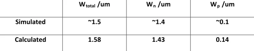
capacitance C’(depl) per unit area of the MOS capacitor in depletion mode is given as
[53]
1
1
1
'(
)
ox'
SDC depl
=
C
+
C
(2.1)Cox is the capacitance of the gate oxide (insulator) and, C’SD is the capacitance of the
depletion region. ox ox ox
C
t
ε
=
(2.2)'
s SD dC
t
ε
=
(2.3)where εox is the permittivity of the transparent insulator, εs is the permittivity of
silicon, tox is the thickness of the transparent insulator, td is the depletion region
width. Considering Equation (2.2) and (2.3), Equation (2.1) can be written as
'(
)
oxox ox d s
C depl
t
t
ε
ε
ε
=
+
(2.4)Assuming the phase shifter is working in depletion mode with the maximum
41 | P a g e
determined by the doping level of the silicon substrate. The depletion region reaches
its maximum width when the inversion layer which is a thin layer of minority carriers
occurs at the insulator-semiconductor interface. Once the doping level of the silicon
substrate is fixed, according to Equation (2.4), the capacitance C’(depl) is a function
of the permittivity of the transparent insulator material and its thickness. The total
capacitance of the MOS capacitor can then be written as
'(
)
ox
ox
ox d
s
C
S
C delp
S
t
t
ε
ε
ε
= ×
=
+
(2.5)where S is the area of the MOS capacitor.
The maximum depletion region width tdT can be written as [53]
1/2
4
(
s fn)
dT d
t
eN
ε φ
=
(2.6)with e=1.6×10⁻¹⁹ C the electronic charge. The potential φfn is the difference between
the intrinsic Fermi energy EFi and Fermi energy EF, which is given by
ln(
d)
fn t
i
N
V
n
φ
=
(2.7)where Vt=0.0259 V is the thermal voltage at 300 K, Nd is the donor doping
42 | P a g e
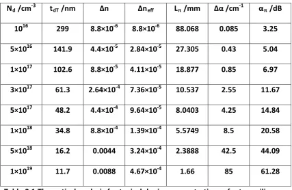
The silicon layer of silicon-on-insulator (SOI) wafer used in this work is 220
nm thick. The effective refractive index change is obtained by converting the change
of carrier concentration into a refractive index change via the plasma effect. At the
meantime, the overlap between the optical mode and the carrier density changing
region must be taken into account. As a simple approximation, by assuming carrier
concentration in the depletion region is zero and that outside the depletion region
equals the doping concentration, the effective refractive index change ∆neff is given
as dT eff si
t
n
n
t
∆
=
∆
(2.8)where tsi is the thickness of the silicon layer. In n-type silicon, the total free carrier
density change is mainly the electron density change, ∆N≈∆Ne. And also in full
depletion condition, the electron density change in MOS capacitor equals the n-type
doping concentration, ∆Ne≈Nd. Therefore, combining with Equation (1.7), Equation
(2.8) can be written as
22
8.8 10
dTeff d si
t
n
N
t
−∆
= −
×
(2.9)By calculating Equation (2.6) and (2.9) which are both functions of doping
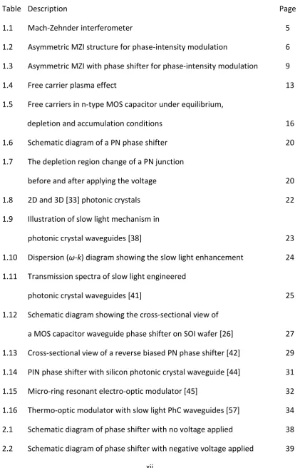
concentration, the maximum depletion region width and effective refractive index
43 | P a g e
shows that the depletion region width scales inversely with doping concentration.
The ∆neff curve shows the effective refractive index change due to electron density
change. Fig.2.3 shows that with increasing the doping density, the maximum
depletion region width decreases, while the effective refractive index change
increases.
Fig.2.3 Maximum depletion region width (tdT) and effective refractive index change
due to electron density change (∆neff) in MOS capacitor working in depletion mode
with different doping concentrations (Nd). The tdT curve is generated by calculating
Equation (2.6) and (2.7), assuming the insulator layer thickness is zero. The ∆neff
curve is produced by calculating Equation (2.9). In n-type silicon, the electron density is roughly the n-type doping density, ∆Ne≈Nd.
Ideally, it is better to have the entire silicon layer depleted by the applied
voltage. As a result, the optical mode in silicon waveguide experiences the same
refractive index change. Otherwise, the non-uniform refractive index changes the