Suitable thicknesses of base metal and interlayer and
evolution of phases for Ag/Sn/Ag transient liquid phase
joints used in power die attachment
J.F. Li
*, P.A. Agyakwa, C.M. Johnson
Department of Electrical and Electronic Engineering, The University of Nottingham, University Park, Nottingham NG7 2RD, United Kingdom
Abstract
Both real Si insulated gate bipolar transistors (IGBT) with conventional Ni\Ag
metallization and a dummy Si die with thickened Ni\Ag metallization have been bonded on
Ag foils electroplated with 2.7 m and 6.8 m thick Sn as an interlayer at 250ºC for 0 min, 40
min and 640 min. From microstructure characterization of the resulting joints, suitable
thicknesses are suggested for the Ag base metal and the Sn interlayer for Ag/Sn/Ag transient
liquid phase (TLP) joints used in power die attachment, and the diffusivities of Ag and Sn in
the Ag phase are extracted. In combination with the kinetic constants of Ag3Sn growth and
diffusivities of Ag and Sn in Ag reported in the literature, the extracted diffusivities of Ag and
Sn in Ag phase are also used to simulate and predict the diffusion-controlled growth and
evolution of phases in the Ag/Sn/Ag TLP joints during an extended bonding process and in
service.
Keywords: Transient liquid phase (TLP) bonding; Die attachment; Diffusion; Interfacial
reaction; Intermetallic compounds; Solid solution
1. Introduction
Transient liquid phase (TLP) bonding used in electronic packaging and interconnects is
one of the promising alternative joining technologies for high temperature and high power
density power electronics [1-4]. This is because such a TLP joint can formed through a lower
melting point Sn or In interlayer, reacting with and/or diffusing into a surrounding base metal
under extended isothermal solidification. The TLP bonding can hence be processed at
relatively low temperatures similar to those for conventional soldering process while resulting
in higher remelt temperatures of the produced joints [4]. Therefore, the TLP joints are
expected to be more creep resistant and more reliable than the conventional Sn-based solder
joints for applications at elevated temperatures.
As introduced in two previous papers [5,6], directed towards electronic packaging and
interconnects, TLP bonding used to join base metals Ag, Au and Cu has been extensively
investigated [3-13], while that to join base metals Ni, Pd, Pt and Zr has also been reported
[14-16]. Within acceptable bonding temperatures and times, the produced TLP joints
generally consist of intermetallic compounds (IMCs) of those base metals and Sn, In, InSn,
SnBi, BiIn2 or SnInBi interlayer. Despite the fact that the IMCs are more brittle than the
corresponding base metals, they have much higher mechanical strength and creep resistance
than the conventional Sn-based solders used in electronic packaging and interconnects.
Indeed, significantly improved reliability of the TLP joint consisting of Cu6Sn5 and Cu3Sn
IMCs and used to attach 1200 V and 150 A Si IGBTs on a type of ceramic-based substrates
had been demonstrated by means of active power cycling experiment under the maximum
juncture temperatures of 165 C to 171 C [17].
The present work is concerned with the Ag/Sn/Ag TLP system in which the formation
and evolution sequence of the intermetallic phases can be predicted using the binary Ag-Sn
phase diagram as shown in Fig. 1 [18]. The feasibility of using this system for joining
1980s [4,7]. In a previous paper [5], the thickening kinetics of Ag3Sn IMC growth was
investigated by sandwiching a thin layer of Sn between two pieces of Ag foil at temperatures
of 260 C, 300 C and 340 C. In the present paper, both real Si IGBTs with conventional
Ni\Ag metallization and dummy Si dice with thickened Ni\Ag metallization have been
bonded on the Ag foils electroplated with 2.7 m and 6.8 m thick Sn as interlayer at 250 ºC
for 0 min, 40 min and 640 min. Then the microstructure features in terms of phases, voids and
thicknesses of the resulting joints were characterized and analyzed. The objectives of this
paper are: (i) to determine suitable thicknesses of interlayer Sn and base metal Ag on both the
power die and the supporting substrate for the Ag/Sn/Ag TLP system which can be used in
power die attachment; (ii) to extract and report the diffusivities of Ag and Sn in Ag IMC
which are lack in the existing literature; and (iii) to simulate the diffusion-controlled growth
and evolution of phases in the Ag/Sn/Ag TLP joints during extended bonding process, which
can be used to predict the phases stably existing in the Ag/Sn/Ag TLP joints in service.
Given the fact that the conventional Sn-based solder joints are in general not reliable at
temperatures above 125C, the results obtained from the present work will be useful for
utilizing the Ag/Sn/Ag TLP joints in the development and manufacturing of high temperature
power electronic systems. For instance, it is desirable to develop power electronics modules
which are reliable in continuous operation in an ambient temperature of 150 °C and above for
periods of several years. Examples includes aerospace where there is an increasing move to
electronic rather than hydraulic or pneumatic systems, automotive under-hood applications in
conventional, hybrid and electric drive systems and down-hole gas and oil field applications.
The Ag/Sn/Ag TLP joints are well suited to these applications and even able to operate at
temperatures higher than the processing temperature.
2.1 Preparation of samples
The real Si IGBTs used in this work are 13130.3 mm in size and have the
conventional 0.8\0.7 m thick Ni\Ag metallization, and the dummy Si dice are 13131 mm
Si chips with thickened 1\6 m thick Ni\Ag metallization deposited using sputtering process.
They were both obtained from Dynex Semiconductor Ltd (Doddington Road, Lincoln LN6
3LF, UK), and their cross-sectional scanning electronic microscopy (SEM) images are shown
in Fig. 2. The as-received Ag foils electroplated with 2.7 m and 3.1 m, or 6.8 m and 7.5
m thick Sn on both sides were discs of 100 mm in diameter and 100 m in thickness of Ag.
They were obtained from Applied Materials Technology Ltd (Units 6 &7 Lyndon Business
Park, Farrier Road, Lincoln LN6 3RU, UK), and their cross-sectional SEM images are given
in Fig. 3.
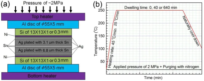
All the samples were prepared using a sample configuration and temperature/pressure
profile schematically illustrated in Fig. 4. The as-received Ag discs plated with the Sn layers
were first cut into pieces of 1313 mm in size. Then a real Si IGBT (or a dummy Si chip) was
placed in contact with the surface of a 1313 mm Ag foil plated with 2.7 m thick Sn, and
another real IGBT (or another dummy Si chip) was placed in contact with the surface of
another 1313 mm Ag foil plated with 6.8 m thick Sn. Next, they were brought together, and
put in a house-made bonding rig, where they were inserted into two 555 mm Al discs to
improve the uniformity of heat delivered from both the top and bottom electrical cartridge
heaters during the final bonding process. Following this, a pressure of ~2MPa was applied to
the bonding area, and the samples were purged with nitrogen gas (760 mL/min at 1.5 bar).
The bonding process was started by subjecting the samples to a temperature profile which
involved first heating up to 200 C at a heating rate of 45 C/min, then heating up to 250 C at
a heating rate of 25 C/min that the bonding rig could comfortably achieve, before holding at
were taken out of the bonding rig once it cooled down to 100 C with a time approximately of
10 min.
The combinations of Si die, Ag foil and dwelling time considered during the above
bonding process and their sample codes are listed in Table I. The focus of the present work is
the interfacial reactions and microstructures in the Ni/Ag/Sn/Ag and Ag/Sn/Ag/Ni parts of the
bonding structure shown in Fig. 4a. The result obtained will be used to determine suitable
thicknesses of interlayer Sn and base metal Ag on both the power die and the supporting
substrate for the Ag/Sn/Ag TLP system which can be used in power die attachment. It should
be pointed out that a certain amount of Sn was found to squeeze out of the bonding areas in
all the samples of the real Si IGBTs and dummy Si chips bonded on the Ag foil plated with
6.8 m thick Sn. However, no appreciable amount of Sn could be observed outside the
bonding areas in all the samples of the real Si IGBTs and dummy Si chips bonded on the Ag
foil plated with 2.7 m thick Sn.
Metallographic cross-sections of all the bonded samples listed in Table I were prepared
for the microstructural characterization and thickness measurement of the IMCs formed in the
bonded samples. The samples were first mounted in epoxy resin that was cured at room
temperature for 24 hours. The mounted samples were then successively ground with 800,
1000 and 1200 grit SiC papers and finally polished using diamond slurries of 3 μm and 1 μm
both for 10 min.
2.2 Characterization and thickness measurement of IMCs
A JEOL 6400 SEM (JEOL Ltd, 1-2, Musashino 3-chome Akishima Tokyo 196-8558,
Japan) using a backscattered electron signal was employed for the imaging and analysis of
microstructural features. The IMCs formed in the bonded samples were identified using an
Oxford Instruments ISIS energy-dispersive X-ray spectroscopy (EDXS) microanalysis system
the SEM. As presented in the results, from the SEM images, it is hard to determine the
interface between the Ag3Sn and Ag IMCs even if both of them had been formed in some of
the bonded samples. Therefore, the total thicknesses of the Ag3Sn and Ag IMCs formed in
all the bonded samples and the thicknesses of the Ni3Sn4 IMC formed in the samples of
attaching the real IGBTs were measured using an image analysis method as detailed
elsewhere [5,6]. The image analysis was performed utilizing the Image Processing Toolbox
Version 5.0.0 of MATLAB R14SP2 (The Mathworks, Matrix House, Cambridge Business
Park, Cambridge CB4 0HH, UK). For each sample, three images 512×416 pixels in
resolution, one 200×160 μm and two 40×32 μm in size, were used. A data series for the
thickness of each layer in a sample was obtained from 512×3=1536 intercepted lengths in the
through-thickness direction. The resulting thicknesses were given in terms of mean, standard
deviation (Std. Dev.), minimum and maximum values.
In order to obtain the individual thicknesses of Ag3Sn and Ag IMCs formed in some of
the bonded sample for extracting the diffusivities of Ag and Sn in Ag IMC, focused ion
beam (FIB) ion channelling was employed to observe the grain morphology, size and
boundaries of the IMCs formed in samples C1 and C2. This was done using the FEI
Quanta200 3D DualBeam FIB/SEM (FEI, Europe NanoPort, Achtseweg Noord 5, 5651 GG Eindhoven, The Netherlands) to progressively mill the polished cross sections, which
provided grains and grain boundary contrast.
3. Results
3.1 Real Si IGBTs with conventional Ni\Ag metallization
There was no noticeable difference in the microstructure features of the real Si IGBTs
bonded on the Ag foil plated with 2.7 m thick Sn from those of the real IGBTs bonded on
samples of real IGBTs bonded on the Ag foil plated with 2.7 m thick Sn. Ag-Sn IMCs could
be observed at the Ag foil side only, and the Ni barrier layer underneath the top Ag
metallization of the real IGBTs had fully been reacted with Sn into Ni3Sn4 for all the three
samples. This is quite unusual and will be further discussed in the section of discussion
below.
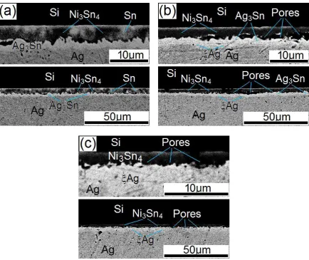
For sample A0 bonded at 250 C for 0 min, there was only Ag3Sn IMC which could be
detected by EDXS at the Ag foil side. There was trace Sn remaining and mixed with the
Ni3Sn4 IMC formed at the IGBT side. For sample A1 bonded at 250 C for 40 min, there were
both Ag3Sn and Ag IMCs which could be identified by EDXS at the Ag foil side. It could be
detected with EDXS that the Ag3Sn IMC dominated the thickness of the Ag-Sn IMCs, but the
interface between Ag3Sn and Ag IMCs was hard to be viewed from the SEM image. At the
IGBT side, there was no appreciable pure Sn remaining any more, but there was a chain of
voids of several microns in size along the interface of the Ni3Sn4 IMC in contact with the
Ag3Sn IMC at the Ag foil side. For sample A2 bonded at 250 C for 640 min, there was only
Ag IMC left at the Ag foil side. The Ni3Sn4 IMC and a chain of voids of several microns in
size formed at the IGBT side were both similar to those observed in the sample A1 bonded at
250 C for 40 min.
The total thicknesses measured with the image analysis method for the Ag-Sn IMCs
formed in all the bonded samples are listed in Table II. The means, standard deviations and
maximum values for the samples A0 to A2 are almost the same as those for samples B0 to
B2, respectively. The mean thicknesses for the samples A0, A1, B0 and B1 are similar to each
other. This may be attributed to the Sn partially squeezed out of the bonding areas in the
samples B0 and B1 that were bonded on the Ag foil plated with thicker Sn. On the other hand,
the mean thicknesses for the samples A2 and B2 are clearly larger than those for the samples
early bonding stage had been converted into Ag IMC, which thus increased the total
thickness of the Ag-Sn IMCs during the late bonding stage. In addition, the ratios of the
maximum to the mean thicknesses of the Ag-Sn IMCs in the samples A0 and B0 are equal or
close to 2, while those in the samples A1, A2, B1 and B2 are somewhat lower than 2.
Also measured with the image analysis method, the mean thicknesses of the Ni3Sn4
IMC formed at the IGBT sides were both approximately 4.0 µm for samples A0 and B0, and
all in the range of 2.0 to 2.5 µm for samples A1, A2, B1 and B2.
3.2 Dummy Si Chips with thickened Ni\Ag metallization
As shown in Figs. 6 and 7, if the dummy Si chips with 1\6 m thick Ni\Ag metallization
were bonded on the Ag foil plated with 2.7 m thick Sn, the Ni barrier layer underneath the
Ag layer was intact and some residual Ag was retained at the chip side in both samples C1
and C2. For sample C1 bonded at 250 C for 40 min, the joint mainly consisted of relatively
coarse Ag3Sn grains plus finer Ag grains which were similar to each other at both the chip
side and the Ag foil side (Fig. 7a). For sample C2 bonded at 250 C for 640 min, the joint
consisted of Ag grains only which were also similar to each other at both the chip side and
the Ag foil side (Fig. 7b).
As can be seen from Fig. 8, if the dummy Si chips with 1\6 m thick Ni\Ag
metallization were bonded on the Ag foil plated with 6.8 m thick Sn, the Ni barrier layer
underneath the Ag layer was locally attacked by Sn to produce Ni3Sn4 IMC at the chip side.
This reveals that the liquid Sn layers in the bonding areas of these samples were somewhat
thicker than those in the bonding areas of the samples C1 and C2 during the initial bonding
stage. After the Ag layers on the Si chips were consumed, certain amounts of residual Sn were
delivered to react with the Ni barrier layers, through the grain boundaries and/or molten
channels existing between the Ag3Sn crystals formed during the early stage. For sample D1
chip side, and major Ag3Sn IMC plus minor Ag IMC at the Ag foil side. For sample D2
bonded at 250 C for 640 min, the joint also consisted of Ag3Sn IMC plus local Ni3Sn4 IMC
at the chip side. However, at the Ag foil side, the joint consisted of major Ag IMC plus
minor Ag3Sn IMC. Note that the Ag-Sn IMCs could be observed at both the Si chip side and
the Ag foil side in the samples D1 and D2, which are somewhat different from those in the
samples A1 and A2 where the Ag-Sn IMCs was observed at the Ag foil side only (Fig. 5).
As listed in Table II, the total thickness of the Ag-Sn IMCs formed in sample C2 is
larger than that of the Ag-Sn IMCs formed in sample C1. This can be related to the change of
the Ag3Sn IMC formed during the early bonding stage into Ag IMC during the late bonding
stage. However, the total thickness of the Ag-Sn IMCs formed in sample D2 is similar to that
of the Ag-Sn IMCs formed in sample D1. This may be due to the fact that different amounts
of liquid Sn had partially been squeezed out of the bonding areas in samples D1 and D2
during the early bonding stage.
Comparing the total thicknesses of the Ag-Sn IMCs formed in the samples C1, C2, D1
and D2 with those formed in the samples A1, A2, B1 and B2, it can further be seen that the
former values are all larger than two times of the latter values. This indicates that less
amounts of Sn were available to react with Ag in the samples A1, A2, B1 and B2 than in
samples C1, C2, D1 and D2. Therefore, the reaction rate of the liquid Sn with the Ni barrier
layer was probably higher than that of the liquid Sn with the Ag in the samples of the real
IGTBs bonded on the Ag foils.
In addition, the separate thicknesses of Ag3Sn and Ag IMCs formed in the sample C1
will be used to extract the diffusivities of Ag and Sn in Ag as presented below. They can be
separated from the total thickness listed in Table II, with the help of the FIB image shown in
Fig. 7a. The values of 5.9 m and 2.0 m were estimated for the thicknesses of the Ag3Sn
respectively.
4. Discussion
4.1 Interfacial microstructure
As can be seen from Fig. 1, the solubility of Ag in liquid Sn at 250 ºC is around 5 at%,
and the amount of Ag dissolved into the liquid Sn during the bonding process should be
negligible. Therefore, the result of Ag-Sn IMCs observed only at the Ag foil side in all the
samples of attaching real IGBTs cannot be attributed to the dissolution of 0.7 µm Ag into the
2.7 µm (and even 6.8 µm thick) liquid Sn during the early bonding stage. More likely, this
may be related to the rapid coarsening of relatively small Ag3Sn scallops and can be
explained as follows.
The effect of the initial dissolution of Ag and nucleation of Ag3Sn may be ignored
because they were extremely rapid. Following our previous work on the Ag/Sn/Ag TLP
system [5], until the liquid Sn was consumed, only Ag3Sn scallops were formed between the
Sn and Ag. The evolution of the average thickness of the Ag3Sn layer with respect to bonding
time can be described using the following Eq. (1) [5]:
max , 3 / 1 3 3 3
3 ) , 0
87 . 18 17 . 37 exp( 10 573 ..
3 Ag Sn Ag Sn
Sn
Ag t x x
RT
x (1)
Where xAg3Sn is the average thickness of the Ag3Sn layer in m, t is time in s, R is the
universal gas constant, T is the absolution temperature, and xAg3Sn,max is maximum thickness of
the Ag3Sn layer which the Sn interlay is consumed to produce according to the reaction Eq.
(2):
Sn Ag Ag
Sn3 3 (2)
If Eqs. (1) and (2) are extended to relatively low bonding temperature until the melting
point of eutectic Sn-3.5Ag alloy, 221 ºC, they may be used to calculate the growth of the
early bonding stage. The calculated results for the bonding temperatures of 221 ºC and 250 ºC
are shown in Fig. 9, where the densities of Sn, Ag and Ag3Sn used during the calculation are
listed in Table III. It can be seen that a layer of 0.7 µm thick Ag reacting with ~0.35 µm thick
Sn (~0.7 µm thick Sn in total for two sides) produces ~1 µm thick Ag3Sn IMC at one side of
the Ag/Sn/Ag TLP sample. This takes only 2 min and 0.4 min at the bonding temperatures of
221 ºC and 250 ºC, respectively. Therefore, based on the temperature profile shown in Fig.
4b, the bonding times for the Sn interlayer to stay above the melting point should have been
sufficient to consume the 0.7 µm thick Ag metallization on the all real IGBTs of the present
TLP samples, even for a bonding time of 0 min at 250 ºC.
As also reported in the previous work [5], the growth of the Ag3Sn IMC between liquid
Sn and solid Ag could be well explained by the grain boundary-/molten channel-controlled
growth. Once the 0.7 µm thick Ag on one IGBT was consumed, liquid Sn remaining would
thus penetrate through grain boundaries between the Ag3Sn IMC crystals to further rapidly
attack and react with the Ni layer under the original Ag metallization, forming the Ni3Sn4
IMC at the IGBT side. With decreasing the amount of the liquid Sn, the Ag3Sn IMC crystals
or scallops formed at the two sides gradually came into contact with each other. Relatively
small Ag3Sn IMC crystals or scallops formed at the two sides tended to coalesce into
relatively large Ag3Sn scallops as they formed and grew. This was probably the reason why
the Ag-Sn IMCs were observed only at the Ag foil side in all the samples of attaching real
IGBTs (Fig. 4). In the samples of attaching the dummy Si chips with thickened Ag
metallization, the Ag3Sn scallops formed at the two sides had already been too large to further
coarsen before they come into contact with each other. Therefore, in these samples, the Ag3Sn
scallops were observed at both the chip side and the Ag foil side (Figs. 5 and 7).
Given the fact that the average thicknesses of the Ag-Sn IMCs in samples A0, A1, B0
average thickness of the Ag consumed on the Ag foil side in these samples was also ~0.7 µm.
The rate of the reaction between the liquid Sn and the Ag foil might be the same as or lower
than that between the liquid Sn and the Ag metallization on the IGBT. Nevertheless, only
~0.7 µm thick Sn interlayer was consumed by ~0.7 µm (~1.4 µm in total for the two sides)
thick Ag on both the IGBT and Ag foil sides to form the Ag3Sn IMC (Fig. 9). More amount
of the Sn interlayer, i.e. ~2.0 µm thick Sn if the Sn interlayer was 2.7 µm in thickness, was
consumed by the Ni layer to produce the Ni3Sn4 IMC on the IGBT side in each of these
samples. According to the following reaction Eq. (3):
4 3
3
4Sn NiNi Sn (3)
With the densities of 7.36, 8.91 and 8.65 g/cm3 for Sn, Ni and Ni3Sn4, the consumption of 2.0
µm thick Sn would require 0.6 µm thick Ni and produce 2.3 µm thick Ni3Sn4 IMC. They are
in good agreement with the thickness of 0.8 µm for the Ni layer on the IGBTs and the
thicknesses in the range of 2.0 to 2.5 µm for the Ni3Sn4 IMC formed in samples A1, A2, B1
and B2. The relatively thicker ~4.0 µm thick Ni3Sn4 IMC formed in samples A0 and B0 may
be attributed to the existence of boundaries between the Ni3Sn4 IMC grains. With increasing
the bonding time, the Ni3Sn4 IMC grains ripened and the grain boundaries migrated and
developed into a chain of voids along the interface between the Ni3Sn4 IMC and the Ag-Sn
IMCs as shown in Fig. 5. In addition, as aforementioned, the microstructural characterization
and mean thicknesses of both the Ag-Sn IMCs and the Ni3Sn4 IMC in samples A0 to A2 were
similar to those in the corresponding samples B0 to B2. This reveals that around 4 µm thick
liquid Sn had probably been squeezed out of the bonding areas during the preparation of
samples B0 to B2.
The solubility of Ni in liquid Sn is even lower than that of Ag at a same temperature
[19]. The Ni3Sn4 IMC on the IGBT side should hence have been formed through the
produce Ni3Sn4 IMC was also reported to be grain boundary-/molten channel-controlled
[20,21]. The trace Sn mixed with the Ni3Sn4 IMC was observed in the sample formed at 250
ºC for 0 min because it was trapped within the grain boundaries and/or molten channels. The
start of the reaction of the solid Ni with the liquid Sn was later than that between the solid Ag
on both the IGBT and the Ag foil sides with the liquid Sn. However, the reaction of the Ni
with Sn still consumed much more amount of the liquid Sn than the reaction of the Ag with
Sn. This reveals that the interfacial reaction between the liquid Sn and the Ni layer was
extremely rapid when compared with that between the liquid Sn and both the Ag metallization
and the Ag foil. Such a result is not in agreement with the kinetic constants for the growths of
Ni3Sn4 and Ag3Sn scallops reported in the existing literature [5,20,21]. This may be
associated with the application of pressure in the present bonding process, but further
investigation is needed to provide true understanding.
4.2 Suitable thicknesses of Ag and Sn layers for die attachment
To achieve improved reliability, the processed Ag/Sn/Ag TLP joints used in power die
attachment should contain neither any Sn remaining nor any Ni3Sn4 IMC in contact with the
Ag3Sn IMC. This is because the Sn remaining with low melting point has relatively poor
mechanical strength and creep resistance. In particular, when the operating temperature is
close to and/or above the melting point, the mechanical strength of the joint will be reduced
significantly or even lost. On the other hand, the ripening process of the Ni3Sn4 grains would
lead to the formation and growth of a chain of voids between the Ag3Sn and Ni3Sn4 IMCs as
shown in Fig. 5, during the extended bonding stage and/or in the high temperature
applications. They would not only deteriorate the thermal performance of the joints, but also
act as the sites for nucleation and growth of cracks. Therefore, the existence of both the Sn
remaining and the Ni3Sn4 IMC in contact with the Ag3Sn IMC in the Ag/Sn/Ag TLP joints
As mentioned previously, before the liquid Sn remaining was consumed, the thicknesses
of the Ag3Sn IMC formed and the Ag layers required to consume different thick Sn
interlayers can be simply calculated with Eqs. (1) and (2). However, because of the grain
boundary-/molten channel-controlled growth of the Ag3Sn IMC between liquid Sn and solid
Ag and the non-flat interfaces between the formed Ag3Sn IMC and the residual Ag, local Ag
might be consumed more and quicker than the rest of the Ag layer to react with the liquid Sn
to produce Ag3Sn IMC during the bonding process. As a result, the Ag layers to be deposited
on the power die side and the substrate side as base metal layers should be thicker than those
calculated according to the above reaction Eq. (2). Otherwise, once local Ag layer is
consumed, Sn atoms will be rapidly delivered through the grain boundaries /molten channels
existing between the Ag3Sn crystals to attack the Ni layer and produce Ni3Sn4 IMC. This can
be further verified by the formation of local Ni3Sn4 IMC in the present samples D1 and D2 as
shown in Fig. 8. Despite the fact that the original thickness of the Sn interlayer in both
samples was 6.8 m, the actual thickness of the Sn interlayer in the bonding areas should be
thinner than 6 m which can approximately consume 6 m thick Ag on both the dummy Si
chip side and the Ag foil side (Fig. 9). This is because the Sn was observed to be partially
squeezed out of the bonding areas in both samples during the bonding process, as
aforementioned.
Again as reported in the previous paper [5], before the Ag3Sn grains formed at the two
sides of the Ag/Sn/Ag samples came into contact with each other, the ratios of the maximum
to the mean values for the Ag3Sn IMC thicknesses in the different samples were in the range
of 1.9 to 2.6. Similar ratios of the maximum to the mean values for the Ag3Sn IMC
thicknesses were also observed in the present samples A0 and B0. They are in good
agreement with the steady-state particle coarsening theories, which predict an upper limit on
factor of at least 2 to increase the thickness of the Ag layer that is needed to consume the Sn
interlayer for producing Ag3Sn IMC. This may avoid the Ni barrier layer underneath the Ag
layer to be attacked by the liquid Sn during the TLP bonding process. In such a case, the
thickness of the Ag layers needs to be deposited on both the power die and the supporting
substrate should be at least two times the entire thickness of the Sn interlayer in the middle.
For example, if the total thickness of the Sn interlayer is 2 m, there should be at least 4 m
thick Ag layers deposited on both the power die and the supporting substrate.
Given the difficulty in depositing Ag layers thicker than 10 m on semiconductor
power devices, the Sn interlayers used for producing the Ag/Sn/Ag TL joints should generally
be thinner than 5 m. A more suitable thickness of the Sn interlayer may be 2 to 3 m, in
combination with a thickness of 4 to 6 m for the Ag layers that are easy to be deposited on
both the semiconductor power die and the supporting substrate. As demonstrated by the
present result shown in Figs. 6, and 7, such a combination of the thicknesses for the Sn
interlayer and the Ag base metal layers can indeed be used to produce good quality of
Ag/Sn/Ag TLP joints.
4.3 Diffusivities of Ag and Sn in Ag IMC
Before the Sn remaining was consumed, no Ag IMC was detected in all the Ag/Sg/Ag
samples reported in the previous paper [5]. We may hence assume that the Ag IMC started to
form and grow at the time when the Ag3Sn IMC layer in the samples had already reached to
its maximum thickness according to the reaction Eq. (2). Also, we may ignore the timescale
for the nucleation of the Ag crystals and assume that the thickening of the Ag layer is
diffusion-controlled at the expense of the Ag3Sn layer formed previously. Furthermore, we
may assume that the diffusion of Ag and Sn in both the Ag IMC and Ag phases are governed
by the Darken interdiffusion coefficient [23]:
Ag Sn Sn
Sn
Sn N D N D
N
Where D(NSn) is Darken interdiffusion coefficient, NSn is Molar fraction of Sn, DSn and DAg
are the diffusivities of Sn and Ag both in the Ag IMC or both in the Ag phases. Under these
assumptions, the thicknesses of the Ag3Sn and Ag IMCs in the present samples C1 and C2
can be used to extract the diffusivities of Ag and Sn in the Ag IMC as described below.
First, with the kinetic constants of Ag3Sn growth reported in the previous paper [5], if
the effect of the initial dissolution of Ag and nucleation of Ag3Sn was ignored, the evolution
of the average thickness of the Ag3Sn layer with respect to bonding time can be described
using Eq. (1). Eq. (1) in combination with the reaction Eq. (2) can be used to calculate the
time, t0, when the Sn interlayer was consumed, as well as the growth of the Ag3Sn IMC and
the consumptions of the Ag base metal layers and the Sn interlayer during the early bonding
stage.
Then the growth of the Ag IMC at the expense of the Ag3Sn IMC formed previously
and subsequent evolution of the Ag IMC with respect to bonding time can be simulated with
a fixed-grid numerical method detailed elsewhere [24,25]. Essentially, this numerical method
can be used to obtain the distribution and evolution of the Molar fractions, NSn, across the
Ag/Sn/Ag TLP joints as schematically illustrated in Fig. 10 with respect to bonding time,
based on Fick’s diffusion law. The governing equations are given by:
5 ,..., 1 ), ( ) ( , )] , ( / ) , ( [ ) ( )] , ( / ) , ( [
1
t x S t i
S x t x V t x N N D x t t x V t x N i i Sn Sn Sn (5) 4 ,..., 1 , ), ( , ) ( ] / / [ )] , ( / ) , ( [ ) ( )] , ( / ) , ( [ ) ( ) ( ) ( i t S x t t S V N V N x t x V t x N N D x t x V t x N N D i i i i i i t S x Sn Sn i t S x Sn Sn i i i (6)
They are subject to the following boundary conditions:
0 0( )
1 5( )
0 )] , ( / ) , ( [ L t S x x t x V t x NSn (7b)
And the initial conditions can be given as:
) ( ) ( ), , ( / ) , ( ) , ( / ) ,
(x t V x t N x t0 V x t0 S0 t0 x S5 t0
NSn Sn (8)
Where x is position coordinate, V is Molar volume, L0 and L1 are two boundaries of one TLP
joint, Si (i=1,…,4) are moving interfaces of phases, and superscripts – and + stand for left and
right sides of the moving interfaces.
In the present work, the values used in the simulation for the Molar fraction of Sn,
density and Molar volume of the different phases and the interfaces in the Ag/Sn/Ag TLP
joints are listed in Table III. They were calculated based on the binary Ag-Sn phase diagram
and the lattice cell parameters reported in Refs. [18,26-32]. Inside each of the phases, the
density and Molar volume were assumed to be linearly related to the Molar fraction of Sn.
The diffusivities of Ag and Sn in Ag estimated from the Arrhenius-type plots assessed in Ref.
[21] were taken as known values to calculate the Darken interdiffusion coefficient of the Ag
phase. The stoichiometric width of the Ag3Sn IMC is extremely narrow and was taken as
zero, and hence the diffusion of atoms inside the Ag3Sn layer may be ignored. Under such an
assumption, the interdiffusion coefficients of the Ag3Sn layer can be taken as any value.
Data fittings of the measured thicknesses of Ag3Sn and Ag layers in the samples C1
and C2 to those simulated using the numerical method to solve the above Eqs. (5) to (8) has
been used to determine the diffusivities of Ag and Sn in Ag. For each simulation, at time t0,
there are Ag3Sn and Ag phases only in the Ag/Sn/Ag TLP joint, and their Molar fractions
were set as 0.25 and 0, respectively. During the simulation, the D(NSn) and V dependent on the
NSn were updated with an iteration method, and the calculation convergence was verified by
a relative error less than 1.010-4.
samples C1 and C2 to those simulated using the numerical method is plotted in Fig. 11. It can
be seen that the simulated Ag3Sn/Ag and Ag/Ag interfaces are in good agreement with the
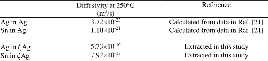
experimental solid points. The diffusivities of Ag and Sn in Ag IMC at 250 C determined
from the data fittings are 5.7310-16 m2/s and 7.9210-17 m2/s as listed in Table IV. They are
approximately seven and three orders of magnitude higher than those of Ag and Sn in Ag at
the same temperature of 250 C, respectively. On the other hand, they are slightly higher than
the volume diffusivities of Ag and Sn in Ag3Sn IMC, but significantly lower (four to six
orders of magnitude lower) than the grain-boundary diffusivities of Ag and Sn in Ag3Sn IMC
reported in Ref. [33].
4.4 Evolution of phases during extended bonding process
With the extracted diffusivities of Ag and Sn in Ag IMC at 250 C, the evolution of
phases in two Ag/Sn/Ag TLP joints during the extend bonding process have been simulated
with the same numerical method to solve Eqs. (1) and (5) to (8). One of the joints was
assumed to produce using 2 m thick Sn interlayer sandwiched between two layers of 7 m
thick Ag base metal. The other one was assumed to produce using 4 m thick Sn interlayer
sandwiched between two layers of 14 m thick Ag base metal. The combined thicknesses of
Sn interlayer and Ag base metal layers in both simulated joints were selected for achieving
the final joints consisting of the solid solution of Sn in Ag with a Sn Molar fraction of 0.0835,
which is slightly lower than the equilibrium Sn Molar fraction of 0.085 at the interface of Ag
in contact with Ag IMC [18].
The simulated results are shown in Fig. 12 where the horizontal axes are in logarithmic
scale. It can be seen that the timescales for consuming the Sn interlayers to produce Ag3Sn
IMC are two orders of magnitude shorter than those for consuming the Ag3Sn IMC layers
formed previously to produce Ag IMC. Given that the fact that the initial dissolution of Ag
them during the early bonding stage on the extracted diffusivities of Ag and Sn in Ag IMC
should be negligible.
It can be noted that the Ag IMC will continue to grow after the Ag3Sn IMC is
consumed. This can be attributed to the net diffusion of Sn atoms towards the Ag\Ag
interfaces, from the part of the Ag IMC in the middle of the joints formed during earlier
stage and with higher Molar fractions of Sn. The bonding times for consuming the Ag3Sn
IMC to produce the Ag IMC and for consuming the Ag IMC to form the final solid solution
of Sn in Ag are 280 min and 6.5109 min in Fig. 12a, and 1120 min and 2.601010 min in
Fig.12b. With these timescales in mind, it is more realistic to process the Ag/Sn/Ag TLP
joints consisting of major Ag3Sn IMC plus minor Ag IMC and residual Ag for power die
attachment. Under the application environments, the temperatures can be lower than the 250
C used in the simulation, and the evolution rates of phases in this case would be much slower
than those shown in Fig. 12. Therefore, the Ag/Sn/Ag TLP joints can be expected to consist
of Ag IMC plus residual Ag during the majority of service lifetime if the Ag/Sn/Ag TLP
joints are applied in power die attachment.
If the thicknesses of the Ag base metal on both the power die and the supporting
substrate sides are just 2 to 2.5 times of the thickness of the entire Sn interlayer, the processed
Ag/Sn/Ag TLP joints can still be expected to consist of major Ag IMC plus minor residual
Ag during the majority of service lifetime. This is because, on the one hand, under the
application temperatures, the evolution rates of phases in the TLP joints should be much
slower than those shown in Fig. 12. On the other hand, even if the Ag base metal layers are
consumed, any possible further solid/solid interfacial reaction between Ag IMC and Ni
barrier layer should also be very slow. This is because there is no ternary Sn-Ag-Ni IMC
existing in the Sn-Ag-Ni system [19], and the supply of Sn from the Ag IMC to Ni barrier
5. Conclusions
From the above results and discussion for the Ag/Sn/Ag TLP joints used in power die
attachment, the following conclusions can be drawn:
1) The thickness of the Ag base metal layers on both the power die and the supporting
substrate should be at least two times of the average thickness that is required to
consume the Sn interlayer for producing Ag3Sn IMC. Otherwise, the Ni barrier layer
underneath the original Ag layer will be locally attacked by liquid Sn to react into
Ni3Sn4 IMC, which may lead to the formation and growth to a chain of voids along
the interface between the Ni3Sn4 and Ag-Sn IMCs during extended bonding process
and/or in service.
2) A thickness of 2 m to 3 m for the Sn interlayer in combination with a thickness of
4 m to 6 m for the Ag base metal layers deposited on both the semiconductor
power die and the supporting substrate will be a suitable selection for producing the
Ag/Sn/Ag TLP joints used in power die attachment. Such a combination of Sn
interlayer and Ag base metal layers for producing good quality of Ag/Sn/Ag TLP
joints has been demonstrated by the results shown in Figs. 6 and 7.
3) The diffusivities of Ag and Sn in Ag IMC at 250 C determined from the data
fittings of the measured thicknesses of Ag3Sn IMC and Ag IMC layers to the
simulated results with a numerical method are 5.7310-16 m2/s and 7.9210-17 m2/s.
They are slightly higher than the volume diffusivities of Ag and Sn in Ag3Sn IMC,
but four to six orders of magnitude lower than the grain-boundary diffusivities of Ag
and Sn in Ag3Sn IMC reported in the existing literature.
4) Simulated results for the evolution of phases in the Ag/Sn/Ag TLP joints indicate
Ag3Sn IMC plus minor Ag IMC and residual Ag for power die attachment. The
Ag/Sn/Ag TLP joints can be expected to consist of major Ag IMC plus residual Ag
during the majority of service lifetime if the Ag/Sn/Ag TLP joints are applied in
power die attachment.
Acknowledgements
This research was supported by the UK Engineering and Physical Science Research
Council as part of the Innovative Electronic Manufacturing Research Centre (IeMRC) [grant
number EP/H03014X/1] and the European Commission through the Seventh Research
Framework Programme, CleanSky “Systems for Green Operations”.
Reference
[1] L. Bernstein, J. Electrochem. Soc. 113(12), 1282 (1966).
[2] C.C. Lee, C.Y. Wang, Thin Solid Films 208, 202 (1992).
[3] G.S. Matijasevic, C.C. Lee, C.Y. Wang, Thin Solid Films 223, 276 (1993).
[4] G. Humpston, D.M. Jacobson, Principles of Soldering (Materials Park, Ohio 44073-0002,
ASM International, 2004), pp. 230-235.
[5] J.F.Li, P.A. Agyakwa, C.M Johnson, Acta Mater. 58(9), 3429 (2010).
[6] J.F.Li, P.A. Agyakwa, C.M Johnson, Acta Mater. 59(3), 1198 (2011).
[7] D. E. Crees, G. Humpston, D.M. Jacobson, D. Newcombe, GEC J. Res. 6(2), 71 (1988).
[8] T.B. Wang, Z.Z. Shen, R.Q. Ye, X.M. Xie, F. Stubhan, J. Freytag, J. Electron. Mater.
29(4), 443 (2000).
[9] F. Bartels, J.W. Morris, G. Dalke, W. Gust, J. Electron. Mater. 23(8), 787 (1994).
[10] E. Lugscheider, K. Bobzin, M.K. Lake, Surf. Coat. Technol. 142-144, 813 (2001).
[12] E. Lugscheider, K. Bobzin, M. Maes, S. Ferrara, A. Erdle, Surf. Coat. Technol. 200(1-4),
444 (2005).
[13] S. Sommadossi, W. Gust, E.J. Mittemeijer, Mater. Chem. Phys. 77(3), 924 (2002).
[14] P.K. Khanna, G. Dalke, W. Gust, Z. Metallkd. 90(9), 722 (1999).
[15] N. Quitoriano, W.S. Wong, L. Tsakalakos, Y. Cho, T. Sands, J. Electron. Mater. 30(11),
1471 (2001).
[16] T. Studnitzky, R. Schmid-Fetzer, J. Electron. Mater. 32(2),70 (2003).
[17] K. Guth, N. Oeschler, L. Bower, R. Speckels, G. Strotman, N. Heuck, S. Krasel, A.
Ciliox, in Proceedings of 7th International Conference on Integrated Power Electronics
Systems, March 6-8, 2012, Nuremberg, Germany, pp. 380-384.
[18] "Binary Ag-Sn phase diagram," Facility for the Analysis of Chemical Thermodynamics
(FACT), Available from:
http://www.crct.polymtl.ca/FACT/phase_diagram.php?file=Ag-Sn.jpg&dir=SGTE.
[19] H.F. Hsu, S.W. Chen, Acta Mater. 52, 2541 (2004).
[20] G. Ghosh, J. Appl. Phys. 88, 6887 (2000).
[22] V. Tikare, J.D. Cawley, Acta Mater. 46, 1333 (1998).
[23] Z. Mei, A.J. Sunwoo, J.W. Morris Jr., Metall. Trans. A23, 857 (1992).
[21] G. Ghosh, Acta Mater. 49, 2609 (2001).
[24] J.F.Li, P.A. Agyakwa, C.M Johnson, J. Mater. Sci. 45, 2340 (2010).
[25] J.F.Li, P.A. Agyakwa, C.M Johnson, Intermetallics 40, 50 (2013).
[26] H.W. King, T.B. Massalski, Phil. Mag. 6, 669 (1961).
[27] W. Klement Jr., Transactions of the Metallurgical Society of Aime 233, 1182 (1965).
[28] R.H. Kane, B.C. Giessen, N.J. Grant, Acta Metall. 14, 605 (1966).
[29] C.W. Fairhurst, J.B. Cohen, Acta Crystallogr. B28, 371 (1972).
[31] Y. Ning; X. Zhou, J. Alloys Compd. 182, 131 (1992).
[32] E. Roennebro, J. Yin, A. Kitano, M. Wada, T. Sakai, Solid Stat. Ion. 176, 2749 (2005).
Fig. 1. Phase diagram of binary Ag-Sn system.
Fig. 2. SEM images taken from the polished cross sections of: (a) real IGBT with
[image:24.595.80.517.340.517.2]
Fig. 3. SEM images taken from the polished cross sections of 100 m thick Ag foil
electroplated with: (a) 2.7 m thick Sn; and (b) 6.8 m thick Sn.
[image:25.595.80.518.69.244.2]
Fig. 4. Schematic: (a) sample geometry; and (b) temperature/pressure profile used to join both
real and dummy Si die on Ag foils electroplated with 2.7 m and 6.8 m thick Sn. Note that
[image:25.595.89.502.343.507.2]
Fig. 5. SEM images taken from the polished cross sections of the samples of real Si IGBTs
with conventional Ni\Ag metallization on 100 m thick Ag foil electroplated with 2.7 m
thick Sn at 250C and 2MPa for: (a) sample A0, 0 min; (b) sample A1, 40 min; and (c)
Fig. 6. SEM images taken from the polished cross sections of the samples of dummy Si chips
with thickened Ni\Ag metallization on 100 m thick Ag foil electroplated with 2.7 m thick
Sn at 250C and 2MPa for: (a) sample C1, 40 min; and (b) sample C2, 640min.
Fig. 7. FIB images taken from the polished cross sections of the samples of dummy Si chips
with thickened Ni\Ag metallization on 100 m thick Ag foil electroplated with 2.7 m thick
[image:27.595.81.517.399.582.2]
Fig. 8. SEM images taken from the polished cross sections of the samples of dummy Si chips
with thickened Ni\Ag metallization on 100 m thick Ag foil electroplated with 6.8 m thick
Sn at 250C and 2MPa for: (a) sample D1, 40 min; and (b) sample D2, 640min.
Fig. 9. The growth of the Ag3Sn IMC and the consumptions of the Ag base metal layers and
the Sn interlayer in the Ag/Sn/Ag TLP samples during the early bonding stage for bonding
[image:28.595.178.420.399.580.2]Fig. 10. Schematic illustration of one-dimensional distribution of Molar fraction NSn across
[image:29.595.141.453.69.268.2]one Ag/Sn/Ag TLP joint at the instant time of t0 after the Sn interlayer is consumed fully.
Fig. 11. Data fittings of the measured thicknesses of Ag3Sn and Ag layers in the samples C1
[image:29.595.171.431.362.550.2]
Fig. 12. Simulated growth and evolution of phases in the Ag/Sn/Ag TLP joints during
extended bonding process at 250 C: (a) 2 m thick Sn interlayer sandwiched between two
layers of 7 m thick Ag base metal; and (b) 4 m thick Sn interlayer sandwiched between two
Table I Sample codes and the corresponding Si die, Ag foils and dwelling times used during the bonding process
Code Thickness of Ag on Si dice (m)
Thickness of Sn on Ag foil (m)
Dwelling time (min)
A0 0.7 2.7 0
A1 0.7 2.7 40
A2 0.7 2.7 640
B0 0.7 6.8 0
B1 0.7 6.8 40
B2 0.7 6.8 640
C1 6.0 2.7 40
C2 6.0 2.7 640
D1 6.0 6.8 40
D2 6.0 6.8 640
Table II Results of thickness measurements for the total Ag-Sn IMCs formed in all the bonded samples using the image analysis method
Code Mean
(m)
Std. Dev. (m)
Min (m)
Max (m)
Ag-Sn IMCs
A0 2.2 0.6 0.7 4.4 Ag3Sn
A1 2.0 0.4 0.7 3.2 Ag3Sn + Ag
A2 3.6 0.6 2.3 5.1 Ag
B0 2.0 0.6 0.5 3.8 Ag3Sn
B1 1.7 0.4 0.2 3.2 Ag3Sn + Ag
B2 3.8 0.6 2.3 5.5 Ag
C1 9.9 0.6 8.3 12.0 Ag3Sn + Ag
C2 13.5 0.7 12.1 15.1 Ag
D1 11.2 1.0 7.4 13.1 Ag3Sn + Ag
[image:31.595.74.527.403.621.2]Table III The values used in the present numerical simulation for the Molar fraction of Sn, density and Molar volume of the different phases and interfaces in Ag/Sn/Ag TLP joints, which were calculated based on the binary Ag-Sn phase diagram and the lattice cell parameters reported in Refs. [24-31]
Phase Ag Ag Ag Ag Ag3Sn Sn
Interface Ag/Ag Ag/Ag Ag/Ag3Sn Ag/Ag3Sn
Molar fraction of Sn 0 0.085 0.103 0.173 0.250 1 Density (g/cm3) 10.49 10.39 10.31 10.11 9.92 7.36
[image:32.595.74.538.126.200.2]Molar volume (cm3/mol) 10.28 10.47 10.56 10.86 11.14 16.12
Table IV The diffusivities of Ag and Sn in Ag calculated from Arrhenius-type plots assessed in Ref. [21] and those in Ag IMC extracted in this study
Diffusivity at 250C (m2/s)
Reference
Ag in Ag 3.72×10⁻²³ Calculated from data in Ref. [21] Sn in Ag 1.10×10⁻²¹ Calculated from data in Ref. [21]
Ag in Ag 5.73×10⁻¹⁶ Extracted in this study
[image:32.595.70.522.296.399.2]