Performance Benchmark of Si IGBTs vs. SiC
MOSFETs in Small-Scale Wind Energy Conversion
Systems
Abdallah Hussein, Alberto Castellazzi, Pat Wheeler, Christian Klumpner The University of Nottingham
Power Electronics, Machines and Control (PEMC) Group E-mail:[email protected]
Abstract- Modern power electronics devices based on SiC power MOSFETs technology become more demanding in the last few years. They show better performance over Si-IGBTs on renewable energy power conversion systems due to their higher switching frequency, higher temperature capability, higher power density and higher reliability. This paper presents a benchmarking of SiC-MOSFET and Si-IGBT power devices with the voltage rating of 1200V in 2-Level Full-Bridge (2L-FB) inverter for 10kW small scale wind turbine. By simulation, the inverter performance is evaluated in the presence of the wind speed distribution profile and the reference switching frequency value for SiC devices in this topology at this power level is determined. The results show that the SiC solution can improve the efficiency, save energy and reduce the size and cost due to high switching frequency and temperature capabilities.
I. INTRODUCTION
Wide bandgap devices, such as Silicon Carbide (SiC) exhibit advantages over Silicon (Si) for power semiconductor applications: higher switching frequency, higher temperature capability, higher power density and higher reliability[1-3]. Nowadays, the commercially available power MOSFETs that satisfies the above benefits are with voltage ratings of 400, 650, 900, 1200 and 1700V for both discrete and module packages, and Schottky diodes with ratings up to 8KV [2]. This recent commercialization is expected to have the potential to deliver revolutionary impact on power electronics industry in the future. According to the availability of SiC power MOSFETs on the markets; the main areas that can be utilized by this technology are PV inverter, speed drives, pumps and automotive [3], as well as small-scale wind turbines.
SiC technology is generally favored beyond the capabilities offered by Si devices for use in power conversion applications. Firstly, due to the relatively lower switching transitions of SiC devices as a result of the reliance on drift current, the switching frequency can be increased, thus aiming to reduce the size and the cost of the passive components and improve system dynamics. Secondly, because of the higher thermal capability and very good thermal stability of SiC devices due to a wider energy band-gap (nearly three-fold values) compared to Si, this resulting in reducing the converter cooling requirements and pushing the converter to operate in a harsh environment, where Si devices could not perform well. Thirdly, due to the higher critical electric field, this lead to maximizing the doping level and minimizing the thickness of the device for a given blocking
voltage capability, this results in lower on-state conduction losses. Finally, the thermal resistance of SiC devices is smaller than that of Si (typically three times), this aiming to increase the power density of the device or decrease the device operational temperature. However, SiC technology shows limitation to the maximum exploitation of the potential benefits of this technology due to the packaging, particularly in terms of high temperature feature, power density, parasitic inductance and electro-magnetic noise [1-4].
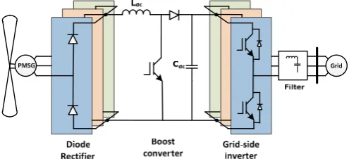
Small-scale wind turbines are mainly used to supply electricity to homes, farms, and small business in remote areas. They differ from their large-scale wind turbine in their rating, size, generator type, and the topology of the power electronics conversion system [5, 6]. For small-scale wind conversion system in the power ranges up to hundred kW, it is a trend to use a PMSG in industry applications especially for a directly driven wind turbine with benefits of size and weight reduction. As there is no reactive power needed, the conversion system is a simple 3-phase diode rectifier with dc-dc boost converter connected to 2-level full bridge Si IGBT PWM inverter as shown in Fig. 1 [6-9].
[image:1.595.308.556.600.713.2]Application of SiC devices in small-scale wind conversion system has been discussed in literature. In [10],designed a push-pull DC/DC converter achieved 93% peak efficiency developed for the HF isolation stage for a 1.3kW and operating frequency of 100kHz for PMSG-based wind turbines. However, no study has yet demonstrated the benefits of utilizing SiC in 2L-FB grid-side inverter based on 1200V SiC-MOSFETs module to improve the efficiency and achieve higher switching frequencies and power densities due to reducing the sizes of the passive elements and heatsink, neither optimized the heatsink design based on the wind speed distribution profile (i.e., in most works, the heatsink is designed based on the maximum operating output power). In
addition, this paper addresses the choice of the reference switching frequency value for SiC devices in this topology at this power level by some optimum compromise between the converter efficiency and volume. In this work, the performance analysis between SiC-MOSFETs and Si-IGBTs rated at 1200V blocking voltage in 10kW small-scale wind turbine is done based on a 2-level three phase grid-side inverter. Actually, the comparison is made between a three-phase bridge MOSFET power module rated at 1200V/20A (CCS020M12CM2 from CREE) and a three-phase bridge IGBT power module rated 1200V/25A (FS25R12W1T4_B11 from Infineon). This paper investigates the efficiency at different wind speed and a wide range of switching frequency and junction temperature in order to fully evaluate of SiC and Si devices. Here, the wind speed distribution profile is considered in the evaluation and design, and a critical discussion is presented.
This paper is organized as follows: description of the 2-level Full Bridge Inverter is presented in Section II; inverter power losses are modeled in section III; the inverter heatsink, DC-link and output filter are analyzed in Sections IV; the distribution and probability of wind speed are analyzed in Section V, the simulation and discussion are presented in section VI and, finally, the conclusion is discussed.
II. DESCRIPTION OF THE 2-LEVEL FULL BRIDGE INVERTER
Pulse width modulation voltage source inverter with two-level output voltage is one of the interesting candidates for the wind turbine. This topology is chosen to compare the influence of 1200V SiC devices based on a six-pack (three phase) module on the overall converter performance. As shown in Fig. 2., the wind turbine model under the maximum power point tracking is simplified by a current source connected in parallel with the DC link capacitor of the grid-side inverter. The input signal of the current source is [11]:
Iw=Pw,opt/Vdc. (1)
Where, Pw,opt is the optimal wind power and Vdc is the DC
link voltage of the converter.
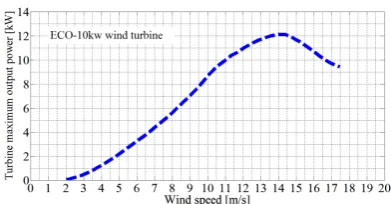
Here, the optimal output power of a 10kW commercial small-scale wind turbine as shown in Fig. 3 is considered [12].
In this study, the power rating of the inverter is 12kW, which is a representative figure for a commercial small-scale wind application and LC filter to minimize the output current harmonics.
III. INVERTER POWER LOSS MODELING
A. SiC Converter
The on-state voltage of SiC-based MOSFET and Schottky diode are calculated as follows [13]:
VS=ISRS,on. (2)
VD=VD,on+IDRD,on. (3)
Where ISand ID [A] are the conduction current through SiC
MOSFET and Schottky diode, respectively, RS,onand RD,on[Ω]
are on-state resistance for SiC MOSFET and Schottky diode,
respectively, and VD,on [V] is the Schottky diode on-state
voltage when ID=0.
The on-state resistances for SiC MOSFET switch as a function of the semiconductor junction temperature are as follows [14]:
RS,on=a2Tj2+a1Tj+a0 [mߗ]. (4)
Where a0, a1 and a2 are coefficients derived from MOSFET
on-state resistance information provided in the datasheet. The on-state voltage and resistance of Schottky diode depend on the junction temperature as follows [15]:
VD,on=αTj+VD0. (5)
RD,on= β Tj+RD0 [mߗ]. (6)
Where α, β, VD0 and RD,on are extrapolated from the
Schottky diode forward characteristic data provided by the manufacturer.
The values of conduction losses for SiC MOSFET and Schottky diode are calculated as follows [14]:
PS,con=I2(1/8+(1/3π)Mcosφ)×RS,on. (7)
PD,cond=I(1/2π-(1/8) Mcosφ)×VD,on+
I2(1/8-(1/3π)Mcosφ)×R
D,on. (8)
Where M is the modulation index, I [A] is the peak of
output phase current, φ [rad] is the current phase shift. The switching losses for SiC MOSFET switch is as follows [16]:
PS,sw=fsw(Vdc/Vdcref)kv((2b3/3π)I3+(b2/4)I2+(b1/π)I+(b0/2))×
(1+TCsw(Tj-Tjref))×10-6. (9)
Where b0, b1, b2 and b3 are coefficients derived from
MOSFET switching loss information provided in the
datasheet, kv is the exponent of voltage dependency
(MOSFET=1.5 [17]) and TCsw is the temperature coefficient
of switching losses (MOSFET =0, based on the fact that the change of switching energy losses of SiC MOSFET devices with temperature is negligible).
[image:2.595.325.521.62.164.2] [image:2.595.50.282.578.699.2]The tested SiC module has zero reverse recovery diode; therefore, the Schottky diode switching losses is neglected. Fig. 2. Two-Level Full Bride (2L-FB) inverter.
B. Si Converter
The on-state voltage of Si-based IGBT and power diode are calculated as follows [17]:
VS=VS,on+ISRS,on. (10)
VD=VD,on+IDRD,on. (11)
Where IS and ID are the conduction current through Si
IGBT and power diode, respectively, RS,onand RD,onare
on-state resistance for Si IGBT and power diode, respectively, and VS,on and VD,on are the Si IGBT and power diode on-state
voltage when IS=0 and ID=0 respectively.
The on-state voltage and resistance of Si IGBT switch depend on the semiconductor junction temperature as follows [18]:
VS,on=γTj+VS0. (12)
RS,on=a2Tj2+a1Tj+a0 [mߗ]. (13)
Where γ, VS0, a0, a1, and a2 are extracted from IGBT
forward characteristics information offered in the datasheet. The temperature dependency of on-state voltage and resistance of Si power diode are as follows [18]:
VD,on=αTj+VD0. (14)
RD,on= βTj+RD0 [mߗ]. (15)
Where α, β, VD0 and RD,on are extracted from Si power
diode forward characteristic information provided in the datasheet.
The conduction losses for Si IGBT and power diode are calculated as follows [17]:
PS,cond=I(1/2π+(1/8) Mcosφ)×VS,on+
I2(1/8+(1/3π)Mcosφ)×R
S,on. (16)
PD,cond=I(1/2π-(1/8) Mcosφ)×VD,on+
I2(1/8-(1/3π)Mcosφ)×R
D,on. (17)
The switching losses for Si IGBT switch and power diode are as follows [16]:
PS,sw=fsw(Vdc/Vdcref)kv((2b3/3π)I3+(b2/4)I2+(b1/π)I+(b0/2))×
(1+TCsw(Tj-Tjref))×10-6. (18)
PD,sw=fsw(Vdc/Vdcref)kv((2c3/2π)I3+(c2/4)I2+(c1/π)I+(c0/2))×
(1+TCsw(Tj-Tjref))×10-6. (19)
Where b0, b1, b2, and b3are constants derived from IGBT
switching losses data provided in the device datasheet, c0, c1,
c2, and c3are coefficients extracted from Si diode switching
losses, kv is the exponent of voltage dependency (IGBT=1
and Diode=1 [19])and TCsw is the temperature coefficient of
switching losses (IGBT=0.004 and Diode=0.006, which are derived from the energy switching losses information of Si IGBT and diode at different junction temperatures).
IV. INVERTER DESIGN AND VOLUME
A. Heat sink analysis
The heatsink thermal resistance can be calculated by the maximum power to be dissipated at a specific heatsink temperature as follow [20]:
Rha=(Th-Ta)/Pt. (20)
Where: Rha is the heatsink thermal resistance [W/°C], Th is
the reference heatsink temperature (equal to 60°C for PV and
wind energy applications), Ta is the ambient temperature
(chosen as 25°C), and Pt is the total semiconductor losses.
The thermal circuit for devices in 2-Level FB converter is shown in Fig. 4, where, Tj is the junction temperature, Tc is
the case temperature, Rjc is the junction to case thermal
resistance, and Rch is the case to heat sink thermal resistance.
The junction temperature for SiC MOSFET and Si IGBT devices can be calculated by (21) and (22), respectively:
Tj,MOSFET=PMOSFETRjc,MOSFET/6+Pt,SiCRch+Th. (21)
Tj,IGBT=PIGBTRjc,IGBT/6+Pt,SiRch+Th. (22)
Where, PMOSFET is the total loss of Si C MOSFET switches,
Pt,SiC is the total loss of the SiC MOSFET switches and SiC
Schottky diodes, PIGBT is the total loss of Si IGBT switches
and Pt,Si is the total loss of the Si IGBT switches and Si power
diodes.
The volume of heat sink based on natural and forced cooling is derived by curve fitting of commercial extruded heatsink volume. Based on heatsink thermal resistance, the heatsink volume for natural and forced convection cooling can be calculated by (23) and (24), respectively:
Volhs,Natural=45110Rha4-15400Rha3+109910Rha2- 47850Rha+8890 (23)
Volhs,Forced=117120Rha2-51950Rha+6670. (24)
B. DC-link analysis
The DC-link capacitor is to minimize the high switching frequency components of capacitor ripple current, as well as required for energy storage [21]. The DC-link capacitance by imposing a maximum current ripple to be carried by the capacitor and a peak-peak DC-link voltage ripple which is limited to 2% of the DC-link voltage is given as follows [22]:
Cdc=Icap,RMS/2π×fsw×ΔVdc(peak). (25)
The RMS capacitor ripple current is given by:
Icap,RMS =IN,RMS√[2M{√3/4π+cos2φ(√3/π-9M/16)}] (26)
Where M is the modulation index, IN is the output phase
current and φ is the current phase shift.
Power electronics conversion systems for the wind turbine are mainly based on a DC-link capacitor which occupies a significant part of the converter volume. The volume of the
[image:3.595.307.552.383.520.2]Fig. 4. Thermal circuit for Two-Level Full Bride (2L-FB) inverter.
DC-link capacitor at different switching frequencies is derived by a curve fitting of the actual design based on MKP film capacitor series as shown in Fig. 6, and given by (27). VolCdc=0.0898×10⁻⁶fsw2-0.0102fsw+431.78 (27)
C. Output filter analysis
The output filter of grid-connected inverter is to smooth the output ripple injected to the grid. The filter inductance of 2-Level three phase inverter is given as follows [23]:
Lf=Vdc/8fswΔIPP. (28)
Where Vdc [V] is the DC link voltage, fsw [Hz] is the
switching frequency and ΔIPP [A] is the peak to peak
switching ripple current in the filter inductance which can be limited to 10% of the output rated current.
The value of the filter inductor becomes significant for 2-level converters with power ratings of several kilowatts and above, thus, the inductor shares a valuable part of the converter volume. The inductor volume at different switching frequencies is derived based on the actual design and curve fitting of a standard C cut core as shown in Fig. 7 and given by (29).
VolL=0.02475×10⁻⁵fsw2-0.0308fsw+1527.852 (29)
The capacitor for LC filter does not contribute significantly to the converter volume and hence is ignored in this study.
V. WIND SPEED DISTRIBUTION
The wind speed distribution can be characterized by a Weibull distribution [24]:
φU=(k/C)(U/C)k-1exp[-(U/C)k]. (30)
Where, k [dimensionless] is the shape parameter and C
[m/s] is the scale parameter. The scale parameter C is related to the mean wind speed by the equation:
C=2Umean/ √π. (31)
[image:4.595.316.527.55.168.2]Umean [m/s] is the mean wind speed.
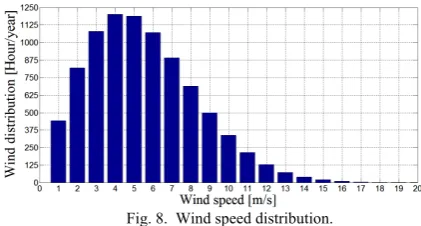
Fig. 8 shows the wind distribution in terms of hours per
year for a typical shape parameter k=2, and a mean wind
speed Umean=5.5m/s at a tower height of 15m for a chosen
site. It is clear that the wind speed distribution is high at low wind speeds; on the other hand, the wind speed distribution is low at high wind speeds.
The probability of the wind speed is the integration the Weibull distribution, and it is given as below:
Φ(U)=exp[-(U/C)k]. (32)
By considering wind turbine parameters of ECO-10kW [12], and as shown in Fig. 9, the turbine with rated speed of 11 m/s generates at full power only 4% of the time and at the minimum wind speed of 3m/s; the turbine generates power about 80% of the time.
VI. SIMULATION AND DISCUSSION
[image:4.595.55.286.85.221.2] [image:4.595.328.538.333.452.2]By simulating the converter over the range of wind speed from 3 to 17m/s at a switching frequency of 16kHz, which is the reference value of Si-IGBT devices used for this topology at this power level. The converter cell efficiency for both SiC-MOSFET and Si-IGBT devices is shown in Fig. 10. Over the whole rang, SiC devices show higher efficiency than that of Si, especially in the area where the wind distribution is high. Moreover, at the minimum wind speed operating range of 3m/s which has the chance of occurrence of 80%, SiC devices have higher efficiency by a value of 5.7% than that of Fig. 6. DC-link volume at different switching frequency
Fig. 7. Inductor volume at different switching frequency.
Fig. 8. Wind speed distribution.
Fig. 9. Wind speed probability.
[image:4.595.44.263.451.563.2] [image:4.595.311.537.597.698.2]Si devices. In addition, at the rated wind speed of 11m/s, the efficiency of SiC is about 99.3% compared to 97.8% for Si.
For grid-connected applications, by utilizing SiC devices solution instead of Si devices, the energy losses saving during a whole year is about 74.5% as shown in Fig. 11. By considering the existing UK infeed tariff for small-scale wind turbines (8.54p/kWh), the total money saving is around 45.7£/year. Even the initial price of SiC-MOSFET module is higher than that of Si-IGBT module, money saving by utilizing SiC devices will balance the cost after two years of operation.
When operating the converter at its maximum output power and a reference heatsink temperature of 60°C with a wide range of switch frequencies, the results in Fig. 12 show clearly that Si-IGBT devices can operate just on a narrow range of switching frequency due to a higher switching losses. In contrast with SiC devices, SiC works on a wider range of switching frequencies without significant loss of efficiency. Moreover, by increasing the switching frequency from 16kHz to 160kHz, the efficiency is dropped more quickly at the rate of 1.6% per 16kHz for Si and by a slower rate of 0.1% per 16kHz for SiC. This merit of SiC devices can lead to reduce the size and the cost of bulky filters and DC-link capacitor in 2-level converters without losing a significant amount of efficiency. However, increasing the switching frequency leads to a larger heatsink volume as a result of an increase in converter cell power losses.
To identify some optimum compromise between the converter efficiency and volume, the best switching frequency is selected in order to obtain minimum converter volumes as shown in Fig 13. It is clear that the heatsink and the output filter volumes have the main contribution to the total converter volume and the minimum volume is realized
at a switching frequency around 48kHz for the naturally cooled system. This value is considered to be the reference switching frequency for this topology at this power level. By switching SiC devices based converter at 48kHz, the cell efficiency is about 98.9% and still over the efficiency of Si devices switched at 16kHz by amount of 1.1%. In addition, this leads to reduce the output filter by a factor of 2.1 and the DC-link capacitor volume by 2.8 times and, therefore, higher power density.
By simulating the converter at the maximum wind turbine output power and converter switching frequency of 16kHz for both Si and SiC with different junction temperatures from 25°C to 150°C. The results show higher temperature capability of SiC devices when compared with Si devices. Moreover, as shown in Fig. 14, the SiC devices show 0.46% drop in efficiency which is much smaller than that of Si devices which show 1.3% drop in efficiency in the tested temperature range. In addition, it is obvious clearly that at the limited junction temperature of 150°C, the SiC devices have higher efficiency of 1.7% than that of Si devices.
Due to the SiC high-temperature capability, this can lead to reduce the converter cooling requirements compared with Si. By considering the heat sink reference temperature of 60°C and ambient temperature of 25°C, the required heat sink thermal resistance for SiC-based converter is 0.35 [°C/W] and 0.13 [°C/W] for Si converter. To realize the required heat sink volume, a commercial heatsink (195AB) based on natural and forced air flow convection is selected. The heatsink thermal resistance for SiC devices is attained by a natural convection and by a forced air flow cooled system for Si devices. The approximate volumes of heatsinks are 1863.9 cm3 (without fan volume) for Si and 1342.2cm3 for SiC.
Furthermore, SiC devices have the merit of very good thermal stability over a wide range of operation, this leads to Fig. 11. Energy and money saving by utilizing SiC devices in
[image:5.595.316.521.64.178.2]small-scale wind turbine inverter.
[image:5.595.63.278.191.324.2]Fig. 13.Heatsink volume, filter volume and total volume for SiC devices based inverter at different switching frequencies.
Fig. 12.Efficiency of SiC and Si versus switching frequency at the maximum output power and heatsink temperature of 60°C.
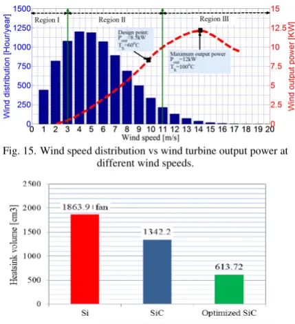
[image:5.595.59.269.609.714.2]increase the heatsink temperature without losing significant amount of power as shown in Fig. 14. Basically, the idea behind this is based on designing the heatsink at a reference temperature (i.e. 60°C) in region II (region of interest) as shown in Fig. 15, where the wind distribution is relatively high, and then pushing the heatsink temperature from 60°C to100°C at the maximum output power in region III where the wind distribution is relatively low. Moreover, by designing the heat sink at the wind output power of 8.5kW, efficiency of 99.3%, heatsink temperature of 60°C and ambient temperature of 25°C, the required thermal resistance
is 0.63 [°C/W] and the heatsink volume is 613.7cm3 based on
natural convection. Pushing the designed heatsink to operate at a temperature of 100°C at the maximum wind output power of 12kW leads to reduce the heatsink volume by a factor of 2.2 and thus higher power density with just 0.2% reduction in the converter efficiency for a short time per a year.
VII.CONCLUSION
This paper presented a performance benchmarking of Si-IGBTs and SiC-MOSFETs based inverter in a small-scale wind turbine. In particular, the benchmarking analysis of the devices with 1200V rating is performed based on 12kW 2-L Full Bridge grid-side inverter in 10kW small wind turbine. SiC devices show high efficiency than Si devices especially in the region of high wind speed distribution which leads to saving energy losses up to 75% at switching frequency of 16kHz. The reference switching frequency for SiC devices in this topology at this power level is determined around 48kHz based on the minimum converter volumes. Switching SiC devices at 48kHz allows reducing the output filter and DC-link capacitor sizes by a factor of 2.1 and 2.8 respectively. Due to the higher temperature capability of SiC devices, the
heatsink cooling requirements is reduced; the approximate heatsink volume reduction, not including cooling fans and accessories for Si devices, is about 1.4 times. In addition, combining a very good thermal stability of SiC devices and wind speed distribution profile allows increasing the heatsink temperature from 60°C to 100°C, thus leading to reduce the heatsink volume by a factor of 2.2 with just 0.2% reduction in the converter efficiency for a short time per a year. Even the initial cost of SiC-MOSFET power module is higher than Si IGBT power module, the higher efficiency of SiC devices, its higher switching frequency, and its higher thermal capability and thermal stability have reduced the cost of small wind power inverter. The cost reduction is due to saving energy losses, reducing the output filter, DC-link capacitor and heatsink sizes and the operation cost as well as. As part of future work, Practical tests which support the proposed analysis will be investigated.
ACKNOWLEDGMENT
The authors gratefully acknowledge the support of the Ministry of Higher Education, Libya, in carrying out this research.
REFERENCES
[1] Rabkowski, J., D. Peftitsis, and H.-P. Nee, Silicon carbide power transistors: A new era in power electronics is initiated. IEEE Industrial Electronics Magazine, 2012. 6(2): p. 17-26.
[2] Castellazzi, A., et al., SiC power MOSFETs performance, robustness and technology maturity. Microelectronics Reliability, 2016.
[3] Sintamarean, C., et al. Wide-band gap devices in PV systems-opportunities and challenges. in Power Electronics Conference (IPEC-Hiroshima 2014-ECCE-ASIA), 2014 International. 2014. IEEE.
[4] DiMarino, C.M., R. Burgos, and B. Dushan, High-temperature silicon carbide: characterization of state-of-the-art silicon carbide power transistors. IEEE Industrial Electronics Magazine, 2015. 9(3): p. 19-30.
[5] Whaley, D.M., Low-cost small-scale wind power generation. 2009, The University of Adelaide, Australia.
[6] Chub, A., et al. Grid integration issues of PMSG-based residential wind turbines. in Electric Power Quality and Supply Reliability Conference (PQ), 2014. 2014. IEEE.
[7] Song, S.-H., S.-i. Kang, and N.-K. Hahm. Implementation and control of grid connected AC-DC-AC power converter for variable speed wind energy conversion system. in Applied Power Electronics Conference and Exposition, 2003. APEC'03. Eighteenth Annual IEEE. 2003. IEEE. [8] Blaabjerg, F., M. Liserre, and K. Ma, Power electronics converters for wind turbine systems.
Industry Applications, IEEE Transactions on, 2012. 48(2): p. 708-719.
[9] Malinowski, M., et al., Optimized Energy-Conversion Systems for Small Wind Turbines: Renewable energy sources in modern distributed power generation systems. IEEE Power Electronics Magazine, 2015. 2(3): p. 16-30.
[10] Blinov, A., et al. Feasibility study of Si and SiC MOSFETs in high-gain DC/DC converter for renewable energy applications. in Proc. of IECON. 2013.
[11] Romlie, M.F., Impact of energy storage on the stability and transmission efficiency of a remote grid. 2014, University of Nottingham.
[12] Small wind turbines.[Online]. Available: http://www.small-windturbine.com
[13] Saridakis, S., E. Koutroulis, and F. Blaabjerg, Optimization of SiC-based H5 and Conergy-NPC transformerless PV inverters. Emerging and Selected Topics in Power Electronics, IEEE Journal of, 2015. 3(2): p. 555-567.
[14] Zhang, H. and L.M. Tolbert, Efficiency impact of silicon carbide power electronics for modern wind turbine full scale frequency converter. IEEE Transactions on Industrial Electronics, 2011. 58(1): p. 21-28.
[15] Selection Guide of SiC Schottky Diode in CCM PFC Applications. CPWR-AN05, REV, Cree, Inc., 4600 Silicon Drive, Durham, NC 27703.
[16] Nicolai, U. and A. Wintrich, Determining switching losses of SEMIKRON IGBT modules. SEMIKRON INTERNATIONAL GmbH, Nuremberg , Germany,Application Note AN 1403, 2014.
[17] Zhang, H., Electro-thermal modeling of SiC power electronic systems. Doctoral Dissertations, 2007: p. 201.
[18] Drofenik, U., G. Laimer, and J.W. Kolar. Theoretical converter power density limits for forced convection cooling. in Proceedings of the International PCIM Europe 2005 Conference. 2005. [19] Backlund, B., et al., Applying igbts. ABB, Lenzburg, Switzerland, Appl. Note 5SYA2053-01,
2007.
20] Seshasayee, N., Understanding thermal dissipation and design of a heatsink. Texas Instruments, Dallas, 2011.
[21] Kolar, J.W., et al. PWM converter power density barriers. in Power Conversion Conference-Nagoya, 2007. PCC'07. 2007. IEEE.
[22] Karanayil, B., V.G. Agelidis, and J. Pou. Evaluation of DC-link decoupling using electrolytic or polypropylene film capacitors in three-phase grid-connected photovoltaic inverters. in Industrial Electronics Society, IECON 2013-39th Annual Conference of the IEEE. 2013. IEEE. [23] Wang, T.C., et al. Output filter design for a grid-interconnected three-phase inverter. in Power
Electronics Specialist Conference, 2003. PESC'03. 2003 IEEE 34th Annual. 2003. IEEE. [24] Caretto, L., Use of probability distribution functions for wind. Mechanical Engineering, 2010.
[image:6.595.53.268.269.505.2]483.
Fig. 15.Wind speed distribution vs wind turbine output power at different wind speeds.