INSTRUCTION MANUAL
Lr[;1~©~®®
DOCll120-01
INSTRUCTION MANUAL .
TRS9200
TAPE READER/SPOOLER
For customer service contact ...
WARRANTY
Seller warrants that all goods furnished hereunder will at the time of shipment be free from defects in material and workmanship and will conform to Seller'S applicable specifications or, if appropriate to specifications accepted by Seller therefor. Seller's obligation hereunder shall be limited to, at Seller's option, either refunding the purchase price of, repairing or replacing, any products for which written notice of nonconformance hereunder is received by Seller within the Sellers Standard Warranty period for t!',e specific product; provided such nonconforming products are with Seller's prior authorization, returned F.O.B. Seller's plant at Buyer's expense. This warranty shall not apply to I
any products in other than their original condition, or to any products which Seller determines have, by Buyer or otherwise, been subjected to operating and/or environmental conditions in excess of the maximum values therefor in the applicable specifications or otherwise have been the subject of misuse, neglect, improper installation, repair, alteration or damage.
The foregoing warranties shall extend to Buyer, its successors, assigns, customers and ultimate users of his products. THESE WARRANTIES ARE EXPRESSLY IN LIEU OF ALL OTHER WARRANTIES WHETHER EX-PRESSED, IMPLIED OR STATUTORY, INCLUDING IMPLIED WARRANTIES OF MERCHANTABILITY OR FITNESS. IN NO EVENT WILL SELLER BE LIABLE FOR ANY SPECIAL, INCIDENTAL OR CONSEQUENTIAL DAMAGES.
NOTE: Warranty periods for specit.c products are as follows:
PRODUCT LENGTH OF WARRANTY PERIOD
- Tape Readers One (1) Year
- Punches One (1) Year
- Punch Mechanism Ninety (90) Days Switches
- Standard Switches One (1) Year Ninety (90) Days - 8000 Series
Electronic Packaging Products
-EECO 2D One (1) Year
One (1) Year -EECO 3D
Broadcast
- Video/Audio Tape Editing One (1) Year Computer Terminals
- D300/D400 VDU One (1) Year Any item not listed is not warranted by EECO.
June
1979
Paragraph
1-1
1-2
2-1
2-2
2-3
2-4
2-5
2-6
2-7
3-1
3-2
3-3
3-4
4-1
4-2
4-3
4-4
4-5
4-6
5-1
TABLE OF CONTENTS
Section I - General Description
Scope • . . • • • . . . • • • Equipm.ent Description
Section II - Installation and Operation
General
Installation •.
I.nterface
. .
. .
.
. .
.
.
.
Logic Modes.
.
.
.
.
Tape LQading Tape Splicing Operation •••
Section III - Functional Description General
Functional Des cription Reader
Spooler
.
,..
Section IV .,. Maintenance General
Preventi ve Maintenance Cleaning
Lubrication
.
.
,
Alignm.ent and Adjustm.ent Procedures Troubleshooting • . • • • • • • • • • • . •
Section V - Drawings and Parts Lists
.
.
.
.
.
.
.
General
.
.
.
. .
.
.
.
.
.
. . . .
.
. . .
.
.
.
.
.
. .
.
.
.
.
.
. .
.
1-1
1-1
2 -1
2 -1
2-1
2 .. 5
2-5
2-7
2-8
3-1
3-1
3-1
3-3
4 ... 1
4-1 4-1
4-2
4-3
4-13
Figure
1-1
2-1
2-2
2-32-4
2-5 3-1 4-1
4-2
4-3 4-4 4-5
4-6
4-74-8 4-9
Table
1-1
2 -1 4-14-2
LIST OF ILLUSTRATIONS
TRS9200 Reader /Spooler . . • . . . Input/ Output Signals • . . . Reader Interface Tirning Diagrarn
Recornrnended Reader/Spooler Interface Circuits Ta pe Loading . . . . . . • .
Tape Splice . . . • . Sirnp1ified Block Diagrarn Lubrica tion Points • . . . .
Control and Te st Point Locations Sprocket Wa veforrn . . • . . . . . . . Data Waveforrn . . . .
Sprocket Waveforrn Shift (Direction Change) Sprocket/Da ta Tirning (Negative Going) Sprocket/Data Tirning (Positive Going) Da ta /Sprocket Tirning Rela tionship
Stepper Motor Darnping Adjustrnent . . . .
LIST OF TABLES
Specifications . . . . Reader Logic Options . . . . Test Equipment and Special Tools Troubleshooting . . . .
,
.
.
.
iv 2-2
2-3
2-4
2-6
2-7 3-2
4-2
4-5 4-7 4-7
4-8 4-9
4-10
4-12
4-13
1-2
2-5 4-3A933
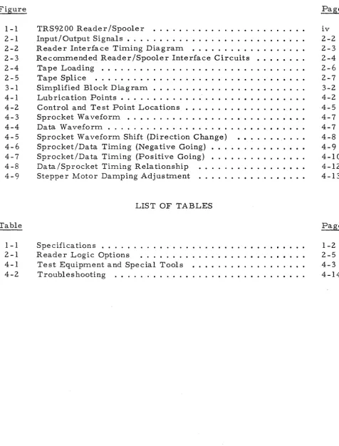
1-1. SCOPE.
SECTION I
GENERAL DESCRIPTION
The ITlanual contains operation and ITlaintenance inforITlation for the TRS9200 Tape Reader/Spooler (reader/spooler). This inforITlation includes general description, installation and operation procedures, functional descrip-tion, ITlaintenance procedures, engineering drawings, and parts lists.
1-2. EQUIPMENT DESCRIPTION.
The reader / spooler shown in figure I-I converts inforITlation in the forITl of hole patterns in perforated tape into electrical signals. Hole patterns conforITling to Electronic Industries Association standard RS-227-A, AITlerican National Standards X3. 18, AITlerican Standard Code for InforITlation Exchange X3.4, and all ITlajor COITlITlercial specifications are suitable. An adjustable tape guide perITlits reading of 5,
6,
7, or 8 -level tape. Tape supply and take-up reels 5 -1/4 inches in diaITleter have the capacity to hold take-up to 600 feet of tape. The reader/spooler is also capable of reading loops or strips of tape.,
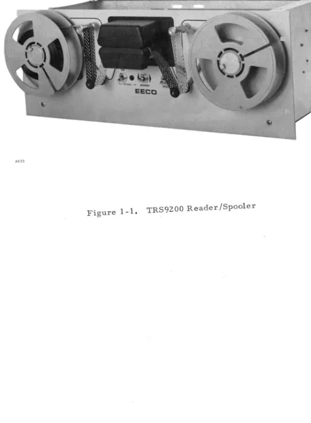
Parameter
Dimensions
Width
Height
5 -1/4 inch reels
Depth Weight Tape Material Thickness Tolerance Width/Levels
Tape Capacity
5-1/4 inch reel
Power Requirement
_ Fuse Requirement
Power Consumption
Maximum Typical
Peak Inrush Current
Logic Levels
Negative Logic
Normal Operating Temperatures at Room Ambient
Front of Read Head Back of Read Head Stepper Motor
Table 1-1. Specifications
Spe cification
19.00 inches
(48.26 centimeters)
7.00 inches
(17.8 centimeters) +2 inches for cables at bottom
7.00 inches
(17.8 centimeters)
15 pounds (6.8 kilograms)
Paper, aluminum-Mylar, paper-Mylar, or Mylar-aluminum
Up to 0.0045 inch (0.1143 millimeter)
Tape punched per EIA Standard RS-227 -A, ECMA, ANSI, or ISO
1.000 ±0.003 inch
(25.400 ±0.076 millimeters) 5, 6, 7, or standard 8 track plus sprocket
600 feet (182.88 meters)
115 ±100/0 Vac, 50-400 Hz
2 Amp Slo-Blo
120 watts 100 watts
4 amperes at 115 Vac
Logic 0 = +2.4 to +5.2 Vdc
at 400 {.LA
Logic 1 = 0.0 to +0.5 Vdc at 16 rnA
45°C 600
C 100 to 1350
C
Parameter
Reading Modes
Step (Pulse)
Pulse Width
Rate
Slew
Stop
Rewind
Stop Rewind
Data (8 channels)
Hole No Hole
READ CLOCK (Sprocket)
Hole No Hole
RUN STATUS
LOAD (Head Open) RU N (Head Closed)
DRIVE ACKNOW LEDGE
Step or Slew signal received
Step or Slew signal not received
READER READY
Ready
Not Ready
BROKEN TAPE
Tension arm in extreme downward position
Tension arm in normal operating position
Specification
Logic 1 input pulse synchronized with READER READY signal
35 fJ,s to 2 ms
o to 200 characters
(pulses) per second
Logic 1 input for duration of slew, 200 characters per second ±200/0
Logic 0
Logic 0 a't 5 rnA, 400 characters per second ±20%
Logic 1 at 100 {.LA
Logic 1 Logic 0
Logic 1 Logic 0
Logic 1 Logic 0
Logic 1 pulse 140 fJ,s ±300/0
Logic 0
Logic 1 when the reader is ready to accept an input drive command
Logic 0
Logic 1 indicates broken tape
[image:9.621.74.554.90.678.2]SECTION II
INSTALLA TION AND OPERATION
2 -1. GENERAL.
This section of the instruction manual contains installation and opera-tion informaopera-tion for the reader / spooler. Mounting, power and interface, tape loading, tape splicing, and operating instructions are provided. Refer to the Options section of this manual and/or interfacing equipment instruction manuals for special installation requirements.
2 -2. INSTALLATION.
The front panel is provided with mounting hole s for installation in a standard 19-inch RETMA equipment rack. Mounting slides may be provided as optional equipment. See outline dimension drawing 126701 in section V.
Apply power to the reader /spooler via the three-pin power connector J2. The power cord, three-wire Switchcraft part number P-2392 (EECO part number 346323-01) is supplied in the parts kit. Position the voltage select
switch S2, on the rear panel, for the voltage supplied.
When connecting the ac line cord to the line, be certain that the grounding pin is con-nected to a good ground source.
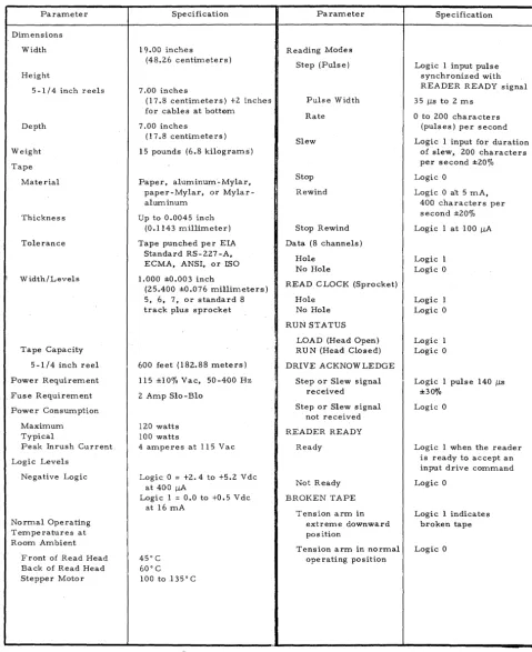
The data and control signals necessary for reader / spooler operation are shown in figure 2 -1. To interface with other equipment, fabricate appro-priate cables using size 22 AWG wire of necessary length not to exceed 10 feet. For noise immunity, use twisted pairs, terminated at both ends of the cable to the ground points •
2 - 3. Interface.
Jl J1
, -
h ~ ~DRIVE RIGHT +5VDC (REF)
4 1
DRIVE LEFT READER READY
5 6
SIGNAL GROUND RUN STATUS
25 7
L..o-~ 8 +24VDC (REF)
READ CLOCK (SPROCKET) 9
DRIVE ACKNOWLEDGE 10
DATA 1
11
DATA 2 READER 12
DATA 3 13
DATA 4 14
DATA 5 15
DATA 6 16
J2 DATA 7
~
"'"""
17
DATA 8
~
r-
18 +24VDC (REF)19
~
L
CHASSIS GROUND21
SIGNAL GROUND
' -...,.I 22
SIGNAL GROUND 23
SIGNAL GROUND 24
SIGNAL GROUND
25
-8461
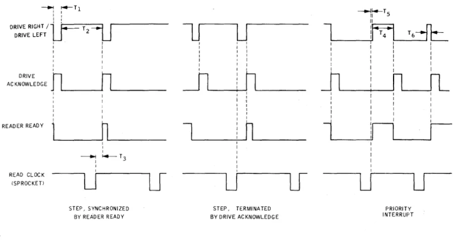
Figure 2-1. Input/Output Signals
Synchronize on the READER READY signal J1-6 by applying the step pulse only when READER READY is in the logic 1 state. READER READY goes to the logic 0 state when a step input is applied and returns to logic 1 typically 83 microseconds after the READ CLOCK (Sprocket) returns to logic 1 (t3). The minimum interval between step pulses is limited by the reader to 5
milli-seconds (t2) ..
[image:11.617.127.477.70.547.2]B422
~ ~Tl
I I I I
DRIVE RIGHT
Ilf=
TU
DRIVE LEFT 2
I I
I I
I I
I I
I
DRIVE
n
AC KNOWLEDGE
n
I
I
READER READY
n
I I I~ ~T3 I
I
READ CLOCK
LJ
Lf
(SPROCKET)
STEP, SYNCHRONIZED BY READ ER READY
lJ
IU
I I I
I I
:
I I
I I
I I
I
h
Jl
II I I I I I
l
n
I I I I
LJ
STEP, TERMINATED BY DRIVE ACKNOWLEDGE
lJ
----j\--
T 5 IIl
~'4~~!~
T6--fL
I I I
I I I
I i I
I I I
I I I
PRIORITY INTERRUPT
Figure 2 -2. Reader Interface Timing Diagram
For slew mode operation, hold DRIVE RIGHT or DRIVE LEFT at a logic 1 level for the duration of slewing. The repetition rate in the slew mode is limited by the reader. In the priority interrupt mode, an "interruption greater than 50 microseconds causes the reader to pause until another DRIVE input is received (t4). The reader continues to run at maximum speed if the DRIVE input is dropped for les s than 5
a
microseconds (t6). To stopon-character, remove the DRIVE input within 50 microseconds of the rising edge (hole-going condition) of the READ CLOCK (Sprocket) (t5).
Note
When switching from a DRIVE RIGHT input to a DRIVE left or vice versa in any mode, hold both inputs at logic
a
for a minimum of 50 microseconds.Sample the data after READ CLOCK (Sprocket) goes to the logic 1 level (hole condition). The READ CLOCK (Sprocket) may be delayed before
[image:12.620.73.539.118.356.2]t"Ij t-" ()Q ~ "i C1> N I W ~ C1> () 0
8
S
C1> :::s 0.. C1> 0.. ~N C1>
I P>
~ 0..
C1> "i
--
(J)ro
0 0 ... C1> 11 H :::s c-t" C1> 11"""
P> () C1> () t-" 11 () ~ t-" c-t" UlRECOMMENDED CUSTOMER DRIVE CIRCUIT
r---I
I
I
I
{ RUN STATUS READER SIGNALS DRIVE ACKNOWLEDGERIGHT 10K 10K t5V 10K 120 0.01
1
10K CD4030AEI
I
I
I
I
I
~~D
I
CD4030AE
I
0.01 507414
I
y,~~.:~.~
I
I
I CUSTOMER INPUTS{
::I:TEE:I::~T
I
~lill~LEF~T _ _ _ _ _ _ _ _ _ _ ~~I
~---~
120
- - - ,
I
READER OUTPUT CIRCUITSI
I
TYPICAL DATA CHANNELI
I
1
I
::i~::::::
I
I
~----
I
I
I
I
I
1 5N748&NREAD CLOCK (SPROCKET>
L __ ':" _ _ _ _ _ _ _ _ _ _
- _ jL . . - _ _ _ _ - _ _ _ _ -.J
r - - - ,
RECOMMENCED CUSTOMER INPUT CIRCUITI
I ..
I
1
SCHMITT TRIGGERI
I
.n - - -~.
~
:I
r,~
••~
""" -, I : -'M.-;.;'~
-11
0.01 SN74L04 CLOCK
: I
_____ J
I
I
NOISE FILTER
I
S:MI~ T:G£~-
II
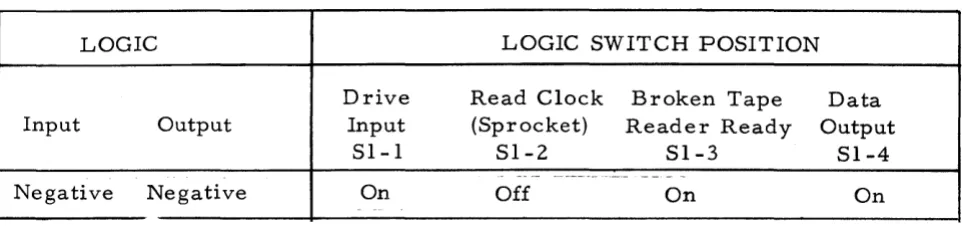
2 - 4. Log i c Mod e s.
Input andlor output logic m.odes m.ay be inverted by changing logic switch settings on the control printed circuit card. The logic m.ode options are listed in table 2 -1.
Table 2 -1. Reader Logic Options
LOGIC LOGIC SWITCH POSITION
Drive Read Clock Broken Tape Data Input Output Input (Sprocket) Reader Ready Output
SI-1 Sl-2 SI-3 SI-4
Negative Negative On Off On On
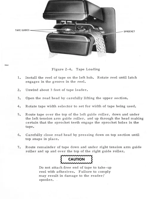
2-5. TAPE LOADING.
One inch, eight track tape has three rows of inform.ation holes on one side of the row of sprocket holes and five rows of inform.ation holes on the other side. Narrower tapes have three information holes on one side and fewer than five on the other. The tape is always installed with the three infor-mation holes nearest the front panel, that is, with the sprocket hole in the fourth row from the front panel.
The reel of tape to be read is normally installed on the left side of the reader
I
spooler. The free end of tape, which contains the leader followed by the beginning of information to be read, should leave the reel from the top. Tape unwinds when the reel is rotated clockwise. Forward travel of the tape is defined as left to right movement through the read head. [image:14.613.74.555.219.332.2]8460
TAPE GUIDES
-=========
~
SPROCKETFigure 2 -4. Tape Loading
1. Install the reel of tape on the left hub. Rotate reel until latch
engages in the groove in the reel.
2. Unwind about 3 feet of tape leader.
3. Open the read head by carefully lifting the upper section. 4. Rotate tape width selecto~ to set for width of tape being used. 5. Route tape over the top of the left guide roller, down and under
the left tension arrn guide roller, and up through the head making
certain that the sprocket teeth engage the sprocket holes in the tape.
6. Carefully close read head by pressing down on top section until top snaps in place.
7. Route remainder of tape down and under right tension arm guide
roller and up and over the top of the right guide roller.
Do not attach free end of tape to take - up reel with adhesives. Failure to comply
may result in damage to the reader /
[image:15.611.47.540.89.753.2]8. Attach tape leader to take-up reel by inserting free end of tape into 'slot in reel. Tape ITlust pas s over top of reel for clockwise
rotation.
9.
Manually rotate each reel to take up tape slack.2 -
6.
TAPE SPLICING.When neces sary to splice punched tape, a butt splice is recoITlITlended. A butt splice is ITlade by placing the square-cut ends of the tape together with-out overlapping (see figure 2 - 5). Care should be taken to ITlaintain the proper distance between holes. The hole spacing should be O. 100 ±O. 001 inches.
Splicing can best be accoITlplished by use of a cOITlITlercial punched tape splicer such as ITlanufactured by the Data-Link Corp. There should also be no lateral shift of the tape ends. Apply contact adhesive splicing ITlaterial such as silver Scotch tape No. 852 to the top side of the punched tape so that it will be away froITl the phototransistor array and sprocket wheel. Pre-punched splices are
also available froITl several sources. Be certain the splicing ITlaterial ends between holes. TriITl the splicing ITlaterial evenly at the edges of the tape. Do not use transparent splicing ITlaterial on butt spliced tape.
BUTTED TAPE ENDS
o
o
o
o
o
o
o
o
o
A158 SPLICING MATERIAL
2-7. OPERATION.
Operator controls and an indicator are located on the front panel (see figure 1-1). The operation and functions of the controls and indicator are
des-cribed below.
POWER switch POWER indicator
REWIND switch
SPOOL/LOOP switch
Applies power to the reader / spooler. A LED indicator that lights when 115 Vac power is applied to the reader / spooler and internal dc power is available.
A three-position momentary toggle switch to wind the tape at 400 chara.cters per second on either reel. In the left rewind position (~ ), tape travels from right to left through the read head and winds on the left reel. Tape is
wound on the right reel in the right rewind position ( ~). The center position is the normal speed run position.
A two-position toggle switch. When set to SPOOL for operation using reels of tape, the spooler motors are active and the
BROKEN TA,PE output signal is also Ci '::ive.
The LOOP position is for operation u~:.·<!~
loops or strips of tape. In the LOOP r.':)t.
3-1. GENERAL.
SECTION III
FUNCTIONAL DESCRIPTION
This section describes the operation of the reader / spooler on a func-tional basis. The description is in the form. of a block diagram. explanation of the unit.
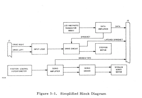
3-2. FUNCTIONAL DESCRIPTION.
A sim.plified block diagram. of the reader/spooler is shown in figure 3-1. Note that the unit is divided into two sections, reader and spooler, \~-ith
no electrical connection between sections.
3-3. Reader.
The reader section of the reader / spooler is a photoelectric perforated tape ,reader. The perforated tape, driven by the stepper m.otor, passes be-tween a light-em.itting diode (LED) array and a phototransistor array located in the read head. Infrared light from. the LED array pas ses through holes in the tape to cause the phototransistors to conduct. Outputs of the phototransis-tor array are applied to the data am.plifier where they are amplified, \x/ave
shaped, and applied to exclusive OR gates for logic level selection. Eight data signals, corresponding to eight tracks of tape holes, and several inter-face signal s are available at the input/ output connector.
External control signals are applied through the input/ output connector to the input logic circuit. The input logic circuit provides motor drive logic control signals. These logic signals are amplified by the m.otor drive circuit to the power level necessary to activate the stepper motor. As the stepper motor drives the tape to a new row of holes, the sprocket hole initiates several
control signals. Status signals are available at the input/output connector to be used to control operation of the reader.
The LED array consists of light-emitting diodes arranged in a nine-diode array. The LED's transmit infrared light through holes in the perforated tape to be sensed by nine similarly arranged phototransistors. Current
Jl
r---.
LED AND PHOTO DATA
DATA TRANSISTOR
AMPLIFIER ARRAY
SPROCKET
I
Jl
i
LATCHED SPROCKET----..,
~
DRIVE RIGHT
DRIVE CIRCUIT STEPPER
DRIVE LEFT INPUT LOGIC MOTOR
~
BROKEN TAPE
I
"'"
.-'" SPOOLER
POSITION CONTROL SERVO SERVO
SERVO
POTENTIOMETER AMPLIFIER DRIVER
MOTOR 452B
Figure 3 -1. Simplified Block Diagram
The data amplifier consists of eight voltage comparators, each con-nected to an exclusive OR gate. A voltage comparator compares the output of a phototransistor to a reference voltage. When the voltage from the photo-transistor is less than the reference voltage (hole condition), the comparator output is low. When the voltage from the phototransistor is greater than the reference voltage (no-hole condition), the comparator output is high.
Each comparator output is applied to one input of an exclusive OR gate. The other input to an exclusive OR gate is selected by an internal switch and can be either ground or +5 volts. A ground (switch closed) results in a low output from an exclusive OR gate when a hole is present. +5 volts (switch open) results in a high output when a hole is present.
[image:19.623.65.554.49.387.2]The stepper motor is a four-phase motor that drives the sprocket. The sprocket engages the sprocket holes in the tape and propels the tape in the direction controlled by the externally supplied control signals. The
direction of rotation of the motor is determined by the sequence of energizing adjacent pairs of motor windings.
3-4. Spooler.
The spooler consists of two identical and separate right and left servo control circuits. Each circuit drives a tape reel in response to a control potentiometer. This closed-loop proportional system is balanced with the servo motors running or stopped to maintain the tape tension arms near the center (neutral) position. The spooler is disabled when the SPOOL/LOOP switch is in LOOP.
+20 volts is applied to the control potentiometers which are mechanically positioned by the tape tension arms. Movement of the tape tension arms
changes the voltage from the control potentiometers which is applied to the servo electronics. Voltage from the potentiometers change s with tape speed.
The servo electronics amplifies the voltages from the control poten-tiometers and determines the required direction and speed of the respective spooler motor. A lead-lag compensator momentarily boosts the amplifier output voltage for rapid servo motor response and system stability.
4-1.
SECTION IV MAINTENANCE
WARNING
I
Hazardous voltages are present in this equipment when power is connected. Use caution to avoid electrical
shock.
GENERAL.
This section contains information for maintaining the reader / spooler. The instructions include preventive maintenance, alignments and adjustments, and troubleshooting.
4-2. PREVENTIVE MAINTENANCE.
Preventive maintenance consists of cleaning and lubrication. When performed at regular intervals, reader / spooler breakdown may be prevented and optimum performance ensured.
4-3. Cleaning.
The glass surfaces of the read head must be cleaned to prevent exces-sive accumulation of dirt from causing misreading of tape. To clean the read head, perform the following procedure.
Do not use sharp tools or volatile solvents. Avoid excessive pressure in glass.
Fail-ure to comply may result in damage to equipment.
1. Open head by carefully pulling up top section.
2. With a dry cotton swab, wipe the two glass surfaces and surround-ing area of head. If glas s cannot be cleaned thoroughly with a dry cotton swab, proceed with the following steps.
3. Prepare a cleaning solution of water and mild liquid detergent.
4. Wipe glass surfaces with clean cotton swab moistened with clean-ing solution. Use solution sparclean-ingly and do not saturate area. 5. Rinse area with clean cotton swab moistened with clean water.
7. Inspect glass surfaces for cleanliness ITlaking certain that no
resi-due is present. If further cleaning is required, repeat steps 3
through 7 until glass is thoroughly clean.
8. Close read head by pressing down on top section until top snaps in
place.
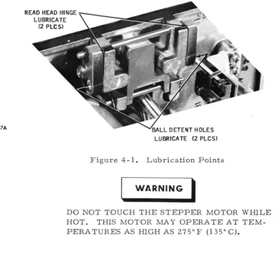
4-4. Lubrication.
Lubrication is required on the read head cove r hinge and ball detent
holes. A sITlall aITlount of Dow Corning 33 lubricant ITlay be used in the loca-tions pointed out in figure 4-1.
587A
READ HEAD HINGE LUBRICATE
(2 PLCS)
LL DETENT HOLES LUBRICATE (2 PLCS)
Figure 4-1. Lubrication Points
WARNING
I
DO NOT TOUCH THE STEPPER MOTOR WHILE
HOT. THIS MOTOR MAY OPERATE A T
[image:23.613.64.465.305.681.2]4-5. A.LIGNMENT AND ADJUSTMENT PROCEDURES.
All alignments and adjustments, both mechanical and electrical, are carried out initially at the factory. Readjustments should not normally be necessary; however, due to wear or replacement of parts and components,
some readjustments may be required.
Positive input/output logic is used in these procedures. The positive logic levels are:
Logic 0
=
0.0 to +0.4 Vdc at 16 rnilliamps (sink) Logic 1=
+2.4 to +5.2 Vdc at 400 milliamps (source)For a reader/spooler using negative logic, interchange the two logic levels. Unless otherwise specified, all parameter tolerances are ±lO%.
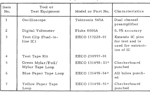
Test equiprnent and special tools required to perform alignment and adjustments are listed in table 4-1. Equivalent test equipment and tools may be substituted.
Table 4-1. Test Equipment and Special Tools
Item Tool or
No. Test Equipment Model or Part No. Characteristics
1 Oscilloscope Tektronix 545A Dual channel
preamplifier 2 Digital Voltmeter Fluke 8000A O. 50/0 accuracy 3 Test Clip (Dual-in- EECO 117228-01 Extends IC pins
line IC) for test and is
used for extract-ion of IC
4 Test Tape Kit EECO 230997-01
5 Green Mylar /Foil/ EECO 131498-11>:< Checkerboard
Mylar Tape Loop punched
6 Blue Paper Tape Loop EECO 131498 ~54>:< All hole s punch-ed
7 Yellow Paper Tape EECO 131498-91>:< Checkerboard
Loop punched
[image:24.615.68.552.398.694.2]1. Spooler Servo Control PotentioITleter AlignITlent
Note
No tape or reels a re required for this adjustITlent.
a. Connect power to the reader/spooler.
b. Set POWER switch up (on) and SPOOL/LOOP switch to SPOOL.
c. Manually ITlove the left tape arITl approxiITlately 1/2 inch away froITl the rubber stopper and verify that the left
spooler ITlotor rotates in the correct direction (counter-clockwise). Continue to raise tape arITl and note servo ITlotor slows to a stop in a null position. As tape arITl is
raised further, the ITlotor will rotate in opposite direction· (clockwise). If ITlotor rotates in the correct direction proceed to step d.
d. Manually lower left tape arITl until ITlotor stops. Tape arITl should be 0.25 ± 0.1 inch from lower rubber stopper.
If the position of the tape arm is not within specification, re-adjust by loosening the set screw and ITlove the tape
arITl to the correct position. Retighten the set screw, then relea s e the tape a rITl. Repeats tep s c and d to ve r ify that the adjustITlent has been perforITled properly.
e. Repeat steps c and d for the right tape arITl except the rigr ... t ITlotor should rotate clockwise when the arITl is first raised.
2. LED Current and Phototransistor Output AdjustITlents a. Power
(1) Set the reader/spooler power switch to ON. (2) Verify that power LED is on.
(3) Using the digital ITlultimeter, verify that the voltage at the printed circuit board (PCB) connector Jl pin 1
J6
6637
Dr}~
JS
~
Q34R132
[][][][][][][]
[]
IC3 IC4 ICS IC6 IC7 ICB IC9
000
TP13 rpl0 TP12 [ ]
a~~~~~[J
[][][][][]
IC2
RPl
OTP1S
~ REWIND R133
R1l3
LED (I) SLEW
CH 1 CH 2
CH 3 CH 4
CH S
CH 6
CH 7 CH B
SPKT
IC16 IC17 IC18 IC19 IC20
QrR40[]
~ ~
TP 0 CH 1
@ CH2 @ CH3 <9 CH4
o CHS
@ CH6
[][]
~ ~~~J4 . , (!) SPKT
l:
'.J"
SIGNAL GROUNDIC24 IC2S _~" J
~l; I - I -I
Jl
Figure 4-2. Control and Test Point Locations (4) Verify that the voltage at fuse F2 is +22.0 to
+26.0 Vdc.
b. LED Current Adjustment
(1) Place the reader / spooler in the Loop Mode.
WARNING
I
MOTOR MAY BE HOT
(2) Load the green te st tape (P
IN
131498 -11) into the read head. Be sure the sprocket teeth are engaged and a character is lined up to be read by photo array. If the character does not align with the photo array when power is applied to the unit, loosen the threesynclamps which secure the motor to the mounting pIa te a nd rotate the body of the motor until the character and the photo array are aligned. Tighten the synclamps.
[image:26.612.61.500.114.756.2]Note
If no computer or test box is available, this may be accom-plished by jumpering as follows: Positive Logic Unit - J1 pin 4
(DRIVE RIGHT) to J1 pin
25
(SIGNAL COMMON) Negative Logic Unit - J1 pin 4
(DRIVE RIGHT) to J1 pin 1
(+5VDC)
(4) If the reader/spooler operates satisfactorily, go to paragraph c.
(5) If the reader / spooler fails to operate, adjust the LED potentiometer (R133) on the printed circuit board for 1. 6 Vdc to 1. 8 Vdc at test point TP15.
(Use the digital multimeter. )
Note
If motor fails to run, continue with paragraph c.
c. Photo Transistor Adjustment
(1) Load the blue test (P/N 131498-54) into the read head. (2) Operate the reader/spooler in the slew right mode.
3.0VDC 2.4VDC (MIN)
O.7VDC (MAX) O.4VDC (MAX) O.OVDC 6814
B815 3.0VDC
O.4VDC (MAX) O.OVDC (REF)
(4) Stabilize and trigger the scope at about +1.0 Vdc. (5) Adjust the PCB sprocket potentiometer (Rl13) until
the no-hole portion of the waveform is at +3.0 Vdc. (See figure 4-3.) Keep the baseline below +0.4 Vdc and any dips above +2.4 Vdc. If +3.
a
Vdc cannot bereached with the sprocket potentiometer, adjust the LED potentiometer (R133) slightly until +3.0 Vdc can be reached.
---(6)
Figure 4-3. Sprocket Waveform
Move the scope probe to each of the eight PCB data test points (TPI-TP8) and adjust the eight corres-pending data channel potentiometers (RI05 through Rl12) for +3.
a
Vdc at the no-hole portion of the wa veform. (See figure 4-4. )HOLE
- - - -
[image:28.615.63.540.98.691.2]LOGIC 1 DRIVE ACK~OWLEDGE
LOGIC 0 LOGIC 1 SPROCKET
LOGIC 0 8816
d. Stepper Motor Rotational Alignment
WARNING
I
STEPPER MOTOR MAY BE EXTREMELY HOT!. DO NOT TOUCH MOTOR WITH BARE HA.NDS.
(1) Load the green test tape (P /N 131498 -11) into the read head.
(2) Set the scope to alternate mode, external trigger. (3) Place the channel A scope probe to test point TP12
or connector Jl pin 10 (DRIVE-ACKNOWLEDGE). Trigger the scope on Jl pin 10.
(4) Place the channel B scope probe to the PCB test point TP9 (raw sprocket).
(5) Operate the reader/spooler in slew mode.
(6) While observing channel B, reverse the tape direct-ion. Verify that the shift in position of the positive-going leading edge of the waveform does not exceed 200 microseconds. (See figure 4-5.). If the shift is less than 200 microseconds, go to paragraph e.
~--200USEC
[image:29.617.68.542.59.735.2]SPROCKET
DATA
8817
(7) If the waveform shift exceeds 200 microseconds: (a) Loosen the three syn-clamp screws which secure
the stepper motor to its mounting plate.
(b) Rotate the body of the motor while reversing the tape direction until the shift is less than 200 microseconds.
(c) Retighten the three screws. (d) Repeat paragraph d(6). e. Data Channel
LOGIC 1
LOGIC 0
LOGIC 1
LOGIC 0
(1) Load the blue test tape (P/N 131498-54) into the read head.
(2) Ope ra te the reader / spooler in the slew right mode.
(3) P~_ace _t~~_channel A scope probe at the PCB connector
J1 pin
9
(sprocket). Trigger scope on external negat-ive at J1 pin9.
(4) Place the channel B scope probe on each of the eight data test points (PCB connector Jl pins 11 - 18) and
check for the waveform of figure 4- 6.
l
I.
-I
lOOUSEC (MIN)Ij
[image:30.613.79.532.78.704.2]DATA
SPROCKET
B818
LOGIC 1
LOGIC 0 LOGIC 1
LOGIC 0
(5) If any data negative excursion is less than 100 micro-seconds after the sprocket negative excursion, adjust the corresponding potentiometer (RIDS through R112) slightly to obtain 100 micorseconds.
(6) Move the channel A s cope probe to the data 1 te s t point (JI pin 1). Trigger the scope on external positive at pin 1.
(7) Move channel B scope lead to the sprocket test point (JI pin
9).
(8) Check for the waveform of figure 4-7. If the positive sprocket excursion is less than 100 microseconds after the data positive excursion, adjust the data potentiometer (RIDS) slightly to obtain 100 micro-seconds.
(9) Move the channel A scope probe and trigger to each of the other seven data test points (JI pin 2-8) and observe the waveform of figure 4-7. Again, if the sprocket positive excursion is less than 100 micro-seconds, adjust the corresponding data potentiom.eter (RI06 - R112) to obtain 100 microseconds.
J
I.
-I
lOOUSEC (MIN)•
Figure 4-7. Sprocket/Da ta Timing (Positive Going)
£. Error-Free Check
If an EECO test box (P/N SKD2907) or proper computer test program is available, use the yellow test tape
(P /N 131498 - 91) to check the error-free operation.
Note
The reader / spooler may not operate error-free using tapes with an opacity equal to or greater than the yellow test tape (per ANSI X 3.29 - 1971). If the reader/spooler makes reading errors after alignment, consult the factory.
3. Data/Sprocket Timing
a. Load the all holes tapes loop (item 6 of table 4-1) and operate in the slew mode.
b. Moni tor ea ch da ta phototrans istor output te st point (TP 1 through TP8) relative to the sprocket phototransistor output at TP9 for the characteristics shown. in figure 4-8. SynchroTnize the oscilloscope with the sprocket signal.
c. If 6 t l of 6t2 is less than 100 microseconds, increase sprocket (SPKT) phototransistor output voltage by adjust-ing potentiometer Rl13. See paragraph 2. c. (5).
d. Remove the tape from the read head and verify that TP9 is less than +0.4 Vdc.
4. Slew Speed Adj ustment
a. Monitor the motor clock pulses at TP12 on the printed circuit card while opera ting the reader / spooler in the slew mode.
3.0 VOLTS MIN. (NO HOLE) - - -
-SPROCKET WAVEFORM
o. 4 VOLTS MAX. (H OLE) - - -
-3.0 VOLTS MI N. (NO HOLE) - - -
-o. 4 VOLTS MAX. (HOLE) - - - DATA WA~EFORM
A871
Figure 4-8. Data/Sprocket Timing Relationship 5. Stepper Motor Damping Adjustment
a. Monitor the sprocket waveform at TP9 with an oscilloscope.
b. Step the reader at various speeds to find a resonant condition. At resonance, the oscilloscope will display a waveform similar to the one shown in figure 4-9A. c. ,Adjust rheostat RSI until a clean sprocket waveform is
obtained as shown in figure 4-9B.
[image:33.613.71.527.74.740.2]AI035
4-6.
A. RESONANCE
[image:34.615.63.528.72.628.2]B. RSI ADJUSTED TO REMOVE RESONANCE
Figure
4-9.
Stepper Motor Damping Adjustment6.
Rewind Speed Adjustmenta. Monitor the motor clock pulses at TP12 on the printed circuit card while operating the reader/spooler in the rewind mode.
b. Adjust potentioITleter R137 until the tiITle between the leading edges of pulses is 2.5 ITlilliseconds.
TROUBLESHOOTING.
Item
1
2
3
Observe standard CMOS handling procedures where applicable.
Note
Logic levels must be measured using an oscillosc,?pe or digital voltmeter, not a multirneter. Access to integrated circuit pins is gained by attaching the dual-in-line IC test clip to the integrated circuit package. The IC test clip is also used to remove IC packages from the printed circuit board.
Table 4-2. Troubleshooting
Symptom Remedy
Stepper Motor does not a. Check input power and fuse. step. b. Thread tape correctly. Refer
to tape loading procedure in section II.
c. Check RUN STATUS signal (Jl-7) logic 0 to run.
d. Verify proper input signals. e. Check logic level switches for
desired logic option.
£. Check power supply voltages. See schema.tic 126706.
g. Troubleshoot control card.
Stepper 11otor steps in a. Check DRIVE RIGHT and DRIVE one, direction only. LEFT signal levels. J1-4 at
logic 1 for the right tape travel. J 1- 5 at logic 1 for left tape tra vel with the rema ining input at logic O.
b. Troubleshoot input logic circuit. Motor steps erratically. a. Perform alignment and
adjust-ITlent procedure in section IV.
[image:35.617.69.566.185.708.2]Item 4
5
6
7
8
9
10
Table 4-2. Troubleshooting (Continued)
SYlnptom
Incorrect reading ra teo
Tape chatters or flutters and does not drive
smoothly. No data output.
Erroneous data output.
Both spooler motors inoperative.
One spooler motor inoperative.
Incorrect rewind speed.
Remedy
C.heck slew speed adjustment proced-ure in section IV.
Check stepper motor damping ad-justment procedure in section IV.
a. Verify proper LED current. Refer to adjustment procedure
in section IV.
b. Check logic level switch. Refer to section II.
c. Check phototransistor outputs TP 1 through TP8.
a. Clean read head. See cleaning procedure in section IV.
b. Check individual phototransistor outputs at TPI through TP8. a. Check that SPOOL/LOOP
switch is in SPOOL.
b. Verify that tape tension arms are in correct position.
c. Check spooler control potent-iometer adjustment procedure in section IV.
d. Check dc power supply voltages. Troubleshoot respective servo
circuit.
a. Check rewind speed adjustment in section IV.
[image:36.621.76.559.98.685.2]SECTION V
DRAWINGS AND PAR TS LIST
5-1. GENERAL.
This section contains parts lists and those asseITlbly and sche-ITlatic drawings necessary for ITlaintenance and operation of the EECO
Mod-el TRS9200 Tape Reader /Spooler as ITlodified by EECO specification
230438-01. The parts lists are grouped together and followed by the asseITl-blyand schematic drawings arranged in nUITlerical order.
Description Parts List A sseITlb1y ScheITla tic Tape Reader /Spoo1er 230438-01 126702 127136
Front Panel Ass emb1y 126808-02 126808 Read Head AsseITlb1y 127124-01 127124
Control Card PCB 126706-02 126706 126706 (Sheet 1) (Sheet 2, 3) Resistor Cable Assembly 127166-01 127166 127166
Parts Kit 129162-01
F-:1FCTRONIt. ENGINEERING CO. cone tDENT 91525
JfSCR. P(~ ASSy,RORISPLR CNTL
ENGNG ow; ~ 126706 eco PEND CONTR NO.
RFF LN Ii
01V
R~OO U/M LEVEL PART NO. OR tOENT NO. e
e
REV LTR veNDOR P'_T NO. oeSCRIPTION 1.24 J.37 130 131 t28 5 129 'B 20 14 15 19 18 17 21 J 6 ?1 23 22 11 25 ?f-1<\4.'. l0 I .? 1
1:\ 7
! '~-l
138
139 105 l'H
1 I)E, 11)8 US lAO lCl2 100 109 <; 8 93 Q4 PO
2o()OO EA 2.0000 EA
~s.ooo fA H~OOO EA
18~OOO EA
~EF EA
1,000 EA
~!==F EA
REF EA 11()OO EA 7.l'lQO EA
2, '.'00 EA 11. :000 EA
1.)00 EA
1 ~'';OO EA IlttOO EA
1.000 EA
2.'000 E~ lllOOO EA
1.:')00 EA
1.000 EA
1.000 EA 4.000 EA 1,000 EA
4.000 FA AIR EA
AIR EA
2.000 fA
1.01)0 EA
1..000 fA
1.00(; ~A
3.000 EA
3.000 EA
1.000 fA
1.000 EA
1.000 fA l,OOO EA
1.000 EA
1.000 EA
1,000 fA
1.000 fA
1.000 EA 5.000 fA 10.000 fA 17.01)0 EA 8.000 EA l~ ,000 EA
05 110642-03
05 110642 .. 04
05 110659-02
05 110662-02
05 110664-04
04 12.6706
04 126707-01
04 126109
04 126710
04 126830-84
()4 304061 .. 25
04 .304061 .. 33
07 304rf;1-37
07 3041",1"-'72 07 30~q:'1"'30
05 304.,;; 1..,38
05 3044H-47
04 3048~0 .. 05
04 3048!J0 .. 17
04 304650-21
07 3Q4951 .. 10.,
04 304951-15
04 304951.22
04 304951 ... 28.
04 304951-32
04 3060]9.03
07 306351-02
05 311006-02
04 311035-01
04 'H 1 035 ... 03
04 .H 1035-04
04 311035-07
04 311035 .. 08 04 311035-11 04 311035.13
04 311035-22
04 311035-23
04 311035.24
04 31103S'!"37
0/. 311035.47
04 31103,.48
07 .311182-02
04 311273-05 04 311273-06
04 312202·01. 04 ~1?Z02-02
04 322049-02
)( e
x c
X B X FX 0
X R.
X G
X A X C
X 0
X 0
X 0
X D
X 0
X B
X 9
X B
X D X D X n
x
Lx L
X L
,)( L )( L )( E X C X F X N )( N
X N
X N X N X N X III
X N
)( '"
X N
X N X '"
X N
. X H
X G X G X F X F
X C
.. -,._---'" . .
-~-MS51957-13 SeR, ~AN HD 4-40Xl/4
MS51951.14 SeR, PAN HD 4-40)(5/16
M.S.1!3'U.l0 WASHER. INT TOOTH '114 _ ...
MS1'l" •• OS WASHER,FI..ATt4
NAS6'U.C4 NtJT,HEX 4-40 NC SM
EE.C1L .... _, __ · _._""'_'.' ~8. A5..SV.ROlllSPLR Ctl/.TL
EECO PCB,eONT CARD,RnRISPLR
eEeO ATP,CONTROL CARD
EEto ., -.'''_. _ _ _ . ..A.t.c .. ao.a I SP U C NTI.. CAiD
EECO. LG eXT RunED HEAT S!NK
CK058XI02K CAP,.lOOOPF 200'1+-10'
SEE. s.t.O. ,-_ .. _ ... -CA.P •• 4.700PF 100'1 .-1.0t
CK05BXI03K CAP ••• OlUF 100V 10~
CK06BXI04K CAP., .1UF 100V lot
DM.15.!!l.OlL ____ ~ • ..I 100PF 500V 51 DM-1'-221J CAP., 220PF SOOV 5_ OM.15-411J CAP •• ~70PF 500V 5'
192PlQ2.9.2.. __ ....:.._; ... _.~_CA2... t,~0010UF 200V 101
192PI0392 CAP.,.OlOUF 200V 101
192P22392 CAP ••• 022RF lOOV 101
CSR1.3D22bK. .... __ . ___ .cAP- • .t.22UF 15V 10 CS~13EI06K CAP •• 10UF lOV 101
CSR13P474K CAP ••• 47UF 35V 101 .
CSR13'Y.75.K_., . .. ..c..Al ... , 4.7UF .35'1 101
CSR13F226K CAP., 22UF 35V 101·
NO. 92X.250W TAPE,THERMO SETTING
340 .CMPO,SILICONE HTSNK
0110277 LATCH,SPRING CONN
ABce
09-18-5121 CONN,12 pos WFR
09.18.'!!O.6l... .... __ .... __ :.C'ONNt6 POS HOR.
09.18-5960 CONN,6 POS HOR
02.09-2118 TeR~.PIN 18-22 AWG 02.09~111a _ ~ER~. SKT 1a-22 AWG 09.18.5069 CONN,6 POS H~R
09-18-5031 CONN,3 POS HOR
09.18-5062 CONN,6 POS HOR
09-18-5064 CONN.6 POS HOR
03-09-2032 CONN.3 POS PLUG
03'!09-1033. . .... CONN, 3 pos RCPT
09-18-5035 CONN,3 POS HOR
09-18-5034 CONN,3 PIN WAFE~ 206584-1 C.ONN,25 POS RCPT
45229-4.5 TER~,TURRF.T
45318-5.04 TERM,TURRET
CAl4lS2-10SD .. _ ... SOCKET. Ie 14 PIN LIP
IEW3700-16BW SOCKFTtIC 16 PIN LIP
4-40 X 5/16 SeR, HEX
OWG NO.
110642 110642 110659 110662 110664 126706 126707 126709 126710 126830 304061 31)4061 304061 304061 304451 304451 304451 304850 304850 304850 304951 304951 304951 304951 304951 306019 306351 311006 311035 311035 311035. 311035 311035 31103~ .~11035 311035 311035 311035 311035 311035 311035 311182 311273 311273 312202 312202 322049
MODEL/ASSY PL 1]26706-02
PI.. REV LTR R
~LLAST MAINT 12 .. 22-18
PL Ecn PEf..'D
SHT 1 OF 3
ECO NO • 20b97 REF DES
••
••
••
••
••
••
r c cc
C••
C C C C C C J J J J J J J P J J J J••
••
REF nES NO. OR NOTF
ASSV IJ'-ISTR
ATP
ATe
C12,45-50 8-20
SFF tssv
35, 33. 2(;), 34, 27.30,
SEE ASSV 15, 41, 44, 3.4,17918. 23, C),1l917.43. 4, A, 7, 5, 1, 10, 9, 16, 1,
TP10d? .. 15
ELECTRONIC ENGINEERING CO. CODE IDENT 97525
OEseR. peR ASSV.RDRISPLR CNTL
ENGRG DWG ~ 126706 ECO pEND CONTR NO. QTV
REon U/M LEVEL
PART NO. OR C REV VENDOR
tOENT NO. C LTR PART NO. DESCRIPTION
Cir') 1 .. 3
35 36 '37 38 ':\9 1+0 41 4"' 42 44
1+ 'i
,'1 46 87 57 '59 60 62 70 h4 65 66 67 6R 1,9 n 72 73 -Tn 76 78 80 74 77 75 ~3 B4 91 90 89 95 82 61 63 ~6
12.000 Ell 2.000 EA
2.000 FA 1.000 EA 1.000 EA
2.ono EA
1.000 FA
3.000 EA
4.000 Ell
1.000 EA
1.000 Ell 4.000 EA
2.000 Ell
2.000 fA 1.000 FA
1.0('10 ~A
14.000 Ell
6.000 EA
4.000 Ell
5.000 EA
4.000 Eft
2.000 EA
2.000 EA 1.000 EA 1.000 EA 10.000 EA 9.000 EA 9.000 Ell 2.000 EA 2.000 EA 1.000 EA
h.OOO EA
4.000 EA
]2.000 EA 2.000 fA
~.ooo EA
1.000 EA 2.000 EA
2.000 EA
4.000 Ell 1.000 EA 1.000 EA 1.000 F.A 1.000 EA 1.000 EA 1.000 EA 1.000 EA
07 325406-01 04 326010-04 04 3260]8-01 04 3260]8--11 04 326018-12 04 326018-13 04 326018-27
04 3260]8-30
04 3260]8-49 04 326018-50 04 326207-06 04 326710-02 04 326711-16 05 326910-05 04 326913-01 04 335005-09 07 335005 .. 25 01 335005-33 04 335005-39 07 335005-41 07 335005-53 01 335005-57 04 335005-59 04 335005-60 05 335005-61 07 335005-65 07 335005-13 05 335005-77 04 335005-81 07 335005-82 04 335005-84
04 335005 .. A9 as 335005-95 07 331)006-01 04 335006-03 05 335006-13 05 335006-17 04 335006 .. 19 05 335006-22 04 335016-43 04 335018-49 04 335018-54
04 335018-72
04 335018-S4 04 335502-62 04 335503 .. 01 04 335546-14
x C
)( H
X I(
X I<
X I( X K
X K
X K
X K X K X I)
x J x G
X K X 0 X C
x C
x
C l( Cx C
x C )( C
x C
x
C x C x Cx C
x
Cx C
x C
l( C
x
Cx C
x
Cx
Cx C
l( C x C
x
C X AX A X A X A X A X 8 X B X K
~Rl0053 TRANSIPAD, TO-18 NVLON
SN7486N IC,QUAD 2 .. INPT XOR
C04001A-fi IC-.4.2-INPUT NOR
C04011AE IC,4,2 .. rNPUT NAND
C04012AE IC,4.2-INPUT NAND
CD4013A! --lC,2 ... 0 FLIP FLOP
CD4027AE IC.2,J-K MIS FLIP FLOP
CD4070BE IC,4.EXCLUSIVE OR
CD4049AE ··----IC.HEX BUFF/CON
c04650AE tC,HEX BUFF/CON
SN7414N IC,HEX SCHMITT TRIGGER
LM339N - ---- ---I-C .OUAD COMPARATOR
MC14538CP IC,MV DUAL RETRIG
1805 J.C,VOLTAGE REG
RC413609 --- Ie,QUAD OP AMP
RC07GF220J REs,22 OHM 1/4W 5~
RC01GF10IJ RES,lOO OHM 1/4W 5~
RC07GP221J. -~:--Res.2.20 OHM 1/4W 51
RC07GF391J RES,390 OHM 1/4W 5~
RC01GF471J RES,470 OHM 1/4W 5~
RC07GF152J-. __________ .U.$ .. l ... ~KOHM 1/4W 51
RC07GF222J RES,2.2KOHM 1/4W 51
RC07GF272J RES,2.7KoHM 1/4W 5~
RC07GF302~ _. RES,3.0KOHM 1/4W 51
RC07GF332J RES,3.3KO~M 1/4W 5%
RC07GF472J RES,4.7KO~M 1/4~ 5~
RC07GFI03J___ __ RES,lOKoHM 1/4W 5l
RC07GF153J ReS,15KOH~ 1/4W 51
RC07GF223J RES,22KOHM 1/4W 5~
RC01GF243J _R£S,24KOHM 1/4W 51
RC07GF303J PES.30KOHM 1/4h 5~
RC07GF473J RFS.47KOHM 1/4W 5~
RC07GF823J RES.82KOHM 1/4w 5%
RC07GFI04J RES,lOOKoHM 1/4w 5%
RC07GF124J RES.120K OHM 1/4W 5~
RC07GF334J RE$.330KOHM 1/4w 51
RC07GF474J - RES,470KOHM 1/4w 51
RC07GF564J RES, 560~ OHM 1/4W 51
ReOGF754---___ RES, 'l50K OHM 1/4W 51
RC42GF561J RES, 560 OHM 2W 5%
RL07S512G RES.5.1K 1/4W 2%
RL07S822G RES.8.2K 1/4W 21
RL07S473G RES,47K 1/4W 2~
RL07S154G RES.150K 1/4W 2%
RNR55C432o.E.M... ____ RESt432 OHM 1/10W 11
RRN55C1001F RES, l,OOK 1/10W 11
899-1-R3.3K RES,ARRAV 13 RES.
DwG NO,
325406 326010 326018 326018 326018 32.6018 326018 326018 326018 32601R 326207 326710 326711 326910 326913 335005 335005 33'5005 335005 335005 335005 33500'5 335005 335005 335005 335005 335005 335005 335005 335005 33500fj 335005 335005 335006 'B5006 335006 335006 335006 335006 335016 335018 335018 33501A 33501A 335502 335546
MOOEL/ASSV PL 11267 06-02
PL REV LTR R
PL LAST MAINT 12-22-7A
PL Ern PEND
SHT 2 OF_~
ECrJ Nn. 20540 20313 REF DES TC IC Je IC Ie: Jr Ie
Ie
Ie IC Ie Je VPIe
R**
R R ~ R R 12 R R**
**
**
R R R R R**
R R R R R R R R R R ~ R RP;?tH 25, 13,27. 10.
4. 11,12, 18.
J 4 d 7 d 9 ,
3tl6.20,21. ( " 73, 2.8.9.15. 5,7. 1..? • 1 , 10,
SH AC;SY
77.7A.17.29.5R.69, 16,2~,57,68. QS,9fo,,97,98,26, 1;.,7.'54.6(. IH;,CJO, ]4,56, 86, 85,
SH ASc:.y
SEE f,c;SY
R1l4 .. P2 87,89,
12,53,
4J,
27,63,93.40,44,70, 5.21.47,62. SEE t\SSY
ELECTRONIC ENGINEERING CO. coDe IOENT 9'1525
OEseR. PCB ASSy,RDRISPLR CNTl
ENGRG DWG • 126706 Eca pEND CONTR NO,
REF
LN • OTY
REQO U/M LeVEL PART NO. OR IOENT NO, C e REV LTR VENDOR PART NO. OESeR t PTI ON
28 29 30 31 49 51 53 52 114 115 111 112 136 136 136 136
8.0bO EA 1.000 EA 13.000 EA 1.000 EA
6.000 EA
11.000 fA
6.000 EA 4.0(10 EA
1.000 EA
1.000 EA 1.000 EA 1.000 EA .300 FT
.300 FT
.300 FT
1.500 FT
07 338101-14 04 3382).0-22
. 07 338.311til4_
05 3383],6-01 04 338506-08
04 338100.02
07 338701-06
04 338704-05
04 339051.08
04 339053-13
07 339'27-01 05 339327.08 07 346123-24
07 346123-25 Q7 34612.3 .. 26
05 346123-33
)( G x e
XC. X A
)( e
)( E
)( D X B
X F X A
X A X A
X A
X A
X A
X A
1N4448 OIODE,IN4448 75V
1N5250B OIODE,Vl 20V .5w .-51
IN.Q0.4.-.-__ "~ ____ Q.lOD4 JlEcr _ 400V
VH248 . OlOO! , SR 1 DGe 140 v 6 A
2N290?A 'TRANsrSTOR,PNP
RCA30!.5 TRAftUSTOR,
2N2222A JAN TRANSISTOR, NPN SI
2N5784 . TRANSISTOR, NPN SI
313.D03 ... .fUSf .... 3.4..l5DV SLO/BL.O
312002. Fuse. 2 AMP
43'166.2 SWITCH
.35238.01._ .. - cO.vea, sw
nett
A2013-05 WIRE. 20AWG VEL 19X32
A2013-04 WIRE, 20AWG GRN 1QX32
A.2.0.l3-~Q.6....-... , ,. __ ,,..,. iH.R..Et 'O.AWG .BLU 19X32
A2011-08; , WIRE'. 22AWG ORN 19X34
/--MODEL"SSY PL
PL. REV LTR .PL LAST MAINT
PL ECD PEND
SHT 3 OF 3
1126706-02 J
R
12 .. 22 ... 78
REF OWG NO.
ECO
NO. OES REF DES NO. OR NOTE
338101 338210 338311 338316 338506 338700 338701 338704 -...ll9D51 339053 339327 339327 34~123 346123 346123 346123
**
CR*.
CR-o*.
"
QF
F
SEF ASSV
6.
SEE ASSV
2,
\,5.13.14,18.25.
SEF ~SSY
2,15,26,?-7,28,29,
4.12.17.24,
1 ,
ELECTRONIC ENGJNEERING CO, CODE tOENT 91525 OEseR. PANEL ASSV,FRONT
ENGRG OWG # 126808 ECO pe~6
REF LN ~
40 41 39 48 49 44 45 53 ]0 11 14
,
13 9 52 12 ';(j 27 29 30 28 31 38 47 1.2 18 20 57 26 t1 19 54 '55 56 17 "'1 21 25 2~ 14 35 35 35 35 C)TVREQO U/M
8.000 EA
2.000 EA
8.000 HI 6.000 EA 10.000 f:A 2.000 EA
12.000 EA
2.000 EA
2.000 EA
2.000 EA
4.000 fA
REF EA
REF EA REF EA l.Ono EA 2.000 EA 2.000 EA 2.000 EA
2.000 EA
2.0no Ell
3.000 EA
7.000 Ea 15.000 EA
1.000 EA
4.000 EA
2.000 Ell
2.000 Ell
2.000 FA
4.000 Eli
2.000 EA
1.000 EA
2.000 EA
4.000 Ell
2.000 EA
AIR FT 2.000 EA
2.000 EA
2.000 Ell
2.000 Ell
2.000 EA 1.000 EA
2.000 EA
1.000 EA.
3.170 FT
2.830 FT
1.040 FT 4.000 FT
lEVEL PART NO. IDENT NO, OR
05 1l0~~O"Q5
04 110640-09 07 110641-05 07 110659 .. 03
0') 110659-04
07 110662-04 05 110662 .. 06
06 110664-08 04 123820 .. 01 04 126307-01
04 126526-01
04 126808
04 126809
04 126926
04 126959-01
04 127083 .. 01
04 127149-01
04 129258-01
04 129259 .. 01
04 304956-89
05 311035-06
(14 311035-07 04 31103-5-08
04 311035-30
04 311295-01
01 311301-10
04 311305-18
04 316001-11
04 3173U-01 04 317608-01
04 322723-01 04 323008 ... 01
04 323569-03
04 323607-04
05 325511 .. 18
04 325650-01 04 325650-20
()4 328031-1)1
0'7 335005-49
04 337423-03
04 338112.04
0/. 33921.0-01
04 33921.0-04
06 346123";30 05 346123-33
06 346123-34 06 346123-35
X 8
X B X D )( B
)( B X F
)( F
X I) X C
X A
X B X G X
e
x 4 X C X A
X C
x
C x c)( G
N
X N X N X N
X B
X J X F X 8 X B
X C
B
x B X A
X C X B X J x J x G
X C x G X F X H X H
A
)( A X A
A
_ !~ts_nt'-l!.~J"-___ -,_._SC8_LPAN t'lP 8·'2~J/.'_.
MS51957-41 seR, PAN HD 8-32X3/4
MS!51957-Z8 SCR. PAN HD 6-32)(3/8
}1S.3_'~~-U_ .. __ .... _ .WAS.Mt!B.f.JNT TOOTH .6 MS3'333-72 WASHER,INT TOOTH .8
MS15T95-805 WASHER.PLAT .6
_ Mil.~I~'_"!lJQ.'L_ . ....:._.J~A_~_~_R! ~L~
r
.-.8
NAS671-e8 NUT,HEX 8-32
Ne
SMeeeo GUtDE.TAPE FIXED
fiLe ell.. .. ______ .. _. __ .-':UH3 ~ S S Y • R ~ E L
eeco ROLLER,TAPE .125 I,D.
eeeo PANEL ASSV,FRONT
eeto.. .. ____ , ... _.',
W.l~E 1. IS T, PNL p~EECO INST,INSTALLATION
EECD PNL.FR TRS9200
EEeD CAM.SPRING
EEeo - ----ARM ASSy.TAPE CNTl
eECO SPRING,POT MTG
eeeo COUPLING.PRECISION
SEe seD
cA'P';',
iOOUF 25V03-09-1063 CONN, 6 POS RCPT
02-09-2118 TERM,PIN 18-22 AWG
oz.o9-iifs'· tERM', SKT 18-22 AWG 03.09~1042 CONN, 4 POS RCPT
42611-;.>... TERM,CRIMP RCPT
nO--·----"-"-'"TER;.f,RING '10 CRIMP
54e TERM,STRIP 5-LUG
FF-312-2 BEARING,FLG 8RZ .252
'555'..;12----· ---R''fNG,RETAINING -. . ...
173 A SPRING
F.SO WASHER-pelT
SP;-094;'Olfi5 -"'-PI N·. SPA. I NG, 094X. 875
8232A0632 STANOOFF.6-32Xl-7/8 AL
SEE SCD BUMPER.RBR 1/2 00
3003-6;'CCifARSi,VNG ,CLEAR ,166
GSa-124 SLEeVE, CRIMP INNER
GSC-187 SLEEVE,CRIMP OUTER
722-901 749;'70S"· MotOR
RC07GFI02J RES,lK OHM 1/4W 5'
EJA4N056P5C2UA POT,5K 2W IT
508t-486o"' .-- . LED/RES ASSV
8820011 SWITCH, TOGGLE 6AMP
MTG-106G SWITCH
A2011-02 -WIRE, *Z2AWG BlK 19X34 A2011-08 WIRE, 22AWG ORN 19X34
A20U-05 WIRE, .22AWG VEL 19X34
A2011-04 WIRE, Z2AWG GRN 19X34
U0640 110640 110641 11Q659 110659 110662 110662 li0664 123820 126307 126526 126808 126809 126926 126959 U7083 127149 129258 129259 304956 311035 311035 311035 311035 311295 311301 311305 316001 317311 317608 322123 323008 323569 323601 325511 325650 325650 328037 .. 335005 337423 338112 339210 339210 346123 346123 346123 346123
MOOEL/ASSV PL llZb80e-02 ]
PL ReV LTR G
PL LAST MAINT '-29-79
fJ1..,!!ca PEND SHT 1 OF
J-eta
NO, 20132 20161 20313 REF OES••
e••
••
TB••
~••
••
••
REF DES NO. OR NOTE
ASSV INSTR
ELECTRONIC ENGINEERING CO. CODE IOENT 9152' OEseR. PANEL ASSY,FRONT
HIGRG owr, # 126808 EtO· pEND
REF Ory PART NO. DR C REV VENDOR
LN .. REon U/M LEVEL IOENT . N(j~ .... t CflfpART---NCf.--- ---oestlfjPTtON .-. OWG NO.
36 I.OOO Fl
37 AIR FT
33 AIR EA
05 346124-04 ·()it 346f2a-;02
08 346901-01
X H· TYPE A2011 ··X 0 E
F.e
b .<-"- ----X E SST 1M
WIRE, 22 AWG GY/BLK 346124 CA,fw jfFf24AWG WH't/BLK 346128
CABLE TIE,NYLON 346901
~PPfH"l.~~lY PL 1126908-02
PL REV LTR G
PL lAST MAINT 5-29-79
J
' PL
eco
PENDswr
--2 OF;'"Eeo
NO.REF
ELECTRONIC ENGINEERING CU.
DESC~. READ HEAD ASSY
ENGRG OWG
*
127124REF OTY
LN ... REOD LJ/M LeVEL
3>3 2.000 EA
41 2.000 EA
,
", t. 2.000 EA:;9 4.000 EA
~. ('" 4.000 EA
1,.</ 2.000 EA lei? 2.000 EA
I.A 2.000 EA 'i'S 3.000 EA
',6 1.000 FA
(l 1.000 EA
11 1.000 EA 17 1.000 fA
"
1.000 FA7 1.000 EA
g 1.000 EA
8 1.000 EA
10 1.000 fA
REF EA
14 3.000 Ell
12 1.000 EA
15 1.000 fA
13 1.000 EA REF EA
5 1.000 EA
16 1.000 fA
REF EA
25 AIR OlT
30 AIR. EA
31 AIR OZT
24 2.000 EA
29 1.000 EA
26 4.000 EA
27 1.000 EA
23 2.000 EA
21 1.000 EA
::\7 2.000 fA
35 1.000 EA
36 2.000 EA
22 1.000 EA
28 1.000 EA
\
COOE- tOENT~ 9'1..!Z5 _" ':
1-PLREV LTR 0 '
.P-l~A.S.t. MAINT 6.2.2~78 PL eco PE"m
ECO PEND eoNTR NO.
/
1-,,.00,
',"-lASS"
PLr
127i24-01I
. SHT 1 DF I
PART NO. OR
C-
R'V~~~~~l;~}:';',~:,<-,,~,,:-,
-
---IOENT NO. e LTIl, >~J~*, ~;;:'~;;, _. __ ._ _ _ _ .. __ . _. ~ _ _ _ . . ~~~::Y:~ .... ··:L .""~.~.~ .. £:Llj[ .. tV
. -.. -.--_ .. -
-".-eeD REF
t>wG<'fltO. NO. DES REF DES NO. OR NOTE
05 110642-03 X C MS'l'5T-ll SCR, PAN HO 4-40Xl/4 110642 05 110642-04 X
e
M5519"-1+ 'SCR, PAN HD 4-40X5/16 11064205 ·1104 .... 07 ... · ~.C-.~.~ .,,' < : ," ,.Jt.~~~~O'42
o G 11064)-0' xe,.",~'119.'" ¢ftf"~ 'HD ~"5 6)( &18110: •••
05 110659-02 )( flJ(515333-Qtittt,iJNT,.OOTHf:It"
{,,'J,t •••
05 l1Q659-0.4.- X -9.----Ms35333-.. ~..:; '''':-ASHEl.J-!JIlt .. -TO-OTkt.-QU-OU-9.-.. --05 110660-02 X 8 MS35338-135 ~ASHER'LOCK N4 110660
05 110662-02 X F MS1~795~AOl WASHER,FLAT N4 110662
05 un6-64;a04·· X--C---~.1-1'.r.4 ...,..-~-flW.HJ:i&X 4-40 --I\It---$-t4-,---- 110,'4 04 110664 .. 01 X I} PitS356.4Q ... 2A4:";'NYTlf1fXa-).2; Nt ST~ ,,' 110664
0/" 11~953.02 x HElen "':;':z~>l"Pe., GUIDE ASSV,ROTARY 1199.:55
04 12093~.Ol X 0--. o.UtO- . ..&):;,~-WtlL--O-Dt').WN ~.
-'Cl~OiS-04 120974-01 X B eeco SCRfW,AOJ 120974
04 121565-01 X J eeea PLAre,MTG.~ACH 121565
04 U1561 .. 01---X--JIECO , '" " fL1U-Ctf· --- ---U1567
04 12185'.01 )(
f)'.e,tJ;,
<',; /'~r;A'\.,~fGHT MACH 1'1855g:
-~~~:::::i~-~-
=l;lifly';
;;'tht::~l!;j::i~:f~~t-8A!L
...
-c ___~~=:::
... -_.
04 124367 X A
,eeo
ALIGN PROC,9000 ROR HO 12436704 124937~Ol X C eEeo SYN CLAMP 124937
04.J..252it6....o1 .cc---,-!e~a--:_c:_-.-"."'. 7~ , PijOTOELEC-TlU.c ARJUX-__ ---U!24.6- .--- .. "- .
04 12~461_o1
x
B ee~o.
.~kT,SW MTG 12546104 127001-01 )( S SEGAl.,.:, \?;;"fPPER MOTOR ASSV 12TOOI
04 127124 'x_Il_. Ee:Clt ___ .. ~. _ -"-..:~JlEAO~eAO~Y. u n
v.
••
ASSY INSTR 04 12~081.01 X Aeeco
BLOCK,MTG MACHINED 12808104 128082-01 X A
eeeo
SPROCKET,24 TOOTH 12808204 1297 Z 1 -X-A.. . e.e.co... .--.. , _. __ -Al'-C-.ARRA'tS -- --1-2.9121-- ,.
.*
ATC ARRAYS04 306351-01 X
e
33 GR!ASE,SllICONE 30635107 306351-02 )( C 1.0 CMPD,SIt.leONE HTSNK 306351
04 306353-01 ~ A .lS""OZ..-_.CAN. .. __ l..uaJUCANT .. O.tt .. s'Ti -- -- ..3D6153-..
04 316006-01 X B MS134353 BALL,STEEL .156+-,0005 316006
04 316006-03 X eN/A 9ALL,STEEL .125 OIA 316006
04 317312.01 X a ---G.5-55-5.9.- -, . -..atNG-.R-E.'U.l-N..ING ·-31-13-12
o~ 311602-01 X K LC-022C-SSS SPRING,COMP. 317602
05 317602-01 X K ~C.020'.~SS .SPRtNG.COMP, 317602
f,'4 .3U6.0.2.C~ X .K. le-0 2o.A_1SS .. ,.. -:UAING • ..coMP.. _ .!U.6D2 ,.
04 322106-0£ X A MS16995-28 SCR,CAP 8-32)(3/4 322106
04 322204-51 X E LP57X082J2 SeR,S!T 8-32X1/8 322204 20080 04 322206'!f!H X C. __ ..AN5.6.5 .. _0C6~:? __ S.ClhSET tt. .. 32Xl/8 .322206
04. 323976-t):\ X 8 Nt-51 PLUN&!R,$PRNG e-32X5/8 323976