warwick.ac.uk/lib-publications
Manuscript version: Author’s Accepted Manuscript
The version presented in WRAP is the author’s accepted manuscript and may differ from the
published version or Version of Record.
Persistent WRAP URL:
http://wrap.warwick.ac.uk/112605
How to cite:
Please refer to published version for the most recent bibliographic citation information.
If a published version is known of, the repository item page linked to above, will contain
details on accessing it.
Copyright and reuse:
The Warwick Research Archive Portal (WRAP) makes this work by researchers of the
University of Warwick available open access under the following conditions.
Copyright © and all moral rights to the version of the paper presented here belong to the
individual author(s) and/or other copyright owners. To the extent reasonable and
practicable the material made available in WRAP has been checked for eligibility before
being made available.
Copies of full items can be used for personal research or study, educational, or not-for-profit
purposes without prior permission or charge. Provided that the authors, title and full
bibliographic details are credited, a hyperlink and/or URL is given for the original metadata
page and the content is not changed in any way.
Publisher’s statement:
Please refer to the repository item page, publisher’s statement section, for further
information.
Impact of the Gate Oxide Reliability of SiC
MOSFETs on the Junction Temperature Estimation
Using Temperature Sensitive Electrical Parameters
Jose Ortiz Gonzalez School of Engineering University of Warwick Coventry, United Kingdom [email protected]
Olayiwola Alatise School of Engineering University of Warwick Coventry, United Kingdom
Abstract— Bias temperature instability (BTI) is more problematic in SiC power MOSFETs due to the occurrence of higher interface state traps and fixed oxide traps compared to traditional silicon MOS interfaces where there are no carbon atoms degrading the atomically smooth Si/SiO2 interface. The use of temperature sensitive electrical parameters (TSEPs) for measuring the junction temperature and enabling health monitoring based on junction temperature identification is a promising technique for increasing the reliability of power devices, however in the light of increased BTI in SiC devices, this must be carefully assessed.This paper evaluates how BTI of SiC power MOSFETs under high temperature gate bias stresses affects the electrical parameters used as TSEPs and its impact on condition monitoring.
Keywords— SiC MOSFET, BTI, Junction Temperature, Gate Oxide, Reliability
I. INTRODUCTION
For voltages over 600 V, silicon carbide (SiC) power devices are now widely and commercially available. Due to the material properties they are able to operate at higher temperature, block higher voltages, exhibit lower on-state resistances and switch faster compared with their silicon counterparts [1], hence SiC power devices are an attractive option for several applications, like railway traction, uninterrupted power supplies and medium voltage power conversion. However, there are reliability concerns regarding the use of SiC power devices which are impeding the adoption of SiC in applications where a high reliability is required.
In the case of SiC power devices and modules, the main reliability concerns are the different material properties of the chip (affecting the packaging) [2] and the gate oxide quality [3]. An emerging technique for enhancing the reliability of power electronic systems is condition monitoring based on junction temperature measurement using temperature sensitive electrical parameters (TSEPs) [4]. Packaging degradation translates into an increased thermal resistance and a higher junction temperature, hence the ability of identifying the operating junction temperature could enable condition monitoring. In the case of SiC MOSFETs, TSEPs like the threshold voltage (VTH), on-state resistance RDS-ON and switching rate of the drain current during turn-on (dIDS/dt) will be affected by the degradation of
the gate oxide, hence the assessment of the implications of a degraded oxide on the temperature sensitive electrical parameters is deemed fundamental. This paper evaluates the impact of a stressed gate oxide on different TSEPs for SiC MOSFETs.
II. GATE OXIDE RELIABILITY AND ACCELERATED STRESS TESTS
The reliability of the gate oxide of SiC power MOSFETs has been identified as a major concern by different researchers. Threshold voltage shift and dielectric breakdown at high temperature and high voltage are the two main reliability challenges for power SiC MOSFETs identified in [3, 5, 6]. High temperature gate bias (HTGB) and time-dependent dielectric breakdown (TDDB) are accelerated stress tests [7], which can be used for evaluating the reliability of SiC MOSFETs. In HTGB tests, an external DC voltage is applied to the gate-source terminals at high temperature, while the drain-source connection is shorted. Regarding the impact of bias temperature instability (BTI) in SiC MOSFETs, there are multiple recent publications evaluating the topic, including [8-10], where this phenomenon is analyzed.
Intrinsic threshold voltage instabilities are linked to physical properties of the semiconductor-oxide interface (SiC/SiO2 or
Si/SiO2) [3]. A wider bandgap (3.3 eV in SiC compared with 1.1
eV in Si) and narrower band offsets to the dielectric in SiC, together with the vacancies and carbon related point defects, which do not exist in Si, cause a more complex oxide/semiconductor interface for SiC power MOSFETs [3]. Additionally, more information about BTI for SiC MOSFETs can be found in [9, 11] The main impact of BTI can be summarized as it follows [12]:
• Negative gate bias causes a negative shift of the threshold voltage due to the capture of positive charges in the oxide or the interface. This is referred as NBTI.
• Positive gate bias causes a positive shift of the threshold voltage due to trapping of negative charges in the oxide or the interface. This is referred as PBTI
• The threshold voltage shift recovers when the stress is removed. The application of a voltage opposite to the stress accelerates the recovery.
The manufacturers of SiC MOSFETs have improved the manufacturing processes for their new generation devices and consequentially BTI has improved compared to their vintage SiC MOSFETs [13]. However there are still some concerns regarding the threshold voltage shift in SiC MOSFETs, especially considering suitable qualification methods and BTI measurement [8, 10, 14]. Uneven threshold voltage shift can also have an impact in the reliability of the power modules with multiple SiC MOSFET chips in parallel, analyzing the results presented in [3].
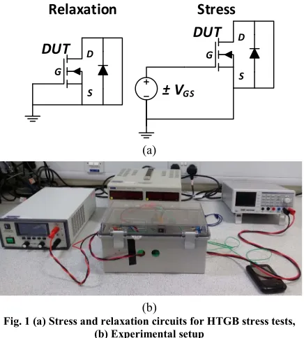
In [7] HTGB tests were performed for obtaining prediction of the lifetime of the device using the integrity of the gate oxide. The shift of the threshold voltage, which is caused by Fowler-Nordheim tunneling and is the primary mechanism related to gate oxide failures, was defined as degradation cursor. The HTGB stress tests performed in [7] were done at gate voltages higher than the recommended operating gate voltage. This approach was considered in the accelerated stress tests performed in this paper, consisting in a high voltage gate stress at high temperature and a long time relaxation at VGS=0. The long relaxation time before the characterization of the stressed device has been used in order to consider the stress on the gate oxide more permanent and not recoverable. The objective of these tests was stressing the oxide and evaluate the impact of a stressed oxide on TSEPs for SiC MOSFETs. Commercially available TO-247 packaged 650 V SiC trench MOSFETs and 650 V Si IGBTs were subjected to positive and negative HTGB stress tests at a temperature of 150 °C, which was controlled using a small DC heater attached to the device. During the stress tests the drain and source were shorted. Once the stress time finished, the gate and source terminals of the device were shorted, until the characterization of the device (output, transfer and 3rd quadrant characteristics) at ambient temperature using a
Tektronix curve tracer model 371B. The schematics of the stress
and relaxation circuits are shown in Fig. 1(a), together with the experimental setup, shown in Fig. 1(b)
Fig. 2(a) shows measured transfer characteristics for two SiC MOSFETs which were subjected to HTGB stress of 40 V and -40 V at a temperature T of 150 °C respectively The transfer characteristics were measured at ambient temperature after a relaxation time of 16 hours at VGS= 0. Fig. 2(b) shows the measured transfer characteristics for the Si IGBTs subjected to the same stress and a relaxation period of 5 hours.
In the case of the SiC trench MOSFET, as described before, BTI causes the shift of the threshold voltage of the device, with a positive stress generating a positive drift of the threshold voltage and a negative stress causing a negative drift of the threshold voltage. For the same absolute stress, observing the results in Fig. 2, the impact of BTI is higher for negative stresses. This phenomenon is not observed for the evaluated Si IGBT, as shown in Fig. 2(b).
The output characteristics after the positive and negative HTGB stresses are shown in Fig. 3 and Fig. 4 respectively. In the case of the SiC MOSFET, as shown in Fig. 3(b) and Fig. 4(b), the change in the output characteristics is evident, with an increase of the on-state resistance caused by PBTI and a reduction of the on-state resistance caused by NBTI. The impact of the threshold voltage shift caused by BTI is more apparent at low gate-source voltages, as will be discussed later on this paper. For both positive and negative stresses there is no noteworthy change of the output characteristics in the case of the Si IGBT (minor variations which can be attributed to the measurement equipment) as shown in Fig. 3(a) and Fig. 4(a).
(a)
[image:3.612.336.537.57.355.2](b)
Fig. 2 Impact of BTI on the transfer characteristics. (a) SiC MOSFETs, (b) Si IGBTs
(a)
(b)
Fig. 1 (a) Stress and relaxation circuits for HTGB stress tests, (b) Experimental setup
± V
GSDUT
G D
S
DUT
G D
S
[image:3.612.63.281.62.304.2]In the case of the SiC MOSFET, the accelerated stress tests have a clear impact on the output and transfer characteristics. The shift in the transfer and output characteristics caused by BTI will have an impact on the electrical parameters used as TSEPs, hence its use as junction temperature indicators should be assessed.
The stresses used are highly accelerated and may not be representative of real degradation during operation, however it is important to identify that in situations where there gate oxide is subjected to longer stresses than the typical gate switching operation, like power cycling or long stand-by periods with the gate biased at negative voltages, there can be a higher peak threshold voltage shift. This will have implications on junction temperature measurement using TSEPs and the reliability of the power module.
III. IMPACT OF GATE OXIDE RELIABILITY ON TSEPS FOR SIC
MOSFETS
As the results in section II shown, BTI in SiC MOSFETs has an impact on the electrical parameters, starting with the threshold voltage itself. This can be critical if these parameters are used for junction temperature estimation, as the measurements could be highly inaccurate, depending on the stress on the gate oxide and the resulting threshold voltage shift.
For the investigation presented in this paper, accelerated stress tests have been performed as the objective is characterizing the impact of the threshold voltage shift on the electrical parameters. In addition, low gate driver voltages and
high gate resistances have been used to improve the temperature sensitivity of the electrical parameters as indicated in [15, 16].
A. ON-State Resistance
The on-state resistance of a MOSFET RDS-ON is comprised of 3 main components as defined in [3, 15] and it is given by (1).
RDS-ON ~ Rch + RJFET + Rdrift (1)
where Rch is the channel resistance, RJFET the resistance of the JFET region and Rdrift the resistance of the blocking drift layer. In the case of Si MOSFETs the contribution of channel resistance is small as the dominant resistance is Rdrift. If the gate structure of the MOSFET is a trench gate, the JFET resistance is eliminated and (1) can be simplified to
RDS-ON ~ Rch + Rdrift (2)
In the case of SiC MOSFETs, the contribution of Rch to the total on-state resistance is higher [3, 15] as a thinner drift layer is required for blocking the same voltage. The channel resistance is given by (3) [3], where it can be observed that it is affected by the gate driver voltage and temperature (threshold voltage and mobility).
(3)
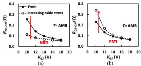
For a constant temperature, the measured on-state resistance has been characterized using a low sensing current of 50 mA (linear region of the output characteristics). The results are presented in Fig. 5, for both PBTI and NBTI.
From the results in Fig. 5 is clearly observed how PBTI increases the measured on-state resistance while NBTI reduces the measured on-state resistance. The shift of VTHcaused by BTI will be more apparent if the devices are driven with low gate voltages, as it will have a higher impact on the channel resistance. This is observed for both PBTI and NBTI.
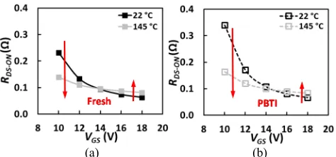
Both the channel resistance and drift resistance are affected by temperature, but they have opposed temperature coefficients [17, 18]. This causes a change of the overall temperature coefficient depending on which resistance element contributes more to the total resistance. The on-state resistance was characterized at ambient and 145 °C for both the positive and negative gate stresses and the results are shown in Fig. 6 and Fig. 7.
[image:4.612.55.295.60.179.2](a) (b)
Fig. 4 Impact of NBTI on the output characteristics. (a) Si IGBT, (b) SiC MOSFET
[image:4.612.56.293.211.340.2](a) (b)
Fig. 3 Impact of PBTI on the output characteristics. (a) Si IGBT, (b) SiC MOSFET
(a) (b)
[image:4.612.320.560.570.683.2]In the case of NBTI, the Zero Temperature Coefficient (ZTC) of the MOSFET has reduced from 14 V to 11 V, and the temperature sensitivity of RDS-ONat VGS=10 V has reduced from -0.88 mΩ/°C to -0.11 mΩ/°C. For the MOSFET subjected to positive gate stresses, BTI causes the increase of the ZTC point from 14 V to 15 V and the temperature sensitivity for a gate voltage of 10 V increases from -0.75 mΩ/°C to -1.43 mΩ/°C.
At low gate voltages, if the junction temperature is known, the on-state resistance can be used for identifying gate oxide degradation and threshold voltage shift. At high gate voltages where the contribution of the channel resistance is minimized, BTI has a lower impact on the on-state resistance, however its impact on current sharing for parallel devices [19] would require further evaluation.
B. Body diode voltage
The voltage across a PN junction during conduction is a well-established TSEP and it can be used for diodes, IGBTs and the body diode of MOSFETs [4, 20].
In the case of a PiN diode like the parasitic body diode of a MOSFET [20], at low currents, the forward voltage decreases with temperature as its temperature dependency is inversely proportional to the intrinsic carrier concentration, which increases with temperature. It is a widely used TSEP [21] for example for determining the thermal impedance during power cycling tests [20, 22, 23].
Compared to a silicon PN junction, SiC PN junctions have a higher built-in voltage due to the wide bandgap characteristics. During reverse conduction of a current, when the gate-source voltage is 0, a positive potential appears at the p-body to n-- SiC
interface and an inversion channel is formed. Part of the current
circulates through the channel, hence VSD reduces. This phenomenon is called body effect and it is explained in more detail in [20, 24]. A negative gate-source voltage closes the channel properly and the current circulates only through the body diode, hence VSDincreases to the expected value for a SiC PN junction. Fig. 8 shows the impact of the gate bias on the calibration of VSD as a function of temperature. It is clear how the voltage shifts upwards with the increasing negative bias as the body effect is minimized
In both [22, 23] the use of a negative voltage is recommended for using the body diode voltage as TSEP, in order to minimize the impact of the threshold voltage shift caused by BTI on the junction temperature measurement.
Using the test setup presented in Fig. 1, two SiC MOSFETs underwent HTGB stress tests, with a device subjected to a gate voltage stress VGS-stress of 35 V during 30 minutes at 150 °C and the other device subjected to VGS-stress= -35 V during 30 minutes at 150 °C. The stress was followed by a recovery phase of 16 hours with the gate and source terminals shorted, after which the forward voltage across the body diode was characterized as a function of temperature for a current of 50 mA. The results are presented in Fig. 9 for the negative gate stress and Fig. 10 for the positive stress. Gate-source voltages of 0 V and -4 V have been used for this characterization.
The results in Fig. 9 and Fig. 10 show that when the device is biased at VGS=0 there is a shift of the calibration curves used for determining the junction temperature: NBTI causes a downwards shift of the TSEP while PBTI causes the upwards
[image:5.612.55.292.55.172.2](a) (b)
Fig. 6 On-state resistance as a function of the gate voltage at low and high temperature (a) Fresh device (b) NBTI impact
[image:5.612.54.291.202.313.2](a) (b)
Fig. 7 On-state resistance as a function of the gate voltage at low and high temperature (a) Fresh device (b) NBTI impact
Fig. 8 Impact of the negative gate bias on VSD as function of
temperature. ISD= 50 mA
Fig. 9 Impact of NBTI on VSD as function of temperature.
[image:5.612.357.515.387.514.2] [image:5.612.353.524.553.684.2]shift. The shift is more apparent for the negative stress, with an average shift of – 306 mV caused by NBTI and an average shift of + 65 mV caused by PBTI.
In the case of PBTI biasing the device negatively clearly minimizes the impact of the threshold voltage shift on the TSEP, however this effect is not that apparent for the NBTI stresses. In this situation a lower gate voltage would be required for minimizing the body effect and compensate the negative shift of the threshold voltage. A gate voltage of -4 V is the maximum gate voltage recommended for the evaluated device, hence using a higher negative gate voltage during the temperature measurement sequence would increase the stresses on the gate oxide and it would affect the reliability of the gate oxide during the tests.
It is important to mention that these curves also indicate that if the temperature is known, the threshold voltage shift due to BTI could be detected using VSD at low currents. The authors are currently working on this topic.
C. Drain Current Switching rate
The temperature sensitivity of the switching rate of the drain current dIDS/dt of SiC MOSFETs was investigated in [16, 25]. It was shown that it increases with temperature, hence it can be used as TSEP for SiC MOSFETs. The temperature sensitivity of the switching rate of the drain current is given by (4).
(
)
− −
=
⋅ dT
dV V
t V dT d dt dV dT dt
I
d TH
TH GS
GS
DS β ( ) β
2
(4)
The change of the transfer characteristics shown in Fig. 2(a) clearly indicates that the switching transient would be affected by BTI.
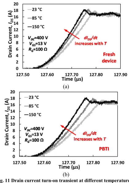
The impact of temperature on the switching rate of a SiC trench MOSFET was characterized using a traditional double pulse test setup. The turn-on transient of the SiC MOSFET using a unipolar gate driver with VGS,OFF= 0 V and VGS,ON= 13 V and a gate resistance of 100 Ω is shown in Fig. 11(a) for the fresh device and in Fig. 11(b) after being subjected to HTGB stress of 40 V at 150 °C during one hour and 16 hours relaxation with
VGS=0. The gate voltage and gate resistance values have been selected to maximize the temperature sensitivity of dIDS/dt, as described in [15, 16]. From the results shown in Fig. 11, the increase of dIDS/dt with temperature is observed for the device
subjected to PBTI, however the impact of the positive shift of
VTH is clearly perceived, with an apparent reduction of the switching rate for the same junction temperature.
In the case of the device subjected to negative HTGB stresses (-40 V at 150 °C during one hour), the threshold voltage decreases and it has also an impact on the switching rate. The measured transients for a temperature of 23 °C are shown in Fig. 12, where it is clearly observed how NBTI causes the increase of the switching rate of the drain current.
[image:6.612.333.543.55.354.2]The measured dIDS/dt, calculated as the slope of the linear regression is shown in Fig. 13 for both PBTI and NBTI. The gate voltage used was 0/13 V and the external gate resistances were 47 and 100 Ω. In these measurements the temperature was 23 °C. From the results in Fig. 13 it is observed that the impact of NBTI is higher than PBTI.
Fig. 10 Impact of PBTI on VSD as function of temperature.
ISD= 50 mA (a)
(b)
Fig. 11 Drain current turn-on transient at different temperatures (a) Fresh device (b) PBTI
[image:6.612.342.539.557.687.2]During the performed tests it was observed that it is possible to measure the same switching transient for two different temperatures. This is shown for PBTI in Fig.14 and it could have implications on determining the junction temperature using the switching rate as TSEP.
In the case of NBTI, a clear increase of the switching rate has been identified in this paper. In real application, if a negative gate voltage is used for turning off the devices during standby period at high temperature [26], a negative shift of the threshold voltage can appear, thereby causing a faster switching transient during turn-on.
D. Gate current plateau and drain voltage switching rate
In [16] the temperature sensitivity of the gate current plateau
IGP for SiC power MOSFETs was identified and it was shown that its value is dependent of the threshold voltage. Hence, the accuracy of this TSEP can also be affected by BTI.
As shown in section III.C, as temperature increases the MOSFET switches faster. At turn-on, the gate current plateau is reached when the drain current reaches the load current value and its value is given by (5) [27].
1 ∙
∙ ∙ (5)
In the case of SiC MOSFETs, the gate current plateau for a determined load current has a higher value as temperature increases [16], however from (5) it is also clearly observed how the threshold voltage shift caused by BTI would have an impact on the gate current plateau value.
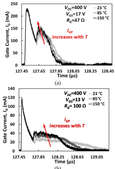
Fig. 15 shows the measured gate current transient during turn-on at different temperatures for the evaluated SiC trench MOSFET. When the device is switched at higher speed, using a gate voltage VGS=17 V and gate resistance RG =47 Ω, the temperature sensitivity is less apparent than when the device is switching at a lower switching rate, VGS=13 V and RG =100 Ω, as the results in Fig. 15(a) and Fig. 15(b) show. In addition to the more defined transient, Fig. 15(b) also shows an improved temperature sensitivity of the gate current plateau duration, more apparent at a lower switching rate.
For PBTI, the measured gate current transients at a temperature of 85 °C, using a gate voltage of 13 V and a gate resistance of 100 Ω, are shown in Fig. 16(a), where it is observed that the positive shift of VTH causes a reduction of IGP. Fig, 16(b) shows how the same transient can be measured at two different temperatures in the case of a shift of the threshold voltage caused by PBTI. The gate current transients correspond to the drain current transients shown in Fig. 11 and Fig. 14(b).
[image:7.612.60.288.56.361.2]From the results presented in Fig. 15 and Fig .16 there is an apparent sensitivity of the duration of the plateau duration when the device is driven at low switching rates. The plateau duration represents the part of the turn-on transient when the Miller capacitance is charged and the drain-source voltage VDSdrops. Fig. 17 shows the VDS transients during turn-on of the SiC trench
Fig. 13 Impact of BTI on the average dIDS/dt during turn-on of SiC
MOSFETs (a)
[image:7.612.345.535.57.335.2](b)
Fig. 15 Gate current turn-on transient of a SiC MOSFET at different temperatures. (a) VGS=17 V, RG =47 Ω (b) VGS=13 V, RG =100 Ω
MOSFET at both high and low switching rates. In both Fig. 17(a) and Fig. 17(b) the increasing dIDS/dt and lower VTH with temperature are reflected in the VDS transient. However, when the device is switched at a lower rate there is an apparent temperature sensitivity of dVDS/dt, as Fig. 17(b) shows.
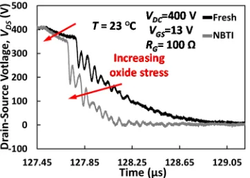
[image:8.612.81.261.55.331.2]The impact of PBTI on the VDS turn-on transient is shown in Fig 18, where it is shown that for the same temperature PBTI causes a slower VDS transient.
For NBTI, the measured VDS turn-on transients corresponding to the IDS transients in Fig. 12 (measured at ambient temperature using a gate driver voltage of 13 V and a gate resistance of 100 Ω) are shown in Fig. 19. In this case the results clearly show the impact of the lower threshold voltage due to NBTI. Together with the higher dVDS/dt, the impact of the increased dIDS/dt is also observed. The reduced VTH can also aggravate the issue of parasitic turn-on [28].
IV. CONCLUSION
In this paper the impact of the threshold voltage shift caused by BTI on the electrical parameters used for measuring the junction temperature indirectly (TSEPs) has been analyzed.
The TSEPs evaluated in this paper are the on-state resistance, the body diode voltage at low currents, the drain current, gate current and drain voltage transients during turn-on. The temperature sensitivity of the switching transients is more apparent if the devices are switched at lower rates and it has been shown that the threshold voltage shift caused by BTI will have an impact on the junction temperature measurement that can lead to inaccurate temperature measurements.
However, if the temperature of the device is known or can be identified by different means, these electrical parameters could be used for assessing the gate oxide reliability and VTH
(a)
(b)
Fig. 16 (a) Impact of PBTI on the gate current transient during turn-on, (b) Overlapping gate current transients caused by PBTI
(a)
[image:8.612.351.529.56.329.2](b)
Fig. 17 Drain-source voltage transient during turn-on at different temperatures. (a) VGS=17 V, RG =47 Ω (b) VGS=13 V, RG=100 Ω
Fig. 18 Impact of PBTI on the drain-source voltage transient during turn-on
[image:8.612.352.533.553.682.2] [image:8.612.77.261.555.685.2]shift. An example of this could be monitoring the electrical parameters off-line during stand-by periods or before starting operation.
In the case of the on-state resistance if the contribution of the channel resistance to the total on-state resistance is maximized using a lower VGS, it could be a good indicator of VTH shift. The impact of the PBTI on the body diode voltage as TSEP can be minimized if a negative gate voltage is used, hence removing the body effect and the impact of VTH on the 3rd quadrant characteristics.
Monitoring both junction temperature and VTHshifts would be fundamental for assessing the reliability of modules using SiC power MOSFETs. In this research highly accelerated stress tests were used for evaluating the impact of BTI. Further research is recommended on this topic, especially to develop tests methods for analyzing the impact of real mission profiles on the threshold voltage shift due to BTI.
REFERENCES
[1] X. She, A. Q. Huang, L. Ó, and B. Ozpineci, "Review of Silicon Carbide Power Devices and Their Applications," IEEE Transactions on Industrial Electronics, vol. 64, no. 10, pp. 8193-8205, 2017.
[2] C. Herold, M. Schaefer, F. Sauerland, T. Poller, J. Lutz, and O. Schilling, "Power cycling capability of Modules with SiC-Diodes," in CIPS 2014; 8th International Conference on Integrated Power Electronics Systems, 2014, pp. 1-6.
[3] T. Aichinger, G. Rescher, and G. Pobegen, "Threshold voltage peculiarities and bias temperature instabilities of SiC MOSFETs,"
Microelectronics Reliability, vol. 80,pp. 68-78, 2018/01/01/ 2018. [4] N. Baker, M. Liserre, L. Dupont, and Y. Avenas, "Junction temperature
measurements via thermo-sensitive electrical parameters and their application to condition monitoring and active thermal control of power converters," in Industrial Electronics Society, IECON 2013 - 39th Annual Conference of the IEEE, 2013, pp. 942-948.
[5] M. Beier-Moebius and J. Lutz, "Breakdown of Gate Oxide of SiC-MOSFETs and Si-IGBTs under High Temperature and High Gate Voltage," in PCIM Europe 2017; International Exhibition and Conference for Power Electronics, Intelligent Motion, Renewable Energy and Energy Management, 2017, pp. 1-8.
[6] Z. Chen, Y. Yao, M. Danilovic, and D. Boroyevich, "Performance evaluation of SiC power MOSFETs for high-temperature applications," in Power Electronics and Motion Control Conference (EPE/PEMC), 2012 15th International, 2012.
[7] S. A. Ikpe, J.-M. Lauenstein, G. A. Carr, D. Hunter, L. L. Ludwig, W. Wood, et al., "Silicon-Carbide Power MOSFET Performance in High Efficiency Boost Power Processing Unit for Extreme Environments,"
Additional Conferences (Device Packaging, HiTEC, HiTEN, & CICMT),
vol. 2016, no. HiTEC, pp. 000184-000189, 2016/05/01 2016.
[8] D. B. Habersat, A. J. Lelis, and R. Green, "Measurement considerations for evaluating BTI effects in SiC MOSFETs," Microelectronics Reliability, vol. 81,pp. 121-126, 2018/02/01/ 2018.
[9] A. J. Lelis, R. Green, and D. B. Habersat, "SiC MOSFET threshold-stability issues," Materials Science in Semiconductor Processing, vol. 78,pp. 32-37, 2018/05/01/ 2018.
[10] R. Green, A. J. Lelis, and D. B. Habersat, "Measurement Issues Affecting Threshold-Voltage Instability Characterization of SiC MOSFETs,"
Materials Science Forum, vol. 858,pp. 461-464, 2016.
[11] K. Puschkarsky, T. Grasser, T. Aichinger, W. Gustin, and H. Reisinger, "Understanding and modeling transient threshold voltage instabilities in SiC MOSFETs," in 2018 IEEE International Reliability Physics Symposium (IRPS), 2018, pp. 3B.5-1-3B.5-10.
[12] K. Puschkarsky, H. Reisinger, T. Aichinger, W. Gustin, and T. Grasser, "Understanding BTI in SiC MOSFETs and its impact on circuit operation," IEEE Transactions on Device and Materials Reliability, pp. 1-1, 2018.
[13] G. Ron, L. Aivars, and H. Daniel, "Threshold-voltage bias-temperature instability in commercially-available SiC MOSFETs," Japanese Journal of Applied Physics, vol. 55, no. 4S, p. 04EA03, 2016.
[14] A. J. Lelis, R. Green, D. B. Habersat, and M. El, "Basic Mechanisms of Threshold-Voltage Instability and Implications for Reliability Testing of SiC MOSFETs," IEEE Transactions on Electron Devices, vol. 62, no. 2, pp. 316-323, 2015.
[15] J. Ortiz Gonzalez and O. Alatise, "Impact of the gate driver voltage on temperature sensitive electrical parameters for condition monitoring of SiC power MOSFETs," Microelectronics Reliability, vol. 76-77,pp. 470-474, 2017/09/01/ 2017.
[16] J. O. Gonzalez, O. Alatise, J. Hu, L. Ran, and P. A. Mawby, "An Investigation of Temperature-Sensitive Electrical Parameters for SiC Power MOSFETs," IEEE Transactions on Power Electronics, vol. 32, no. 10, pp. 7954-7966, 2017.
[17] D.-L. Dang, S. Guichard, M. Urbain, and S. Raël, "Characterization and modeling of 1200V – 100A N – channel 4H-SiC MOSFET," presented at the Symposium de Genie Electrique, Grenoble, France, 2016. [18] G. Wang, J. Mookken, J. Rice, and M. Schupbach, "Dynamic and static
behavior of packaged silicon carbide MOSFETs in paralleled applications," in IEEE Applied Power Electronics Conference and Exposition - APEC 2014, 2014, pp. 1478-1483.
[19] J. Hu, O. Alatise, J. A. O. González, R. Bonyadi, L. Ran, and P. A. Mawby, "The Effect of Electrothermal Nonuniformities on Parallel Connected SiC Power Devices Under Unclamped and Clamped Inductive Switching," IEEE Transactions on Power Electronics, vol. 31, no. 6, pp. 4526-4535, 2016.
[20] J. Lutz, H. Schlangenotto, U. Scheuermann, and R. De Doncker,
Semiconductor Power Devices. Physics, Characteristics, Reliability, 2 ed.: Springer-Verlag Berlin Heidelberg, 2018.
[21] D. L. Blackburn and D. W. Berning, "Power MOSFET temperature measurements," in 1982 IEEE Power Electronics Specialists conference, 1982, pp. 400-407.
[22] F. Kato, H. Tanisawa, K. Koui, S. Sato, T. Aoki, Y. Murakami, et al., "Effect of forward voltage change depending on gate voltage in body diode of SiC-MOSFET at thermal transient testing for analysing SiC power module package," in 2017 23rd International Workshop on Thermal Investigations of ICs and Systems (THERMINIC), 2017, pp. 1-4.
[23] C. Herold, J. Sun, P. Seidel, L. Tinschert, and J. Lutz, "Power cycling methods for SiC MOSFETs," in 2017 29th International Symposium on Power Semiconductor Devices and IC's (ISPSD), 2017, pp. 367-370. [24] Dolny Sapp, Elbanhaway, and Wheatley, "The influence of body effect
and threshold voltage reduction on trench MOSFET body diode characteristics," in 2004 Proceedings of the 16th International Symposium on Power Semiconductor Devices and ICs, 2004, pp. 217-220.
[25] S. Jahdi, O. Alatise, P. Alexakis, L. Ran, and P. Mawby, "The impact of temperature and switching rate on the dynamic characteristics of silicon carbide Schottky barrier diodes and MOSFETs," IEEE Transactions on Industrial Electronics, vol. 62, no. 1, pp. 163-171, 2015.
[26] D. P. Hamilton, M. R. Jennings, A. Pérez-Tomás, S. A. O. Russell, S. A. Hindmarsh, C. A. Fisher, et al., "High-Temperature Electrical and Thermal Aging Performance and Application Considerations for SiC Power DMOSFETs," IEEE Transactions on Power Electronics, vol. 32, no. 10, pp. 7967-7979, 2017.
[27] B. J. Baliga, Fundamentals of Power Semiconductor Devices: Springer, 2008.