A junction level study of the
activation process in nanowire
networks
A thesis presented to the University of Dublin, Trinity College
for the degree of
Doctor of Philosophy in Chemistry
by
Fabio Niosi
Under the supervision of Prof. John Boland
School of Chemistry & CRANN
Trinity College Dublin
i
Declaration
I, the undersigned, declare that this work has not previously been submitted as an exercise for a degree at this, or any other University, and that unless otherwise stated is my own work. Elements of this work that have been carried out jointly with others or by collaborators have been duly acknowledged in the text.
I agree to deposit this thesis in the University’s open access institutional repository or allow the library to do so on my behalf, subject to Irish Copyright Legislation and Trinity College Library conditions of use and acknowledgement.
_______________________ ________________
ii
Summary
Over the past decade, the growth and continued improvement of electronic devices has pushed technologies beyond perceived limits. Extremely complicated devices based on single atom transistors and touch-screens made of an expensive and rare materials are examples of the limits which with the technological world are currently dealing. Alternative solutions are needed to improve and enhance our current devices. In this context, the integration of nanowires in the pre-existing devices such as FIN-FETs or GAA-FETs represents the new frontier of fabrication that aims to improve performances and scalability at the same time.
Here we study the electrical properties of single nanowires (NWs) devices and networks that comprise of them. We use Ag NWs, coated with a polyvinylpyrrolidone (PVP) passivation layer, as a platform material to study the electrical activation of nanowire networks (NWNs). Although the passivation layer is often considered as an obstacle to overcome, in this study we exploit its properties to increase the functionality of the device. The role of the junctions, or more precisely the metal insulator metal structures created between NWs, is crucial since it can facilitate the formation of a conductive filament (CF) which bridges the cores of the NWs modulating electrical conduction. Through experimental evidence and extensive simulation work, we propose a model that describes the formation of CFs within junctions thereby enabling conduction across NW films. Combining the results obtained from single wire devices and networks enables us to distinguish between two different conduction mechanisms, one based on a tunnelling effect and one related to ohmic conduction.
iii
in which networks and junctions follow the same scaling laws independent of their electrical properties (i.e. material type, coating layer, thickness of the layer). Exploiting this dynamical model we can obtain information about the activation of the system and its conductivity evolution as the current flows through it. In defining two scaling coefficients we can distinguish between the different types of activations. One, which occurs through an electrical percolating path defined as “Winner-Takes-All” paths (WTA) and one that instead evolves in a more homogenous way. Thanks to a voltage contrast technique it was possible to actually visualize the formation of the WTA path within the NWNs. Through further characterizations, we prove that by modulating the amount of current used to set the device we can access different conductance states or memory levels that have vastly different retention times. Moreover, simulations support experimental evidence that the WTA path represents the most efficient way for networks to transmit charge from one electrode to the other. Simulations also provide insights into network entropy that showed how the connectivity evolution proceeds in the network as the current is increased.
iv
Acknowledgements
I would like to thank my supervisor Prof. John J. Boland for giving me the opportunity to proceed my studies within the Trinity College Dublin. This challenging chance enable me to pursue my research carrier and improve my skills within the scientific world. I would to thank Dr. Allen T. Bellew that was a wonderful guide during the first year of my PhD introducing me to the everyday challenges behind the project and the techniques needed for the device fabrication. I am very grateful to Hugh Manning for the precious help provided to me for the fabrication and electrical tests of devices.
I would also kindly thank my colleagues Dr. Shaun Mills, Dr. Curtis O’Kelly and Dr. Jessamyn Fairfield for the help and tips useful to address my project in the right direction and Mary McCarthy and Rachel Kavanagh for their precious work within the Boland research group.
v
Contents
Declaration i
Summary ii
Acknowledgments iv
Contents v
List of figures viii
List of tables xii
List of abbreviations xiii
List of publications xvi
Chapter 1 – Introduction 1
1. Introduction 1
1.2 Memristor devices 5
1.2.1 Memory devices 9
1.2.2 ReRam devices 10
1.3 Switching mechanism 12
1.4 Conductive filament formation 15
1.5 1D materials-nanowires 20
1.5.1 Transparent Conductors 22
1.5.2 Nanowire base memory devices 26
1.5.3 Neuromorphic applications 30
1.6 Thesis outline 34
vi
Chapter 2 - Equipment and methods 41
2.1 Microscopy 41
2.1.1 SEM Scanning Electron Microscopy 42
2.1.1.1 Electron-sample interaction 44
2.1.1.2 PVC Passive Voltage contrast technique 48
2.1.2 TEM Transmission Electron Microscopy 51
2.1.3 Energy dispersive x-ray spectroscopy 52
2.2 Nanofabrication 54
2.2.1 Single and Crossed Nanowire Fabrication 56
2.2.2 Nanowire Network Fabrication 60
2.2.3 Electrode deposition 62
2.3 Nanowires 63
2.4 Electrical measurements setup 67
2.5 Conclusion 70
References 71
Chapter 3 - Activation process 73
3.1 State of the art 74
3.2 Proposed model for the activation 79
3.2.1 Junction dominate assumption (JDA) 79
3.2.2 Multi-Nodal Representation (MNR) 80
3.2.3 Capacitance model 83
3.2.4 Memristive model 83
3.3 Electrical characterization 85
3.3.1 Activation study - sourcing voltage 85
3.3.2 From macroscale to microscale 90
3.4 Further characterization 104
3.4.1 Decay time 104
3.4.2 Temperature dependence 108
Conclusion 111
vii
Chapter 4 - Self-similar scaling behaviour 115
4.1 Self similar scaling behaviour 116
4.2 Formation of WTA paths simulations 120
4.3 Experimental observation of the conductance plateaus
and WTA path 124
4.4 Visualization of WTA in NWNs 128
4.4.1 OFF and Transient regimes – Path selection 130 4.4.2 Power Law (PL) regime - WTA path 131 4.4.3 Post Power Law (PPL) regime – multiple paths 133
4.5 Energy dissipation within NWNs 134
Conclusion 139
References 140
Chapter 5 - Other network materials 143
5.1 Same scaling, different materials 144
5.1.1 Ag based materials 145
5.1.2 Cu NWNs 150
5.1.3 Ni NWNs 155
5.2 Switching properties of NWNs 157
5.2.1 Nonpolar resistive switching - AgTiO2 NWNs 158 5.2.2 Unipolar resistive switching - Cu NWNs 163 5.2.2 Unipolar resistive switching - Ni NWNs 165
5.3 Conclusion 166
References 168
viii
List of figures
1.1 Moore’s law 2
1.2 GAA mosfet Si Nw 5
1.3 Number or publication and citations about memristor 6 1.4 I-V characteristic of unipolar, bipolar and complementary
resistive switching 7
1.5 Memristor devices 8
1.6 Floating gate with schematic 9
1.7 Valence change, electrochemical and thermochemical mechanism 13
1.8 Cyclic voltammograms measurements 14
1.9 Variable gap model 16
1.10 Activation of a HfOx cell 18
1.11 Schematic of the electrochemical process 19
1.12 Resistance vs filament radius 20
1.13 Number or publication and citations about 0, 1 and 2D materials 21
1.14 Transparency vs sheet resistance 23
1.15 Processes to reduce the junction resistance 24 1.16 Number of bending vs resistance for different materials 25 1.17 NiO device with the relative I-V characteristic 27 1.18 AgTiO2 device showing uni and bipolar resistive switching 28
1.19 Formation and dissolution of CF within NW device 29
1.20 Images of a NWN and a neuronal network 31
1.21 TEM image of an Ag junction and cartoon of a neuron 32 1.22 Characterization of an AgS network through electrical pulses 34 2.1 Schematic of a scanning electron microscope (SEM) 44 2.2 Simulation of electron penetration within different materials 45
2.3 Interaction volume 46
2.4 Inelastic mean free path curve 47
ix
2.6 PVC examples 50
2.7 Internal configuration of SEM and TEM 52
2.8 EDX and interaction between x-ray and matter 53
2.9 Positive and negative photoresist 55
2.10 Work-flow for an EBL sample 56
2.11 Tarek and Cryo masks 57
2.12 Image of the robot used to spray deposit NWs 60
2.13 UV spectrum of an Ag network 61
2.14 Sketch showing the spraying process 62
2.15 SEM image, sketch and optical image of an Ag network 63 2.16 TEM images of Ag NWs and length/diameter distribution 64
2.17 TEM images of different NWs material 66
2.18 Electrical setup 1 67
2.19 Electrical setup 2 68
2. 20 Two and four point setup 69
3.1 Topography images of an Ag network 75
3.2 Conductivity evolution of Ag network and PVC image 76
3.3 LIT on Ag network to show EPPT 77
3.4 Antipercolation in Ag networks 78
3.5 JDA vs MNR 82
3.6 Network evolution high 𝐼𝑐𝑐 86
3.7 Constant voltage applied 87
3.8 FFT and power law 89
3.9 Activation and low 𝐼𝑐𝑐 sweeps 88
3.10 Current dual sweeps 91
3.11 Current steps 94
3.12 Current steps-initial stage of the activation 95 3.13 Current steps-mid stage of the activation 97 3.14 Current steps-final stage of the activation 98
3.15 Voltage spike comparison 99
x
3.17 Current step on single junction device 102
3.18 Voltage and resistance behaviour for single junction device 103
3.19 Decay time on single junction 105
3.20 Conductance decay fit 105
3.21 Decay time vs 𝐼𝑐𝑐 for single junction device 106 3.22 Decay time vs 𝐼𝑐𝑐 for network device 107
3.23 Comparison decay time network and single junction 108 3.24 Optical image before and after temperature measurements 109
3.25 Conductance vs temperature 110
3.26 Threshold voltage vs temperature 111
4.1 Γ vs 𝐼𝑐𝑐 for a junction and network 117
4.2 Scaling curve for a 200 𝜇𝑚 network 118
4.3 Simulations for different alpha and A values 120 4.4 Definition of the different regions along the activation curve 122 4.5 Simulation with the relative current map traces 123
4.6 Scaling with smaller current steps 124
4.7 Zoom of 4.6 125
4.8 Comparison within different network sizes 126
4.9 PVC image of a 20 𝜇𝑚 network 128
4.10 Image of the chamber and probes contacting the physical device 129 4.11 PVC images of the OFF and transient region 130
4.12 PVC images of the PL region 132
4.13 PVC images of the PPL region 133
4.14 Scaling curve for a 500 𝜇𝑚 network with different alpha values 134 4.15 Conductance energy and entropy simulated data 137 5.1 Γ vs 𝐼𝑐𝑐 for different network materials 144
5.2 SEM images of Ag CTAB NWs 146
5.3 SEM images of Ag CTAB NWs before and after electrical tests 147 5.4 Scaling curve obtained from a 30 𝜇𝑚 network 148 5.5 AgTiO2 single wire device and SEM image of the spray solution 149
xi
5.7 Cu scaling with network as inset 151
5.8 Ultra-sparse network SEM image 153
5.9 Scaling curve and zoom for the plateaus 154
5.10 Scaling from a Ni NWN and optical picture 155
5.11 Scaling from a Ni NWN 156
5.12 BRS associated to a 20 𝜇𝑚 AgTiO2 network 159
5.13 Coexistence of BRS and URS in AgTiO2 network 161
5.14 Unipolar reset switching in AgTiO2 network 162
5.15 Optical image of a Cu NWN 163
xii
List of tables
1.1 Lithography evolution 3
1.2 Comparison between common memory devices and reram 11
2.1 Comparison of different electron sources 43
2.2 UV Lithography process 58
2.3 EBl process 59
2.4 Transmittance vs solution sprayed 62
3.1 Resistance values for different materials 80
4.1 Slope and intercept values for different materials and devices 119
xiii
List of abbreviations
AE Active Electrode
AFM Atomic Force Microscopy
BRS Bipolar Resistive Swicthing
C-AFM Conductive Atomic Force Microscopy
CBRAM Conductive Bridge RAM
CE Counter Electrode
CF Conductive Filament
CG Control Gate
Cmos Complementary Metal Oxide Semiconducutor
CNT Carbon Nano Tubes
CRS Complementary Resistive Swicthing
CTAB Cetrimonium Bromide
DRAM Dinamic Random Access Memory
DUT Device Under Test
EBL Electron Beam Lithography
ECM Electro Chemical Mechanism
EDX Electron Diffraction X-ray
EMT Effective Medium Theory
EPPs Electrical Percolating Paths
FEG Field Emission Gun
FET Field Emission Transistor
FG Floating Gate
FTO F-doped Titanium Oxide
GAA-FET Gate All Around Transistor
HRS High Resistance State
I/O Input Output
xiv
IMFP Inelastic Mean Free Path
IPA Isopropanol
ITO Indium Titanium Oxide
JDA Junction dominated Assumption
JXN Junction
LED Light Emitter Diode
LiT Lock-in Thermography Technique
LRS Low Resistance State
MIM Metal Insulator Metal
MMA Methyl Methacrylate
MNR Multi-Nodal Representation
MNWNs Metallic Nanorire Networks
MOSFET Metal Oxide Semiconductor Fet
NP Nanoparticle
NW Nanowire
NWN Nanowire Network
PDMS Polydimethylsiloxane
PEDOT:PSS Poly(3,4-ethylenedioxythiophene) Polystyrene Sulfonate
PL Power Law
PMC Programmable Metallization Cell
PMMA Poly Methyl Methacrylate
PPL Post-Power Law
PVC Passive Voltage Constrast
PVP PolyVinylPyrrolidone
QCP Quantum Conductance Point
QD Quantum Dots
RERAM Resistive Swicthing Random Access Memory
SE Secondary Electron
SEM Scanning Electron Microscopy
SMU Source Measure Unit
xv
TC Transparent Conductors
TCM Thermo Chemical Mechanism
TEM Transmission Electron Microscopy
TG Transient Growth
URS Unipolar resistive swicthing
UV Ultra Violet
VCM Valence Change Mechanism
VLS Vapor Liquid Solid
WTA Winner-Takes-All
xvi
List of publications
Manning, Hugh G., Fabio Niosi, Claudia Gomes da Rocha, Allen T. Bellew, Colin O’Callaghan, Subhajit Biswas, Patrick F. Flowers, et al. 2018. “Emergence of Winner-Takes-All Connectivity Paths in Random Nanowire Networks.”
Nature Communications 9 (1).
O’Callaghan C, C G Rocha, F Niosi, H G Manning, J J Boland, and M S Ferreira. 2018. “Collective Capacitive and Memristive Responses in Random
1
Chapter
1
Introduction
The functioning world around us relies on knowledge and information. Languages have
been developed to communicate and spread information using particular codes. For
instance, the English language has 26 different characters used to refer to different words
and concepts. Genetic code has 4 different chemical base groups, abbreviated by the
characters A, T, C and G, that combined together to form DNA strands. A particular code,
the Boolean type 1, is made of only 2 characters “0” and ”1” and is the simplest way to
represent information. Its peculiarity lays in the fact that the information, called a bit, is
the fundamental unit by which electronic devices store information. Since 1959, when
Richard Feynman at an American Physical Society meeting held his talk “there is plenty of
space at the bottom” 2, the scientific world has sought ways to optimize the density and
quality of transferred information. The capability to store more information within a
smaller volume, the writing/reading speed of bits in memory devices or the ability to
minimize the power consumption represent some of the problems the miniaturization
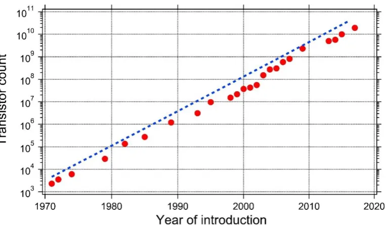
process must address. This technological evolution is summarized by Moore’s law (Fig 1.1)
2
Fig. 1.1 Moore’s law that describes the evolution of integrated circuit (IC) device densities over time 5. The blue dashed line is an eye-guide that indicated the trend doubling the
number of transistors per year.
In this law, Moore predicted that the number of transistors incorporated within a chip will approximately double every 2 years 4. The first central processing unit
(CPU) released by Intel in 1971 was capable to make simple I/O calculations. The fabrication process, back in time, was performed on a 2-inch wafer using a lithography technique 6.
Throughout the years, everyday devices such as transistors and integrated circuit allowed the development of more powerful CPUs that meet Moore’s prediction. Nowadays devices have reached unimaginable sizes yielding device densities and capabilities comparable with the dimensions of single atoms. Considering, for example, the number of operations that a single CPU can do within a second. The 4004 model (1971) was capable of 92,000 instructions per second. After five decades, the latest version of supercomputers can manage almost 1 𝑒𝑥𝑎 (1018)
instructions per second 7. Closer inspection of Fig. 1.1, however reveals a
3
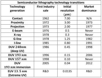
[image:21.595.124.472.163.429.2]lithography. Table 1.1 summarizes the evolution that lithography had between the 70’s and 80’s with the relative resolution 8.
Table 1.1 Lithography evolution 8 with relative resolution achievable.
Semiconductor lithography technology transitions Technology generation First industry sale Initial resolution (𝝁𝒎) Market dominance
Contact 1962 7.00 N/A
Proximity 1972 3.00 1973
Projection 1973 2.00 1977
E-beam 1976 0.5 Never
X-ray 1978 0.3 Never
G-line 1978 1.25 1982
I-line 1985 0.80 1991
DUV 𝟐𝟒𝟖𝒏𝒎 (deep UV)
1986 0.45 1998
DUV 𝟏𝟗𝟑 𝒏𝒎 1996 0.15 2006
DUV 𝟏𝟓𝟕 𝒏𝒎 1998 0.10 Never
DUV
1𝟗𝟑 𝒏𝒎 immersion
2005 0.04 2012
EUV 𝟏𝟑. 𝟓 𝒏𝒎
(Extreme UV)
R&D 0.0135 R&D
For decades, research and development went side by side as can be seen from the table 1.1 but nowadays the semiconducting industry is facing the fact that lithography is reaching its limit to top the finite feature size. The latest generation of integrated circuit (IC) are now comparable with the dimensions of a few atoms. According to the semiconductor roadmap 9, the dimension of a single transistor in
2019 will be around 5 − 10 𝑛𝑚 corresponding roughly to 20 − 40 atoms. This will inevitably cause problems such as reproducibility of the devices, leakage, increased production costs and increasingly sophisticated manufacturing technologies. There will be difficulties arising from the interaction and manipulation of single atoms to create devices. Devices such as FIN Field-Effect Transistor (Fin-FET) and multi-gate FET 10 aim to minimize these problems but yet,
[image:21.595.123.472.163.428.2]4
that can allow the continuation of Moore’s law is the memristor and its integration within the pre-existing device technologies 11. To further enhance the capabilities
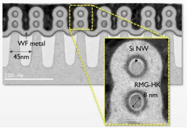
of the next generation electronic devices, the integration of 3D features is now being considered. More complex structures such as Gate–All-Around (GAA-FET) or Multi-Gate nanowires (NWs) FET are being employed to improve the properties of transistors and IC using nanostructures. Fig. 1.2 shows a practical example in which a Si nanowire is used within a GAA MOSFET device to connect source and drain electrodes 12. The Si nanowire, encapsulated within a Ge cover layer, plays a
key role within the scaling process. It enables the integration of nanometre size objects bypassing the UV lithography step and its limitation along with it. The bottom-up approach used to create the GAA device grants the possibility to create structures with sub-10 nm features, something unachievable with conventional lithography techniques. The sharp interface between the Si NW and the Ge layer also improves the electrical performances as reported by a research group on IMEC technologies 12.
The memristor, as first introduced by Chua 13, is a two terminal device capable of
5
Fig. 1.2 GAA MOSFET device, one of the first semiconducting devices with a Si NW integrated into it 12. The “Gate All Around” structure is clearly visible in the inset in which
the Si NWs are embedded in the surrounding Ge layer.
For these reasons, it is worth considering the implementation of nanowires and memristor components as a completely new paradigm for device operation. Here, following, a comprehensive introduction on memristor and Resistive Random-Access-Memory ReRAM capabilities we describe how nanowire networks (NWNs) may represent the new paradigm needed to maintain Moore’s law level performance.
1.2 Memristor devices
The term memristor, was introduced by Chua in 1971 13. According to his
pioneering work, a memristor is a nonlinear two terminal circuit element in which the resistance depends on the charge 𝑞 flowing through the device 14,15. A
[image:23.595.113.485.81.336.2]6
contacts were established to different insulating oxide layers such as 𝑁𝑖𝑂𝑥, 𝑆𝑖𝑂𝑥, 𝑇𝑖𝑂2, and 𝐴𝑙2𝑂3. The interest in Chua’s work has grown rapidly since HP reported a memristor effect 17 in a confined 𝑇𝑖𝑂
2 Metal-Insulator-Metal
(MIM) nanodevice. The interest in memristor devices, as shown in Fig.1.3, has grown abruptly in the last years thanks to their potential in electronic applications.
Fig. 1.3 Number of publications (in red) and citations (in blue) referring to memristor devices. Data acquired from https://www.scopus.com using as keyword “Memristor
device”.
Memristor devices can have different operational modes depending on the structure and the characteristic of the insulating layer used 18. In order to describe
7
Fig. 1.4 Typical I-V curves for unipolar (a), bipolar (b) and complementary resistive switching (c) devices 20,21. In unipolar devices set and reset operations are obtained
applying one voltage polarity while in the bipolar configuration to two different voltage
polarities are required to set/reset the cell. In the latter case, the complementary resistive
switching, both the mechanism described for uni/bipolar devices are present.
In a unipolar device, the two operations, SET and RESET, can be executed using the same voltage polarity as shown in Fig. 1.4 (a). The system starts at its pristine HRS and a voltage in the positive direction is used to SET the device. A current compliance 𝐼𝑐𝑐 is initially set to prevent electrical failure of the sample during the SET operation. Once the sample is in the LRS, the second positive sweep is applied without any compliance causing the RESET of the device due to the high current flowing within the device 20.
[image:25.595.107.494.79.349.2]8
The complementary resistive switching (CRS) is a more complex process and, as suggested by Linn et al 20, can be built using two bipolar resistive switches in a
[image:26.595.107.491.275.480.2]back-to-back manner. Due to this particular configuration, CRS is widely used within crossbar arrays to eliminate the leakage currents through the adjacent bars that otherwise degrades very easily the qualities of the devices. The reading operation for CRS requires higher voltages (few V) compared to URS and BRS (hundreds mV) eliminating the problem that sufficiently low voltages often cause leakage currents.
Fig. 1.5 Overview on memristor phenomena based on the different mechanisms 9. Despite
the vastness of this research field across this PhD project we will describe the
characteristics of the devices based on redox reactions with particular attention to the
redox effect materials.
9
1.2.1 Memory devices
Memory devices appear in a wide range of modern electronic devices including smartphones, TV screens, personal computers, etc. Memory is classified as volatile or non-volatile. As suggested by the name, volatile memory devices are capable of storing information as long as voltage is supplied. Shutting off the power will cause the loss of any saved data. Dynamic Ram (DRAM) and Static RAM (SRAM) are two of the most common examples of volatile memory on the market. The working principle of DRAM’s is quite simple. The charge stored on a capacitor acts as switch between the OFF state or “0” and the ON state (“1”). A transistor is coupled to the capacitor allowing the READ operation without perturbing the state itself. The combination of the capacitor as a storage unit and transistor as the reading counterpart is known as a 1C-1T technology and is capable of recording a single bit of information. This simple unit 1C-1T is then embedded within arrays to create the memory device.
Fig. 1.6 A floating gate memory device (a) and its schematic (b), readapted from 22.
10
used as long-term storage of information, most common devices are hard disk drives, read-only–memory and flash memory. The latter is now the dominant type and is used in almost all electronic equipment. Fig. 1.6 (a) schematizes the structure of the device that resembles common MOSFET 22. A floating gate (FG)
electrically isolated from the rest of the device, is positioned between the control gate and the source-drain channel and basically acts as a switch. The charges accumulating on the FG cause a screening effect affecting the control gate (CG) leading to the logic states “0” and “1”. State “1” can be obtained removing the charges from the FG by the application of a voltage or UV light. The logic states are governed by the current that flow between the source and drain; if the channel is conducting, it means that the FG is not charged resulting in the logic state “1”. Otherwise, a “0” is obtained when the current cannot flow within the device. 22,23.
Therefore, flash memories are arranged in arrays and matrix to create components within electronic devices.
In the next section the two memory devices introduced, DRAM’s (volatile) and flash (nonvolatile), will be used to make a comparison in terms of performances, endurance, and longevity with ReRAM that represents next generation of nonvolatile memories.
1.2.2 RERAM devices
11
Table 1.2 Performances comparison between conventional memory devices and ReRams
22. The 𝐹 parameter used in the table is related to the current resolution of the UV
lithography technique used.
DRAM Flash ReRAM
Cell size ≈8F2 5.44F2 4.28F2
Endurance >1015 >105 >108
Retention time >64ms 1-3 years >10years
Volatility y n Y
Resistance ratio - 5 10-1000
Read voltage - 0.6V 0.3-0.7V
Multilevel storage n y y
Energy per bit(J/bit) 4x10-15 4x10-16 >10-12
Writing speed <10ns 200μs 100ps
For decades the scalability of devices was linked to the technique resolution used for fabrication but as introduced earlier, this is no longer the case. As reported in Table 1.1, UV Lithography has reached its physical limitation (see Chapter 2), therefore, a new way of device fabrication is required. DRAM and flash memories have a limited resolution of 15 𝑛𝑚 while ReRAM exhibits higher scalability. Switching between the ON-OFF states has already been demonstrated in 10 𝑛𝑚 𝑥 10 𝑛𝑚 devices 24. Further increases in resolution are achievable since
the conduction mechanism within ReRAM is driven by ions within the insulating layer of MIM cells. Thanks to this, devices could in principle be much smaller than
10 𝑛𝑚25. The stackability of this kind of cells provides a way to re-think devices in
a 3D fashion allowing the integration of multiple MIM structures. Besides that, the power consumption and reading/writing process will be substantially improved due to the more highly confined structures. The reduction in space allows for decreased read/write voltages, reducing the total power consumption 26.
12
temperature, generated by Joule heating, (current density equal to
105𝐴 𝑐𝑚⁄ 2has been demonstrated for a 10 𝑛𝑚 𝑥 10 𝑛𝑚 device) help the carriers to diffuse faster within the insulating layer. Parameters such as endurance and retention time are on the other hand extremely dependent on the type of ReRAM used. The endurance, expressed as the number of cycles that a device can handle, can vary over a large window, almost six orders of magnitude (106 - 1012
for TaOx devices)1,22,27,28, depending on the composition of the insulating stack
material. Retention time, on the other side, is the capability to store and preserve the information over time. In order to simulate the real conditions within hard drives the retention time is often calculated under thermal stress. In a conventional flash device, retention time is estimated to be between 1-3 years. For ReRAM, independent of the material used for devices, the information can be stored for longer periods 29. This is possible thanks to the high resistance ratio,
defined as 𝑅𝐻𝑅𝑆⁄𝑅𝐿𝑅𝑆, associated to ReRAMs. Table 1.2 highlights the poor resistance ratio of flash memories in comparison to ReRAMs. Generally, higher resistance windows allows greater accuracy during the reading operation thanks to a wider operating margin.
1.3 Switching mechanism
13
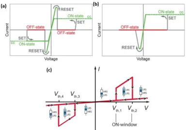
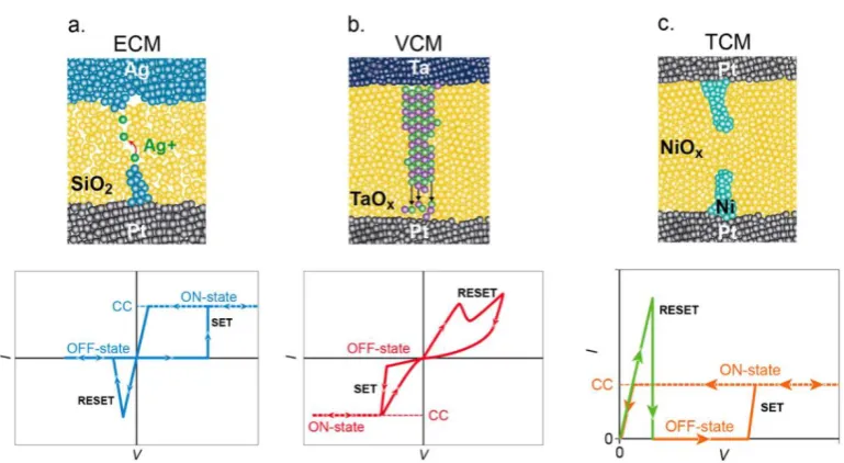
Electro Chemical Mechanism (ECM)
The ECM effect is also a bipolar effect and it is known in the literature as Conductive Bridge RAM (CBRAM) or programmable metallization cell (PMC) 30. As
the name might suggest, a redox reaction happens at the active electrode (AE) resulting in the formation of a conductive filament within the device 30 as shown
in Fig. 1.7 (a).
Fig. 1.7 Different mechanisms for the creation of a conductive filament within MIM devices captured in I-V curves 31.
The choice of the electrode material in the case of ECM is crucial; materials with high mobility such Ag, Cu or Au are commonly used as the active electrode. Their high electrochemical activity facilitates the reactions and therefore the creation of the CF. On the other side, inert materials such as W, Pt, and Ni are used as the counter electrode (CE). The role of the CE is to catalyse or to inhibit the redox reaction and therefore the CF formation. Cells performances are also heavily influenced by the AE/CE coupling in terms of energy requirements for the reactions (see Fig. 1.8). The easiest way to investigate this phenomenon is to perform cyclic voltammetry over cells made of different materials. As suggested by Tsuruoka et al 32, cyclic voltammetry measurements help to identify and prove
[image:31.595.106.491.251.462.2]14
are tested applying low voltages to prevent the switching between the ON and OFF states. On the left hand side, the curves for cells made with Cu as AE, SiO2 as
the insulating layer and different CEs32are shown. In Fig. 1.8 (b), the same type
of investigation is performed over a Cu/Ta2O5/Pt cell 32 and shows the different
electrochemical reactions happening within the device.
Fig. 1.8 Cyclic voltammograms measurements performed on different MIM devices. The voltage applied is deliberately chosen to prevent the switch within the cells 31,33. In (a) the
AE is always Cu while the CE is changed in order to test the importance of the CE material.
A different active layer is instead used in (b). A Cu/Ta2O5/Pt cell is used to highlight the
redox peaks. A comparison in terms of current within cells (two black curves in a-b) shows
the role that the active layer plays within cells.
A typical voltammetry measurement is reported in Fig. 1.8. This electroanalytical method is commonly used to understand which redox reactions take place within MIM devices formed by different materials. A subthreshold voltage is swept in both polarities and, as can be seen from Fig. 1.8, several redox peaks are observed in the voltammograms plots for different AE/CE combinations.
Valence Change Mechanism (VCM)
15
the overall resistance of the cell 34. Different reports point out that even interstitial
cations acting as mobile donors might be responsible for this conduction mechanism too. The motion of ions will induce a change in stoichiometry causing redox reactions 21. Bipolar memory behaviour is typical of VCM devices and can be
seen in Fig. 1.7 (b). Many reports correlate the switching effect to electrical pulses applied to the cell where the polarity of the voltage applied induces reduction or oxidation.
Thermo Chemical Mechanism (TCM)
This mechanism is slightly different from the first two. The main difference lies in the unipolar behaviour that this kind of devices shows. From Fig. 1.7 (c) it is possible to note how TCM can be switched between ON and OFF states using the same voltage polarity 35. The operation to set the device usually involves the use
of a current compliance 𝐼𝑐𝑐 to limit the maximum current flowing within the device
to prevent electrical breakdowns. Furthermore, the heat generated by Joule effect induces redox reactions that change the stoichiometry of the cell allowing the formation of a CF. Reset operations are instead obtained by removing 𝐼𝑐𝑐. The high current (mA range) that flows within cell can produce temperature gradients that eventually disrupt the CF growth and return the cell back to the OFF state. Due to its working principle,TCMis also known as fuse-antifuse memory. Because of the high currents and energies required for switching, TCM R&D decreased significantly in the past 5 years.
1.4 Conductive filament formation
16
approaches. Designed tests were performed over a wide variety of MIM cells to confirm that the switching mechanism is governed by the same CF growth process.
Fig. 1.9 Resistance vs diameter of a CF simulated with the variable diameter model 38 in
(a). The resistivity used for the simulations are respectively 400𝜇Ω 𝑐𝑚 for a Hf filament in red and 200 𝜇Ω 𝑐𝑚 for Cu in blue 39. In (b) the variation of the resistance as the gap
decreases.
Fig. 1.9 shows the results obtained from two different simulation models used to describe the formation process of a CF. In the first model, the resistance is calculated considering the formation of a CF, with a variable diameter, that connects the electrodes. In the second scenario, the filament initially does not connect the electrodes and therefore tunnelling effect is considered responsible for the conduction within cells. Note that due to the wide variety of materials and CF growth mechanisms, particular devices might be described by a combination of the two models 38.
Two models were introduced initially to describe bipolar switching within MIM cells. Variable diameter model is based on the migration of localized defects which, under a certain bias, leads to the formation of a CF 38. An inverse potential
will reverse the process causing the dissolution of the filament, resetting the device. The process can be simply described using an Arrhenius-type approach as:
𝑑𝜙
𝑑𝑡 = 𝐴 𝑒𝑥𝑝 (− 𝐸𝐴
17
where 𝑑𝜙 𝑑𝑡 ⁄ represents the variation of the CF diameter, 𝐸𝐴 is the activation energy for defect migration, 𝐴 is a pre-exponential constant while 𝐾𝐵 and 𝑇 are respectively the Boltzmann constant and the local temperature.
Considering then Poole-Frenkel transport mechanism, as suggested by 37,40, the
activation energy can be rewritten as a function of the applied voltage as
𝐸𝐴 = 𝐸𝐴0− 𝛼𝑒𝑉 Eq. (1.2)
Where 𝐸𝐴0is the energy barrier without voltage applied, 𝛼 is a constant related to
the hopping coefficient and V is the voltage across the device. In this picture, the diameter and consequently the CF growth will be only dependent on the bias applied to the ReRAM cell, indicating a voltage-driven process.
Fig. 1.10 depicts the CF evolution during a voltage dual sweep (0𝑉 1𝑉− 1𝑉 0𝑉) performed on a 20 𝑛𝑚 thick HFOx cell that shows bipolar (setting a 𝐼𝑐𝑐)
and complementary switching behaviour 38. A positive voltage is applied initially
18
Fig. 1.10 I-V sweeps performed on HfOx cell showing the formation of the conductive
filament 38. At the start the cell is in its virgin state and is activated through a voltage
sweep as shown in (a) reaching the current compliance 𝐼𝑐 = 1 𝑚𝐴. The following
evolution of the cell is shown in (b) with a relative cartoon of each configuration describing
the state of the device in (c).
In the variable-gap model 41, the conduction can be virtually divided in two
[image:36.595.158.440.78.319.2]19
Fig. 1.11 Schematic of the equivalent circuit for the switching process (a). In (b) a sketch that describes electrochemical processes occurring during the SET operation 41.
Fig. 1.11 (b) depicts all the mechanisms responsible for the growth of a CF 41. A
20
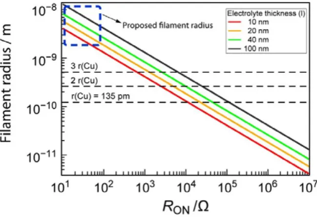
Fig. 1.12 Simulation that relates the 𝑅𝑂𝑁 (Ω) to the radius of the conductive filament
growing within the cell as the thickness changes 42. The horizontal lines represent the
diameter of filaments ending with one two or three atoms that intercepting the curves
give the 𝑅𝑂𝑁 values.
1.5 1D materials-nanowires
[image:38.595.135.460.82.304.2]21
Fig. 1.13 Literature review that describes the number of publications of different nanoscale materials over the time. Data acquired from www.scopus.com using as
keyword respectively 0D, 1D and 2D materials.
Fig. 1.13 summarizes the number of publications related to nanomaterials of distinct dimensionality 43. 0𝐷 materials, in particular quantum dots (QDs) and
nanoparticles (NPs), attract more interest thanks to their incredible surface area and catalytic properties 44. Surface area is commonly described as the ratio
between the atoms laying on the surface of a certain material respect to the bulk ones. The kinetics of reactions is deeply influenced by surface area because a bigger surface area also means that more atoms can undergo the reaction process. For this reason, nanoparticles and quantum dots are extensively studied nowadays in medicine, environmental applications, electronics, LEDs, batteries 45,46.
Recently, there has been a growing interest in 2𝐷 materials. Graphene is perhaps the most famous example with countless applications 47,48. Made of a single sheet
[image:39.595.108.487.78.293.2]22
confinement effects provide new electronic properties to 1𝐷 structures opening a window on new conduction mechanism such as tunnelling and ballistic transport
49. Mechanical properties of nanotubes and nanofibers have been widely studied
because of tensile strength of these materials 50. Scientists have recently produced
peptides nanotubes with a Young’s modulus of 19 𝐺𝑃𝑎 that could be potentially even bio-compatible 50. Core-shell and tubular nanowires have been studied for
their thermoelectric efficiency 51,52. Carbon nanotubes, thanks to their unique
crystal structures, present remarkable electrical and mechanical qualities 53,54.
Catalysis and sensors are the major applications for the metal oxide and semiconductor 1𝐷 materials 55. Yet another possibility is to assemble 1𝐷
nanomaterials into random oriented nanowire networks. This provide a natural transition between 1𝐷 and 2𝐷 materials since networks still present properties of
1𝐷 material but are incorporated into films with 2𝐷 characteristics. Therefore, the goal of this work is to study the electrical properties of metallic nanowire networks. The following sections describes the current state of the art of 1D nanomaterials with particular attention to their integration as networks within devices.
1.5.1 Transparent Conductors
Metallic nanowire networks (MNWNs) are often mentioned along with transparent conductors (TCs). Thanks to their excellent electrical and optical properties, they appear as ideal candidates for the next generation of touch screens, touch pads, and ultra-thin screens. State of the art touch screen technologies are built using layers of Indium Tin Oxide (ITO) or Fluorine-doped Tin Oxide (FTO) 56. As a result, the price of raw indium material has rapidly increased
in the last few decades 56. Doped binary compounds such Aluminium Zinc Oxide
23
devices and according to the market standards, the transparency should be higher than 90%. On the other hand, sheet resistance is crucial in lowering the energy requirement of the devices. Sheet resistance is expressed as Ω □⁄ and represents the resistance associated with a 2𝐷 layer or thin film of the material. Even in this case, according to the standards, ideal materials should have sheet resistance lower then 100 Ω □⁄ . In Fig. 1.14, the transmittance is plotted against the sheet resistance for TCs fabricated using different nanomaterial. Focusing the attention on Fig. 1.14, currently researcher goal is to obtain films with transparency over
[image:41.595.117.478.346.627.2]90 % with a sheet resistance lower then 100 Ω □⁄ . In doing this, the performances of the actual devices will be hugely boosted granting high brightness and a low power dissipation.
Fig. 1.14 Transparency vs Sheet resistance for different nanomaterials 57,58. ITO films are
currently used in devices but the properties of Ag NW networks are starting to be similar
to the ITO films. A parameter that influences the outcome, especially in terms of 𝑅𝑆, is the aspect ratio expressed as 𝑙𝑒𝑛𝑔𝑡ℎ 𝑑𝑖𝑎𝑚𝑒𝑡𝑒𝑟⁄ of the NWs. Remarkably the Ag NW network with an aspect ratio equal to 360 (black squares) has a resistance that almost
24
As can be seen, carbon based materials such as graphene or synthetic materials are not adequate due to their high resistances. The contact point resistance between nanotubes or flakes ranges from 50 𝑘Ω to 100 𝑘Ωas reported by 59. The
implementations of carbon based materials are therefore limited since homogenous films can present resistance in the order of magnitude of Gigaohms. On the other hand, metallic nanowire networks might be suitable for the purpose. As depicted by Fig. 1.14, the properties of Ag random oriented networks are close enough to match the standards of ITO films currently used as commercial devices. Ag nanowires are particularly attractive due to their low resistivity compared to Cu nanowires. Furthermore, another factor that needs to be considered is the aspect ratio of the NWs used that plays a massive role in the properties of the final device. Moreover, as will be further discussed in section 3.2.1, the quality of the films are hugely influenced by the contact point resistance or junction formed between two touching nanowires 60. For this reason, numerous reports are
focused at reducing the sheet resistance by minimizing the junction resistances. Thermal annealing 61, mechanical pressing 62, chemical etching 63 and laser welding 64,65 are examples, shown in Fig. 1.15, of techniques used to improve the quality
of the devices in order to meet industry performance standards.
Fig. 1.15 Two different approaches are mainly used to reduce the junction resistance of NWs. The first is about physical treatment such as annealing or pressing of the films or
25
With the constant market demand for flexible touch screens, another remarkable quality of MNWs is their mechanical properties. Thanks to the fact that nanomaterials can be dispersed practically within any solvent, they can be deposited very easily over any kind of surface including flexible ones 67,68, and the
[image:43.595.148.451.211.464.2]natural elasticity of the nanowire opens up the possibility of flexible devices.
Fig. 1.16 Change in resistance of different materials, used as TCs, after several bending cycles 67,69. In red the resistance ratio associated to an ITO film that degrades very quickly
as the sample is bent. The FTO film shows instead a more smoothen degradation in
comparison with ITO. The elasticity of the Ag NWNs is confirmed with an unchanged
resistance after several bending cycles.
Studies on the mechanical properties with networks sprayed over flexible substrates have revealed incredible stretching abilities. Ag NW networks deposited over on Polydimethylsiloxane (PDMS) substrates can handle repeated bending cycles without any degradation in resistance 67,69. The comparison
between ITO, FTO and Ag NWNs shown in Fig. 1.16 demonstrates how the resistance for metallic nanowires does not change after mechanical stress 67,69.
26
slow degradation of the film after several bending cycles (FTO) or an abrupt rupture after few cycles (ITO). This indicates that ITO and FTO are not suitable for realizing flexible devices. The remarkable characteristics of metallic nanowire networks, mechanical flexibility, high transparency and low sheet resistances, make them ideal candidates for transparent conductor applications. When combined with the ease of processing and scalability, MNWNs can play an important role into the new market of flexible devices.
1.5.2 Nanowire based memory devices
Several reports have highlighted the possibility to use nanowire-based devices for memory applications 70–72. These studies cover a wide range of materials including
oxide nanomaterials, core-shell structure and metallic nanowires. One of the first reports pointing in this direction was published by Kim et al in 2008 73. In their
27
Fig. 1.17 SEM image of NiO nanowire contacted by EBL (a). In (b) the I-V’s show the unipolar resistive switching between high and low resistance state 74.
In order to explain the switching between the two states, the variable diameter model was used. Due to the applied voltage, a CF grows within the oxide layer bridging the core of the NW enabling the LRS conduction. The reset operation occurs when enough heat is generated by the current to break the CF switching to the HRS. Following this publication, many other reports have demonstrated the possibility to use nanowires coated with oxide layers as active layer 75 or even
metallic nanowires 76. A fascinating alternative approach for memory device is
represented by core-shell (CS) nanowires. Thanks to their structures they can combine the excellent conductivity of metallic nanowires with the switching properties of oxide materials. In a recent report 77, Manning et al. demonstrated a
28
Fig. 1.18 In (a) TEM image of a AgTiO2 nanowire with the EDX signal that shows the
distribution of Ag and TiO2 Kα signal along the nanowire. A SEM image shows the NW
device contacted by Ag electrodes. In (b) I-V’s that show non-polar resistive switching.
Unipolar and bipolar switching can be obtained changing the 𝐼𝑐𝑐during the set operation 77.
A full characterization of the sample can be found in Fig. 1.18 (a) 77. The
Transmission Electron Microscope (TEM) image shows the structure of the CS nanowire and highlights the sharp interface between the two different materials. The chemical analysis is performed through an Electron Diffraction X-ray (EDX) characterization and shows the peaks associated with the Ag and the TiO2 along
the perpendicular dashed line. The second image in Fig. 1.18 (a) shows instead the electrical device contacted through an Electron Beam Lithography (EBL) step with Ag electrodes. In Fig. 1.18 (b) representative I-V curves demonstrate the non-polar behaviour. In fact it is possible to note how the device shows, according to different SET operations, unipolar or bipolar switching properties. The transition between HRS and LRS is explained with an approach similar to the variable-gap model introduced in the section 1.3. The TiO2 shell is considered as the active layer
in which Ag ions can diffuse and form a CF as shown in Fig. 1.19 (a-d). Depending on the voltage polarity, two CFs can be grown within the two interfaces formed by the Ag electrodes and the TiO2 layers. The non-polarity of the device can be also
29
of a weak filament within the interfaces. In this state the device, due to the poor strengthening effect of the current, cannot retain the information. Further increase of the 𝐼𝑐𝑐will bring the device within an intermediate region where the sample acts as a bipolar switch. The compliance used for the set operation is sufficient to create a CF that bridges the electrodes with the internal core of the NW setting the device in the LRS. However, the CF is not sufficiently stable within the active layer as demonstrated from the poor retention time (< 10 𝑠). A negative voltage is then sufficient to switch the device back into the HRS granting the bipolar characteristic behaviour. Lastly, for very high compliances (< 150 𝜇𝐴), the created filament can be associated to a permanent condition in which the system presents a unipolar behaviour. In this state, the device can switch to the HRS thanks to Joule heating effect taking place in voltage sweeps without compliance. The extremely high retention time, bigger than 107 𝑠, also proves the stability of the state achievable within the unipolar regime.
Fig. 1.19 Formation and dissolution of the CF within bipolar (a-b) and unipolar (c-d) regime. In order to test its endurance, the device was switched between the HRS and LRS
over different cycles (e). In (f) the conductance is plotted versus the current compliance
used for the set operation. Three different operational modes are reported. The retention
30
In terms of integration within memory devices, core-shell nanowires present several remarkable qualities. The main advantage is the richness of states accessible with one single device. Merely changing the current compliance during the set operation three different conduction mechanisms can be obtained: (i) volatile devices for currents below 10 𝑛𝐴, (ii) bipolar behaviour for currents that range between 10 𝑛𝐴 and 100 𝜇𝐴 and (iii) for currents < 150 𝜇𝐴, unipolar characteristics. Write/read voltages are usually quite low, well below 1 𝑉, helping to reduce the energy per bit required to store information. The resistance ratio is another important parameter to consider in memory devices and, as shown in Fig. 1.18 (e), depending on the compliance, different ratios can be obtained. Remarkably a ratio of 𝑅𝑟𝑎𝑡𝑖𝑜 = 104 can be achieved using the device as a bipolar
switch or 𝑅𝑟𝑎𝑡𝑖𝑜 = 105 in the unipolar regime.
1.5.3 Neuromorphic applications
Another promising application, perhaps the most fascinating one, consists of realizing artificial synaptic devices with the goal to mimic human brain behavior. The Blue Brain project 78, SpiNNaker program 79 or the True North chip 80 from IBM
are only a few examples of projects initiated to develop a platform capable of processing information as the brain does. Cross-bars arrays of memory units, mostly SDRAM, are conventionally used as skeleton networks to replicate simple
𝐼/𝑂 operations. With this approach, very dense structures with 53 × 1010neurons and 1.37 × 10¹⁴ synapses 79,80, can be achieved. In terms of
numbers, a human brain has roughly 100 billion of neurons connected through 1000 trillion of synapses. But despite the numbers reached so far with CMOS structures, the main limitation arises from the fact that these architectures often require thousands or even megawatts of energy to process information 80. It is
31
high 2𝐷 scalability, multilevel resistances, high switching speed and low power consumption are examples of the improvements that memristor bring towards the ultimate goal of brain-like or neuromorphic computation 81.
One of the first reports exploring the potentiality of nanowire networks as neuromorphic devices was introduced by Gimzewski et al in 2012 82. The
importance of this publication arises from the fact that the authors aim at mimicking the brain functionality using different approaches. Instead of focusing the attention on conventional crossbar structures, a completely new platform, based on NWNs, is used for the purpose. It is possible to note that the two systems, networks and brains, share a large number of similarities. Starting from their structures resemblance, Fig. 1.20 shows a culture of hippocampal neurons 83
and an Ag NW network treated with AgNO384.
Fig. 1.20 Similarities between NWNs shown in (a) scale bar 10 𝜇𝑚 and neuronal networks in (b) with a 50 𝜇𝑚 scale bar 83,84.
32
Dendrites are thin structures that arise from the cell body, often extending for hundreds of micrometers and branching multiple times, giving rise to complex structures called "dendritic trees". An axon is a cellular extension, enclosed within myelin sheaths, that enables the travelling of information. The interface between the axon and the dendrites is known as synapses and represents the key component for the transmission of the signal among neurons. Each synapse within the brain has a certain voltage threshold that acts as a barrier beyond which the information can be “fired”.
Fig. 1.21 A TEM image of an Ag NWs junction 85 (a) and a sketch of a neuron in (b) 86,87. In
making a paragon, the NWs junctions explicates the neuron functionalities while the
actual wires represent the connections that within the brain are made by the axons.
33
Unipolar, bipolar, complementary switches or even rectifying behavior are achievable with memdevices which not only opens up the possibility to mimic synaptic behavior but to implement additional features or functionalities 34,84. For
example, if the voltage applied to the cell is sufficient to switch to the LRS, the electrical signal can travel through the core of the wire and reach the next junction just as in neurons.
Another important characteristic of the brain is the plasticity associated with the learning mechanism. According to the theory introduced by Hebb 88,89, during the
learning process the information is stored within the brain thanks to the strengthening mechanism of neurons. Each neuron has a determinate barrier or weight associated to it. It has been proved that, during the learning process, the barriers of the neurons carrying the information is lowered 87. At the same time,
the barrier of the neurons not involved in the process will increase further helping the learning process. In the same way junctions within networks can replicate this behavior as shown in Fig. 1.22 for the case of an Ag NW network chemically treated. A triangular shape voltage sweeps (0 − 5 𝑉) is applied to the network and the current response is shown in (b) 82. A schematic representation of the
34
Fig 1.22 SEM images at different magnification of SiO2 sample containing the Pt electrodes
(a) before growing the AgNO3 network 82. In (b) the electrical signal collected from the
network that shows the current evolution as the voltage is supplied to the network. In (c)
a schematic representation describing the connectivity evolution within the film.
1.6 Thesis outline
35
36
References
1. Siemon, A. et al. Realization of Boolean Logic Functionality Using Redox-Based Memristive Devices. (2015).
2. Feynman, R. P. There’s Plenty of Room at the Bottom An Invitation to Enter a New Field
of Physics, (1959).
3. Collaert, N. Extending Moore ’ S Law : Nanowires To the Rescue, (2013).
4. Moore, G. E. Lithography and the future of Moore’s Law (2006).
5. Technological Progress - Our World in Data.
6. Intel innovation from the start, (2003)
7. Kothe, D. B. Science Prospects and Benefits with Exascale Computing, (2007). 8. R. Kapoor, R. Adner. The lithography ecosystem (2007)
9. ITRS. International Technology Roadmap for Semiconductors, (2015).
10. Nagy, D. et al. FinFET versus gate-all-around nanowire FET: Performance, scaling, and variability, (2018).
11. Cavin, R. K., Lugli, P. & Zhirnov, V. V. Science and Engineering Beyond Moore’s Law,
(2012).
12. Nws, S. et al. Imec demonstrates gate-all-around MOSFETs with lateral silicon nanowires at scaled dimensions, (2016).
13. Chua, L. 0. Memristor-The Missing Circuit Element, (1971).
14. Adhikari, S. P., Sah, M. P., Kim, H. & Chua, L. O. Three Fingerprints of Memristor, (2013).
15. Kavehei, O. et al. The fourth element: characteristics, modelling and electromagnetic theory of the memristor, (2010).
16. Hickmott, T. W. Low‐Frequency Negative Resistance in Thin Anodic Oxide Films, (1962).
17. Strukov, D. B., Snider, G. S., Stewart, D. R. & Williams, R. S. The missing memristor found,
(2008).
18. Mazumder, P., Kang, S. M. & Waser, R. Memristors: Devices, models, and applications,
(2012).
19. Yang, Y., Sheridan, P. & Lu, W. Complementary resistive switching in tantalum
oxide-based resistive memory devices, (2012).
20. Linn, E., Rosezin, R., Kügeler, C. & Waser, R. Complementary resistive switches for passive
nanocrossbar memories, (2010).
21. Waser, R., Dittmann, R., Staikov, C. & Szot, K. Redox-based resistive switching memories
nanoionic mechanisms, prospects, and challenges, (2009).
22. Singh Meena, J., Min Sze, S., Chand, U. & Tseng, T.-Y. Overview of emerging nonvolatile
memory technologies, (2014).
37 memory, (2016).
24. Govoreanu, B. et al. 10×10nm 2 Hf/HfO x crossbar resistive RAM with excellent performance, reliability and low-energy operation, (2011).
25. Miao, F. et al. Anatomy of a nanoscale conduction channel reveals the mechanism of a high-performance memristor, (2011).
26. Tappertzhofen, S., Valov, I. & Waser, R. Quantum conductance and switching kinetics of
AgI-based microcrossbar cells, (2012).
27. Jang, H. J., Kirillov, O. A., Jurchescu, O. D. & Richter, C. A. Spin transport in memristive
devices, (2012).
28. Yang, J. J. et al. High switching endurance in memristive devices, (2010).
29. Akinaga, H. & Shima, H. Resistive Random Access Memory (ReRAM) Based on Metal
Oxides, (2010).
30. Russo, U., Kamalanathan, D., Ielmini, D., Lacaita, A. L. & Kozicki, M. N. Study of multilevel
programming in Programmable Metallization Cell (PMC) memory, (2009).
31. Valov, I. Interfacial interactions and their impact on redox- based resistive switching
memories (ReRAMs) Interfacial interactions and their impact on redox-based resistive
switching memories (ReRAMs), (2017).
32. Tsuruoka, T. et al. Humidity effects on the redox reactions and ionic transport in a Cu/Ta<inf>2</inf>O<inf>5</inf>/Pt atomic switch structure, (2016).
33. Tappertzhofen, S., Waser, R. & Valov, I. Impact of the Counter-Electrode Material on
Redox Processes in Resistive Switching Memories, (2014).
34. Valov, I., Waser, R., Jameson, J. R. & Kozicki, M. N. Electrochemical metallization
memories—fundamentals, applications, prospects, (2011).
35. Kim, K. M., Jeong, D. S. & Hwang, C. S. Nanofilamentary resistive switching in binary oxide
system; a review on the present status and outlook, (2011).
36. Tappertzhofen, S. et al. Modeling of Quantized Conductance Effects in Electrochemical Metallization Cells, (2015).
37. Menzel, S. et al. Statistical modeling of electrochemical metallization memory cells, (2014).
38. Balatti, S., Larentis, S., Gilmer, D. C. & Ielmini, D. Multiple Memory States in Resistive
Switching Devices Through Controlled Size and Orientation of the Conductive Filament,
(2013).
39. Sawa, A. & Meyer, R. Resistive Switching from fundamentals of nonoionic redox processes to Memristive Device Applications, (2016).
40. S. Munjal, N. Khare Valence Change Bipolar Resistive Switching Accompanied With
Magnetization Switching in CoFe 2 O 4 Thin Film, (2017).
41. Menzel, S., Tappertzhofen, S., Waser, R. & Valov, I. Switching kinetics of electrochemical
38
42. Valov, I. & Kozicki, M. N. Cation-based resistance change memory, (2013).
43. Tiwari, J. N., Tiwari, R. N. & Kim, K. S. Zero-dimensional, one-dimensional,
two-dimensional and three-two-dimensional nanostructured materials for advanced
electrochemical energy devices, (2012).
44. Lee, C. H. et al. Room-temperature tunneling behavior of boron nitride nanotubes functionalized with gold quantum dots, (2013).
45. Heiligtag, F. J. & Niederberger, M. The fascinating world of nanoparticle research, (2013).
46. Son, D. I. et al. Bistable organic memory device with gold nanoparticles embedded in a conducting poly(N -vinylcarbazole) colloids hybrid, (2011).
47. Kim, S. H. et al. Nanoscale Chemical and Electrical Stabilities of Graphene-covered Silver Nanowire Networks for Transparent Conducting Electrodes, (2016).
48. Hecht, D. S., Hu, L. & Irvin, G. Emerging transparent electrodes based on thin films of
carbon nanotubes, graphene, and metallic nanostructures, (2011).
49. Agraït, N., Yeyati, A. L. & van Ruitenbeek, J. M. Quantum properties of atomic-sized
conductors, (2003).
50. Kuchibhatla, S. V. N. T., Karakoti, A. S., Bera, D. & Seal, S. One dimensional
nanostructured materials, (2007).
51. Ye, S. et al. How Copper Nanowires Grow and How To Control Their Properties, (2016). 52. Noy, A. & Artyukhin, A. B. Bionanoelectronics with 1D materials, (2009).
53. An, L. & Friedrich, C. R. Measurement of contact resistance of multiwall carbon
nanotubes by electrical contact using a focused ion beam, (2012).
54. Tenent, R. C. et al. Ultrasmooth, Large-Area, High-Uniformity, Conductive Transparent Single-Walled-Carbon-Nanotube Films for Photovoltaics Produced by Ultrasonic Spraying,
(2009).
55. Fagas, G. et al. Component design and testing for a miniaturised autonomous sensor based on a nanowire materials platform, (2014).
56. Ye, S., Rathmell, A. R., Chen, Z., Stewart, I. E. & Wiley, B. J. Metal nanowire networks: The
next generation of transparent conductors, (2014).
57. De, S. & Coleman, J. N. The effects of percolation in nanostructured transparent
conductors, (2017).
58. Sannicolo, T. et al. Metallic Nanowire-Based Transparent Electrodes for Next Generation Flexible Devices: a Review, (2016).
59. An, L. & Friedrich, C. R. Measurement of contact resistance of multiwall carbon
nanotubes by electrical contact using a focused ion beam, (2012).
60. Bellew, A. T., Manning, H. G., Gomes Da Rocha, C., Ferreira, M. S. & Boland, J. J.
Resistance of Single Ag Nanowire Junctions and Their Role in the Conductivity of
Nanowire Networks, (2015).