Design and Performance Comparison of 16-BIT UT
Multiplier using Reversible LOGIC
K.Yogeswari
1, G.Yaswanth
2, T.Chinnu
3, J.Venkata Suman
41, 2, 3B. Tech Students, Department of ECE, GMR Institute of Technology, Rajam, India 4Assistant Professor, Department of ECE, GMR Institute of Technology, Rajam, India
Abstract: Multipliers are one of the building blocks of several computational units. The speed of the computational units is determined by the speed of the multipliers. To increase the speed of computational units, faster multipliers should be utilized. The Vedic multiplier is one such solution, which is capable of performing the quicker multiplications. In Vedic mathematics, Urdhva Tiryakbhayam sutra discards the non essential steps in multiplication process which in turn increases the speed of a multiplier. In this paper, design of performance comparison of UT multipliers using reversible logic gates was presented. The proposed Urdhva Tiryakbhayam Vedic multipliers using reversible logic gates is improved by reducing the total number of gates, garbage outputs, quantum cost and Total Reversible Logic Implementation Cost (TRLIC) compared with other existing designs. Keywords: Urdhva Tiryakbhayam Vedic multiplier, Reversible logic gates, constant inputs, garbage outputs, quantum cost, Verilog HDL, Cadence Incisive Simulator.
I. INTRODUCTION
Reversible logic gates are very much in demand for the future computing technologies as they are known to produce zero power dissipation under ideal conditions [1]. It has wide applications in low power CMOS and Optical information processing, DNA computing, quantum computation and nanotechnology. Reversible logic theory mainly depends upon Landuer’s principle [2-4]. According to Landauer’s research, the amount of energy dissipated for every irreversible bit operation is at least KTln2 joules, where K=1.3806505*10-23m2kg-2K-1 (joule/Kelvin-1) is the Boltzmann’s constant and T is the temperature at which operation is
performed. Reversible logic has found its applications in low power VLSI design and cryptography. Power dissipation is one of the most important factors in VLSI circuit design. For every logical operation which is not reversible heat will be dissipated for every bit of information that is lost although they are implemented using different integration techniques. There will be loss of information when the input vectors cannot be recovered from circuit’s output vectors. Reversible logic naturally takes care of heating since in reversible circuits the input vectors can be uniquely recovered from its corresponding output vectors [5-8].
II. REVERSIBLE LOGIC GATES
A. PERES Gate
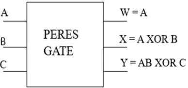
It is a 3 Input and 3 output gate which is shown in Fig. 1. The 3 inputs are considered as A, B, C and the 3 outputs are considered as W, X, Y. Peres gate is another important gate which has a low quantum cost as compared to other gates. Its quantum cost is four. Peres gate is a 3*3 reversible logic gate which is mostly used as a half adder by forcing the input variable C to zero thereby getting sum output from X and carry output from Y. Peres gate is composed of two XOR gates and one AND gate. Peres gate is universal logic gate and all the basic logic functions can be implemented using the Peres gate only. The Peres gate can be realized as the universal gate as all the basic gate functions can be implemented by Peres gate alone. A single Peres gate can give generate and propagate outputs when the third input C = 0.
[image:1.595.201.395.638.729.2]Table 1 Truth Table For Peres Gate
A B C W X Y
0 0 0 0 0 0
0 0 1 0 0 1
0 1 0 0 1 0
0 1 1 0 1 1
1 0 0 1 1 0
1 0 1 1 1 1
1 1 0 1 0 1
1 1 1 1 0 0
B. BME Gate
It is a 4 input and 4 outputs gate which is shown in Fig. 2. The 4 inputs are considered as A, B, C, D and the 4 outputs are considered as W, X, Y, Z and its quantum cost is five. BME gate is a 4*4 reversible logic gate. A BME gate is mainly used for generation of partial products in the multiplication process.
[image:2.595.74.512.118.262.2]Fig. 2BME gate
TABLE 2Truth table for BME Gate
A B C D W X Y Z
0 0 0 0 0 0 0 0
0 0 0 1 0 0 0 1
0 0 1 0 0 1 1 1
0 0 1 1 0 1 1 0
0 1 0 0 0 0 0 1
0 1 0 1 0 0 0 0
0 1 1 0 0 1 1 0
0 1 1 1 0 1 1 1
1 0 0 0 1 0 0 0
1 0 0 1 1 0 1 1
1 0 1 0 1 1 1 1
1 0 1 1 1 1 0 0
1 1 0 0 1 1 0 0
1 1 0 1 1 1 1 1
1 1 1 0 1 0 1 1
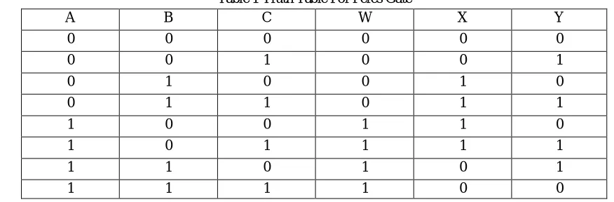
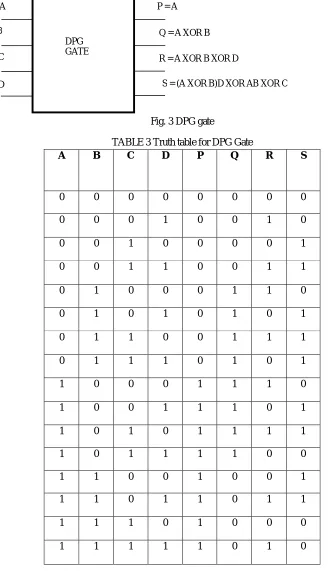
[image:2.595.172.431.334.472.2]C. DPG Gate
DPG gate is a 4 input and 4 output gate which is shown in Fig. 3. The 4 inputs are considered as A, B, C, D and the 4 outputs are considered as W, X, Y, Z and its quantum cost is six. DPG Gate is a 4*4 reversible logic gate. The reversible DPG gate can work singly as a reversible full adder. The proposed reversible multiplier circuit using DPG gate can multiply two 4-bits binary numbers.
Fig. 3DPG gate
TABLE 3 Truth table for DPG Gate
A B C D P Q R S
0 0 0 0 0 0 0 0
0 0 0 1 0 0 1 0
0 0 1 0 0 0 0 1
0 0 1 1 0 0 1 1
0 1 0 0 0 1 1 0
0 1 0 1 0 1 0 1
0 1 1 0 0 1 1 1
0 1 1 1 0 1 0 1
1 0 0 0 1 1 1 0
1 0 0 1 1 1 0 1
1 0 1 0 1 1 1 1
1 0 1 1 1 1 0 0
1 1 0 0 1 0 0 1
1 1 0 1 1 0 1 1
1 1 1 0 1 0 0 0
1 1 1 1 1 0 1 0
DPG GATE A
B
P = A
Q = A XOR B
C
D
R = A XOR B XOR D
[image:3.595.116.445.174.745.2]D. CNOT Gate
The most commonly used two input gates is the CNOT gate which is known as controlled NOT gate, essentially a reversible version of an EXOR. You can all that a 2-input Feynman gate. It is a 2-Input and 2-Output gate which is shown in Fig. 4. The 2-input are considered as A and B and the 2 Outputs are considered as C and D. The output of the CNOT gate corresponds to the results of a classical XOR gate. Its quantum cost is one. CNOT gate is required to copy the desire outputs and perform EXOR operations.
Fig. 4 CNOT gate
TABLE 4Truth table for CNOT gate
A B W X
0 0 0 0
0 1 0 1
1 0 1 1
1 1 1 0
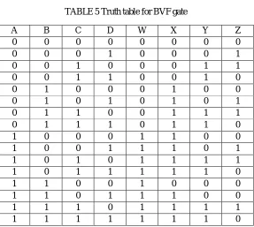
E. BVF Gate
[image:4.595.226.376.403.483.2]It is a 4 input and 4 output gate which is shown in Fig. 5. The 4 inputs are considered as A, B, C, D and the 4 outputs are considered as W, X, Y, Z and its quantum cost is two. It also referred as 4*4 bit double XOR reversible gate. This can be used for duplication of the required inputs to meet the fan-out requirements. BVF gate can be used as a fan-out gate with B = 0 and D=0.
[image:4.595.156.443.484.741.2]Fig. 5 BVF gate
TABLE 5 Truth table for BVF gate
A B C D W X Y Z
0 0 0 0 0 0 0 0
0 0 0 1 0 0 0 1
0 0 1 0 0 0 1 1
0 0 1 1 0 0 1 0
0 1 0 0 0 1 0 0
0 1 0 1 0 1 0 1
0 1 1 0 0 1 1 1
0 1 1 1 0 1 1 0
1 0 0 0 1 1 0 0
1 0 0 1 1 1 0 1
1 0 1 0 1 1 1 1
1 0 1 1 1 1 1 0
1 1 0 0 1 0 0 0
1 1 0 1 1 1 0 0
1 1 1 0 1 1 1 1
III. PROPOSED WORK
A. Reversible 4*4 Urdhva Tiryakbhayam Multiplier
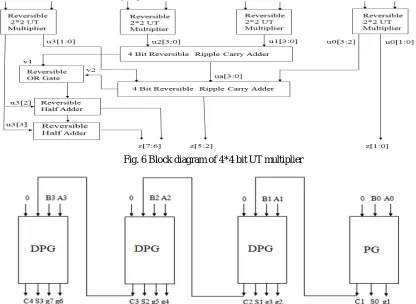
[image:5.595.85.501.297.601.2]Reversible 2*2 bit UT multiplier acts as input to the reversible 4*4 bit UT multiplier. Four blocks of 2*2 bit reversible UT multipliers are taken as inputs and inputs for first 2*2 bit UT multiplier are t[1:0], s[1:0]. The inputs of second multiplier are t[1:0], s[3:2]. The inputs of third multiplier are t[3:2], s[1:0]. The inputs of fourth multiplier are t[3:2], s[3:2]. The outputs of second and third 2*2 reversible UT multipliers are giving to the upper 4-bit reversible ripple carry adder. The MSB bits of first 2*2 bit reversible UT multiplier and LSB bits of fourth 2*2 bit reversible UT multiplier are given as inputs to the lower 4-bit reversible ripple carry adder(u0[3:2], u3[1:0]). The output of upper 4-bit reversible ripple carry adder is given as input to the lower 4-bit reversible ripple carry adder (ua[3:0]). The carry bits of upper and lower 4-bit reversible ripple carry adder is given to the Reversible OR Gate (v1, v2). The sum outputs of lower adder serve as the second, third, fourth and fifth bits of the final result (z[5:2]). The remaining bits of the final result (z[7:6]) is obtained by using two reversible half adders. In the implementation of reversible ripple carry adders DPG gate is used as a reversible full adder. For 4-bit reversible ripple carry adder requires 4-DPG gates as shown in Fig. 7 and Peres gate is used as a reversible half adder when the third input of the gate is zero as shown in Fig. 8 and RMUX1 gate can be used as reversible OR gate when the second input of the gate is zero as shown in Fig. 9.
Fig. 6 Block diagram of 4*4 bit UT multiplier
Fig. 7 Four bit Reversible Ripple Carry Adder using DPG and PG gates
Fig. 9 Reversible OR Gate
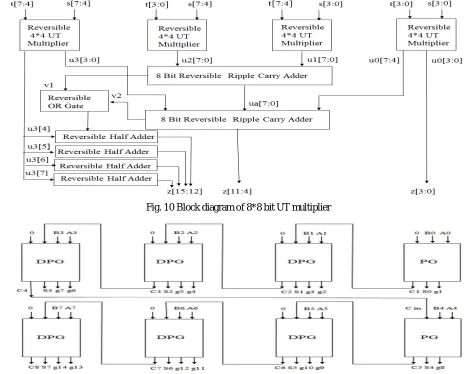
B. Reversible8*8 Urdhavatirya Kabhayam Multiplier
[image:6.595.60.528.365.739.2]Reversible 4*4 bit UT multiplier acts as input to the reversible 8*8 UT multiplier. Four blocks of 4*4 bit reversible UT multipliers are taken as inputs and inputs for first 4*4 bit UT multiplier are t[3:0], s[3:0]. The inputs of second multiplier are t[7:4], s[3:0]. The inputs of third multiplier are t[3:0], s[7:4]. The inputs of fourth multiplier are t[7:4], s[7:4]. The outputs of second and third 4*4 bit reversible UT multipliers are giving to the upper 8-bit reversible ripple carry adder. The MSB bits of first 4*4 bit reversible UT multiplier and LSB bits of fourth 4*4 bit reversible UT multiplier are given as inputs to the lower 8-bit reversible ripple carry adder(u0[7:4], u3[3:0]). The output of upper 8-bit reversible ripple carry adder is given as input to the lower 8-bit reversible ripple carry adder (ua[7:0]). The carry bits of upper and lower 8-bit reversible ripple carry adder is given to the Reversible OR Gate (v1, v2). The sum outputs of lower adder serve as the four, five and up to eleven (z[11:4). The remaining bits of the final result are (z[15:12]) is obtained by using four reversible half adders. In the implementation of reversible ripple carry adders DPG gate is used as a reversible full adder. For 8-bit reversible ripple carry adder requires 8-DPG gates as shown in Fig. 11.
Fig. 10 Block diagram of 8*8 bit UT multiplier
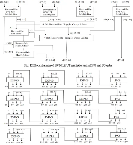
C. Reversible 16*16 Urdhva Tiryakabhayam Multiplier
[image:7.595.71.514.251.732.2]Reversible 8*8 bit UT multiplier acts as input to the Reversible 16*16 bit UT multiplier. Four blocks of 8*8 Reversible UT multipliers are taken as inputs and inputs for first 8*8 UT multiplier are t[7:0], s[7:0]. The inputs of second multiplier are t[15:8], s[7:0]. The inputs of third multiplier are t[7:0], s[15:8]. The inputs of fourth multiplier are t[15:8], s[15:8]. The outputs of second and third 8*8 bit reversible UT multipliers are giving to the upper 16-bit reversible ripple carry adder. The MSB bits of first 8*8 reversible UT multiplier and LSB bits of fourth 8*8 reversible UT multiplier are given as inputs to the lower 16-bit reversible ripple carry adder(u0[15:8], u3[7:0]). The output of upper 16-bit reversible ripple carry adder is given as input to the lower 16-bit reversible ripple carry adder (ua[15:0]). The carry bits of upper and lower 16-bit reversible ripple carry adder is given to the Reversible OR Gate (v1, v2). The sum outputs of lower adder serve as (z[23:8]). The remaining bits of the final result are (z[31:24]) is obtained by using eight reversible half adders. In the implementation of reversible ripple carry adders DPG gate is used as a reversible full adder. For 16-bit reversible ripple carry adder requires 16-DPG gates as shown in Fig. 13.
[image:7.595.78.511.253.455.2]Fig. 12 Block diagram of 16*16 bit UT multiplier using DPG and PG gates
IV. RESULTS AND COMPARISON
The proposed reversible UT multiplier designs are functionally verified through a logic simulation process. To perform simulation, test benches are created for the reversible UT multiplier designs. The Verilog HDL is used to code the designs. The simulation is carried out using Cadence Incisive simulator tool. Both Fig. 14 and Fig. 15 show the simulation waveforms for reversible 8*8 bit and 16*16 bit Urdhva Tiryakbhayam multipliers.
TABLE 6Performance comparisons of Reversible 4*4 bit UT Multipliers
Parameters 4-bit
Existing design [2] Proposed design
Number of gates 37 31
Constant inputs 29 31
Garbage outputs 62 38
Quantum cost 162 124
TRLIC 290 224
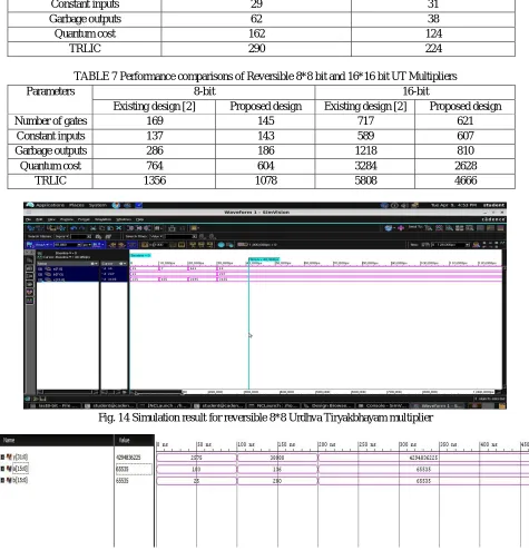
TABLE 7 Performance comparisons of Reversible 8*8 bit and 16*16 bit UT Multipliers
Parameters 8-bit 16-bit
Existing design [2] Proposed design Existing design [2] Proposed design
Number of gates 169 145 717 621
Constant inputs 137 143 589 607
Garbage outputs 286 186 1218 810
Quantum cost 764 604 3284 2628
TRLIC 1356 1078 5808 4666
[image:8.595.60.535.244.738.2]Fig. 14 Simulation result for reversible 8*8 Urdhva Tiryakbhayam multiplier
V. CONCLUSION
In this paper, Urdhva Triyakbhayam based multiplier, which is a formula of Vedic mathematics, was designed using reversible logic gates and simulated using Cadence Incisive simulator. The obtained results of proposed reversible 4*4, 8*8 and 16*16 UT multipliers are compared with the existing reversible UT multipliers. Finally, it was concluded that the proposed multiplier using reversible logic gates gives reduction in the number of gates, garbage outputs, quantum cost and TRLIC. In future, the proposed UT multiplier can be used in MAC design, filter design, DSP and other low power VLSI applications.
REFERENCES
[1] R. Arun Sekar and S. Sasipriya, “Implementation of FIR filter using reversible modified carry select adder”, Concurrency Computat Pract Exper, pp. 1-9, July 2018.
[2] T. R. Rakshith and Rakshith Saligram, “Design of High Speed Low Power Multiplier using Reversible logic: A Vedic Mathematical Approach”, International Conference on Circuits, Power and Computing Technologies, pp. 775-781, 2013.
[3] H. Thapliyal and M. B. Srinivas, "Novel Reversible Multiplier Architecture Using Reversible TSG Gate", Proceedings of IEEE International Conference on Computer Systems and Applications, pp. 100-103, March 2006.
[4] M. Shams, M. Haghparast and K. Navi, “Novel reversible multiplier circuit in nanotechnology”, World Appl. Sci. J., vol. 3, no. 5, pp. 806-810.
[5] Somayeh Babazadeh and Majid Haghparast, "Design of a Nanometric Fault Tolerant Reversible Multiplier Circuit", Journal of Basic and Applied Scientific Research, vol. 2, Jan. 2012.
[6] H. Thapliyal, M. B. Srinivas and H. R. Arabnia, “A Reversible Version of 4x4 Bit Array Multiplier with Minimum Gates and Garbage Outputs”, Int. Conf. Embedded System, Applications, Las Vegas, USA, pp. 106-114, 2005.
[7] H. Thapliyal and M. B. Srinivas, "Reversible Multiplier Architecture using TSG Gate", IEEE International Conference on Computer Systems and Applications”, pp. 241- 244, Mar. 2007.