Mark Westmijze
Memory optimizations on the sequential
hardware-in-the-loop simulator
Master’s Thesis by
Mark Westmijze
Committee: dr. ir. P.T. Wolkotte dr. ir. A.B.J. Kokkeler
ir. E. Molenkamp
i
Simulating hardware designs with the assistance of a Field-programmable Gate
Array (FPGA) can greatly increase the simulation speed. Especially since new
hardware designs often encompass a complete System-on-Chip (SoC). Due
to the limited resources of a single FPGAthese designs may be too large to
instantiate them into anFPGA. Wolkotte et al, presented a simulation approach
that can simulate those designs [1]. The approach uses time multiplexing to simulate only a small part of the hardware designs in a single clock cycle. This technique works well with hardware designs that contain a lot of nearly identical
components, e.g. a Multi Processor System-on-Chip (MPSoC). Such aMPSoC
may consist of a 2d-mesh Network-on-chip (NoC). Each router in theNoCcould
be connected to a small processing element, i.g. the Montium tile processor [2]. One of the transformations that is performed for time multiplexing the simulation is state extraction. The current approach by Rutgers [3, 4] is only able to extract flip-flops from the hardware designs. This thesis introduces some new algorithms that extract large memories. These algorithms make it possible to also simulate the network with the processing element attached. This was not possible in the approach of Rutgers due to the bandwidth limitations within
Abstract i
Contents ii
List of Acronyms v
1 Introduction 3
1.1 Related Work . . . 3
2 Hardware in the Loop Simulator 7 2.1 Overview . . . 7
2.1.1 Multiplexing Internal State . . . 7
2.1.2 Port Connections . . . 8
2.1.3 Evaluating all entities . . . 8
2.1.4 State Storage . . . 9
2.2 Current Status . . . 9
2.3 Research Definition . . . 9
2.3.1 State Access . . . 9
2.3.2 State Storage . . . 10
2.4 Outline Thesis . . . 11
3 State Access 13 3.1 Analysis Level . . . 14
3.2 Netlist Representation . . . 15
3.3 Memory Types . . . 16
3.4 RAMStructure . . . 17
3.4.1 Behavior . . . 17
3.4.2 Detection . . . 19
3.4.3 Extraction . . . 19
3.5 Register Bank Structure . . . 22
3.5.1 Detection . . . 22
3.5.2 Replacement . . . 33
4 State Storage 39 4.1 State Storage Hierarchy . . . 40
4.2 On chip State Storage . . . 40
4.3 Model . . . 40
4.4 Mathematical Model . . . 42
4.4.1 Input . . . 42
4.4.2 Output . . . 43
4.4.3 Constraints . . . 43
4.4.4 Minimize . . . 44
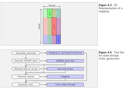
4.4.5 Example mapping . . . 45
CONTENTS iii
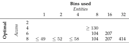
4.5 Tool Flow . . . 45
4.6 Initial AIMMS Results . . . 45
4.7 AIMMS Model Modification . . . 46
4.8 Minimum Bound . . . 47
4.9 Heuristics . . . 47
4.9.1 Naïve . . . 47
4.9.2 Merging . . . 47
4.9.3 Small First Merging with Padding . . . 48
4.9.4 Large First Merging with Padding . . . 48
4.10 Heuristics Results . . . 48
5 Implementation 53 5.1 State Storage Component . . . 54
5.1.1 MPRAMcomponent . . . 54
5.1.2 Address map component . . . 55
5.1.3 Combine component . . . 56
5.1.4 Component generation . . . 56
5.2 State Storage Pipeline . . . 57
6 Case study: NoC 63 6.1 Looprouter . . . 64
6.2 Extracted State . . . 64
6.3 Looprouter test . . . 64
6.4 Looprouter Synthesis Results . . . 65
6.5 State Storage Pipeline Synthesis Results . . . 66
7 Conclusions 71 7.1 Conclusions . . . 71
7.2 Future Work . . . 71
A Proof of stabilization 75 A.1 Assumptions . . . 75
A.2 Proof . . . 75
A.3 Evaluation example . . . 76
B Precision’s Import, and Export 79 B.1 Formats . . . 79
B.1.1 Export format . . . 79
B.1.2 Import formats . . . 79
B.1.3 Evaluation . . . 80
B.2 Netlist Size . . . 80
C Implementation 83 C.1 Java Implementation . . . 83
C.1.1 Java Classes . . . 83
List
of
v
ASIC Application-Specific Integrated Circuit
CE Clock Enable
CLB Common Logic Block
CPU Central Processing Unit
DCM Digital Clock Manager
EDIF Electronic Design Interchange Format
FF Flip-flop
FPGA Field-programmable Gate Array
GPU Graphical Processing Unit
HC Hyper Cell
HCI Hyper Cell Input
HCO Hyper Cell Output
HILS Hardware in the Loop Simulator
HDL Hardware Description Language
IAR Input Address Read
IO Input Output
KB Kilo (210) Byte
Kb Kilo (210) bit
LUT Look-up-table
MPRAM Multiple PortRAM
MPSoC Multi Processor System-on-Chip
NA Not Available
NoC Network-on-chip
NPRAM n-portRAM
OA Output Address
PnR Place and Route
RAM Random Access Memory
RB Register Bank
RTL Register Transfer Level
SE State Element
SOP Sum of Products
VLIW Very Long Instruction Word
VHDL Very High Speed Integrated Circuit Hardware Description
Chapter
Intro
ducti
RELATED WORK 3
Only 2300 transistors were needed to construct the first commercially available microprocessor. They were used to build the Intel 4004, the first Central
Processing Unit (CPU), built by the Intel Corporation in 1971 [5].
Several years earlier, in 1965, Gorden E. Moore observed, that the number of transistors that could be placed on an integrated circuit, doubled almost every year [6]. For about ten years Moore’s law held. After that Moore adjusted it to double every couple of years [7, 8].
The latter trend continued, which means that, since the early days of integ-rated circuits, the number of transistors on chips surpassed the billion mark in 2008. An example of one of these billion transistor chips is the GT200 Graphical
Processing Unit (GPU) from Nvidia [9], featuring 240 cores. Furthermore one
of Intel’s own processors, the Quad-core Itanium Tukwila, has even broken the two billion transistor mark [10].
The last several years there seems to be an increase in the number of large multi-core chips. Examples of these are: The Cell architecture [11], which features nine cores; An Intel research project named the Tera-scale Computing Research provided an 80 core chip, but never went into commercial production [12, 13].
But not only the large high performance chips went from single to
multi-core. For embedded solutions,MPSoCare developed, which use a homogenous
or heterogenous architecture of embedded processors, which are connected
through aNoCs [13]. An example of such an architecture is the Annabelle chip
[14].
Developing these new architectures requires knowledge of the required performance of applications and algorithms on the new architectures. Therefore, the new architectures will have to be simulated. However, these simulations
can take a long time [1, 15, 4]. The Hardware in the Loop Simulator (HILS)
introduces a simulation technique that uses relatively inexpensive equipment to reduce the simulation time of new hardware architectures, it will be elaborated in section 2.
1.1
Related Work
A hardware design has to be thoroughly simulated before it can be put in production. There are many methods how a hardware design can be simulated. These methods range from behavioral simulations to timing-accurate post synthesis simulations. They will be discussed starting at the highest level of abstraction, slowly working to a lower level of abstraction.
A method that can simulate designs from the behavioral level to Register
Transfer Level (RTL) is SystemC [16]. SystemC consists of a set of class libraries
for C++, these libraries can be used to model the hardware design. Hardware
designs that are implemented in a Hardware Description Language (HDL) can
be simulated in simulators such as ModelSim [17]. When the simulation speed of the software simulators start to become a bottleneck, hardware assisted
simulations are necessary. A simple method is to use anFPGAto simulate the
hardware [18], but the sizeFPGAcan limit the amount of hardware designs that
can be simulated. SeveralFPGAs together can simulate larger hardware designs.
Several commercial products are also available such as Veloce from Mentor Graphics [20], and the Hardware Embedded Simulation accelerator from Aldec
use multipleFPGAs to simulate those designs. But the complete design does not
have to be instantiated completely. The design can be programmed partially
in anFPGA, and during runtime be reconfigured to simulate the complete
design [21]. Cadambi et al. present a method that uses anFPGAto program a
Very Long Instruction Word (VLIW) processor, called SimPLE, which is able to
efficiently execute parts of a hardware design [22].
Another method, which is more suitable for hardware designs that largely consists of the same components, is proposed by Wolkotte et al [1]. All state elements are removed from the design, which make is possible to time multiplex the simulation of a single clock cycle. This makes is possible to simulate large
hardware designs in a singleFPGA. A automated flow has been developed by
Chapter
Ha
rdw
a
re
in
the
Lo
op
OVERVIEW 7
2.1
Overview
This section gives an overview of the simulator design. Detailed information can be found in [1, 3, 4]
The simulation speed of a hardware design can be increased by using one
or moreFPGAs to execute the simulation [23]. This is because anFPGAcan be
tailored to the design, such that each clock cycle of theFPGAcorresponds to
a clock cycle in the simulation. A software simulation does need many clock
cycles on theCPUto simulate a single clock cycle of the simulation [4]. FPGAs
use reconfigurable logic to instantiate the hardware design, but the size of the
designs that can be instantiated within a singleFPGAis limited. A simple, yet
expensive, solution would be to use multipleFPGAs to instantiate the complete
hardware design. But for very large hardware designs the required number of
FPGAs might be too high or the connections between theFPGAs might result in
anIObottleneck. For both cases another solution is necessary.
A hardware design consists of several instances ofcomponents, which will
be calledentities. For example in a Quad-core microprocessor there are four
instances of a processor core, which is the component. The instances themselves represent the entities.
As mentioned before, many of the new and large hardware designs run multiple entities of the same component in parallel. Instead of simulating all those entities in parallel, it is possible to evaluate them sequentially for simulation purposes. Moreover, because all entities from the same component can now run on a single instance of that component, less hardware is necessary
to simulate this transformed design. In which case it fits in a singleFPGA. The
instance of the component that will run the entities from the hardware design
is called thehyper cell. See [4] on how these hyper cells are generated.
Figure 2.1 depicts the current simulator. The basics of this simulator are elaborated in the following sections.
2.1.1 Multiplexing Internal State
Essentially, all instantiated entities of a specific component in the parallel architecture are run on one instance of that component. However, all these entities have an internal state in the form of memory elements. It is therefore not possible to use an unmodified version of the component to simulate all the entities, because only a single instance of such an component cannot be used to simulate more of them sequentially.
All state elements in the hardware design are replaced with some logic, which emulates the behavior of the extracted state elements. The state itself is then stored outside the transformed component, but through the replacement logic it is still available to the component.
Theinternal stateof each entity is represented by an entity’sstate vector. The
state vector for each entity is stored in a memory designatedstate storage. The
State Sto rage Hyper cell Link Sto rage State State’
out we in address address out we in
entity vector old link vecto r old state vecto r
new state vector new link vector
Links
out in
= eq flag
address address 1 1 0 0 1 sel
Figure 2.1: State storage configuration
2.1.2 Port Connections
The new state vector, and the output of an entity are also influenced by its input ports. The input ports are connected to the output ports of other entities. Therefore, it is necessary to correctly supply each entity with the output of the connected entities in the parallel architecture. The output of each entity is
represented by alink vectorand is stored in a memory designatedlink storage.
The link vector and state vector together represent theentity vector.
2.1.3 Evaluating all entities
A clock cycle in the original hardware design is called a system clock cycle.
A system clock cycle consists of the evaluation of all separate entities, these
evaluations are calleddelta cycles. In each delta cycle the input ports of an entity
CURRENT STATUS 9
vectors on which an entity depends are stable, a complete system clock cycle has been evaluated.
2.1.4 State Storage
Because an entity may be evaluated multiple times, it is necessary to store the old state vector for each entity until the end of a complete clock cycle. The new state vectors are also stored during the system clock cycle. Therefore, the state storage stores both the old, and new state for the entire system in separate memories. At the end of a system clock cycle the roles of these memories switch, because the old state in the next system clock cycle was the new state in the current. Hence these memories display ping-pong behavior [3]. This behavior is implemented in figure 2.1 by the muxes in the state storage.
2.2
Current Status
Wolkotte et al, demonstrate that it is feasible to use anFPGAto do fast simulations
of large parallel designs [1, 15]. Rutgers made an effort to begin the automation of this simulation flow [3]. This tool was the foundation of the ‘Sequential hardware in the loop simulator’. Currently, only a limited number of features are implemented in this simulator.
First, only some memory components are extracted. These are mainly flip-flops, and latches. Hence larger memories such as Random Access Memory
(RAM) are not yet supported.
Second, the automated simulator has mainly been simulated, and not run
on the actualFPGAitself.
2.3
Research Definition
In order to define the scope of this thesis the actual problem needs to be defined properly. The following sections define some of the current problems that need to be addressed in order to implement a more efficient simulator.
2.3.1 State Access
As explained in section 2.1.1, the state vector represents the state of a specific entity that is simulated. Hence the size of this vector is directly related to the amount of memory present in such an entity. In a naïve solution this complete state vector has to be supplied to the hyper cell of the entity, when it is evaluated. This leads to some severe problems, namely:
Bandwidth The complete state of an entity is represented by the state vector.
The problem occurs, when we do have an entity with a large state vector, because for each bit in this state vector a dedicated input line is needed. Before an entity can be evaluated on a hyper cell, the state vector has to be loaded from state storage as fast as possible. Ideally, in one clock cycle, otherwise the pipeline of the simulator will stall, which results in performance penalties. The width of the state vector depends on the hardware design being simulated. But it can range from a few thousand
in the case of a small hardware design such as aNoC-router [24, 25] to a
The only way anFPGAcan directly read a large amount of memory in a single clock cycle is when the data is stored on the chip itself. For this there are two techniques.
The first technique is to use the storage capacity of the basic components
of a FPGA, the Look-up-table (LUT). In a typicalFPGAtheseLUTs can
store 16 bits, depending on the number of input ports of theLUT. These
LUTs are glued together by multiplexing logic to create a structure, which
behaves as a memory. The main disadvantage of this technique is that
it consumes a large amount of basic components. In XilinxFPGAs this
ram structure is calleddistributedRAM. TheFPGAused within this thesis
supports distributedRAMupto 1056Kb.
The second technique uses dedicated memory components in anFPGA.
These memory components do have a maximum input- and data port width. However, it is possible to use several in parallel to increase the amount of data, which can be accessed or stored in a clock cycle. A disadvantage is that typically these memory components do have a syn-chronous read port, whereas distributed ram does have an asynsyn-chronous read port, which imposes a overhead for the evaluation when a hyper cell has asynchronous memories. However, since this technique uses dedic-ated memory components, it doesn’t consume any other basic component.
In XilinxFPGAs these memory components are calledBlock RAM. Each
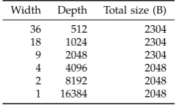
Block RAM stores 2304 bytes of information, and theFPGAthat is used as
target within this thesis houses 288 Block RAMs, which results in a total
storage capacity of 648KB. This limited amount of memory can lead to
another problem. For a hardware design that contains a lot of memory it
is possible that the amount of memory in anFPGAis not large enough to
accommodate the state and link storage. In that case the state, and link
storage has to be (partially) offloaded to memory outside theFPGA. This
creates another set of problems.
State partitioning When both the state, and link storage are placed in external
memory, because it did not fit in theFPGA, the entity vector is copied to
theFPGAbefore evaluating the entity. The bandwidth available between
theFPGA, and external memory is limited. Therefore, if the state vector
becomes too large, the simulator will stall until the complete entity vector is available. This will reduce the speed of the simulator.
However, in most hardware designs only a small portion of the current state vector changes or influences the new entity vector. The current state vector will still represent the complete current state of an entity, and the reduced current state vector will be a subset of this vector, which represents the part of the state, which influences the new entity vector. In the current naïve implementation this distinction is not made, and hence the complete state vector is loaded. The new state vector can be reduced in the same manner, because not all bits in the new state vector will change. Only the bits that might change, which depends on the current entity vector, do have to be updated.
Hence the first problem is:
How can we reduce the size of the old and new state vector?
2.3.2 State Storage
All the state vectors from all the entities represent thetotal system state. When
OUTLINE THESIS 11
design, but for performance reasons should be fetched in as few clock cycles as possible and ideally with a fixed latency in order to reduce the complexity of the simulator pipeline.
When usingFPGAs, several storage containers are available, these include:
Distributed ram, Block RAM and external memory. The state storage can be divided and spread over these containers. Due to time constraints for this thesis the focus will be how to use the Block RAMs as efficiently as possible. Because
how the state storage is mapped onto the Block RAMs of theFPGAdetermines
how much resources are needed and also influences clock frequency. Hence the second problem is:
How can we efficiently store the state storage in theFPGA?
2.4
Outline Thesis
Chapter 3 describes the solution for the state vector reduction. It covers the type of memories that can be extracted, and how they can be extracted. It concludes with some results on the vector reduction.
How the extracted state can be stored as efficiently as possible is elaborated in chapter 4. First, a mathematical model is introduced, which can find the optimal mapping with respect to the number of memories necessary for the mapping. Second, some heuristics are introduced, which can also be used to find mappings, but may not find the optimal mapping. The chapter concludes with some results on the state storage.
When both the state vectors are reduced, and an efficient way of storing all the state vectors is known, the storage pipeline which is responsible for loading, and saving the state vector can be implemented. This is elaborated in chapter 5.
A small case study is performed on aNoC-router, the results can be found
in chapter 6.
Chapter
State
A
Abstract
In this chapter two techniques for reducing the entity vectors are presented, in order to efficiently simulate large hardware designs. The first technique detects, and extracts large memories, which are represented by clocked_ram primitives in the hardware graph. The second technique detects register banks. Each register bank is removed from the hardware graph, subsequently replaced by a clocked_ram primitive, and some supporting logic. This replacement behaves exactly as the original register bank, but because the replacement uses the clock_ram primitive to store the state it can be extracted by the first technique.
Outline
Synthesis
tool
Compile
Synthesize Export
HDL sources
In-memory design database
Synthesized edif Intermediate format Figure 3.1: Input
levels
Currently, the extracted state is exported as a bit vector, which implies that during the evaluation of an entity the complete vector has to be loaded and
saved. At this moment the state vectors are stored in Block RAMs on theFPGA
itself. For now anFPGA, the XilinxXC4VLX160, with 288 Block RAMs, is used
as target platform. Each Block RAM is a dual portRAMthat both support
read-and write actions, read-and has a maximum data port size of 36 bits, read-and is capable of storing 2304 bytes. Since the new state vector has to be saved in the same clock cycle as the old state vector has to be loaded, only half of the total number of ports are available for either action. This results in a maximum bandwidth of 10368 bits per clock cycle per action, when all the Block RAMs are used for state storage. However, since the Block RAMs are also used for the link memories and other parts of the simulator, the actual bandwidth is smaller. For a small hardware design the required bandwidth suffices, but when the hardware design requires more bandwidth than available, the pipeline has to stall, and this will reduce performance of the simulator.
3.1
Analysis Level
All hardware designs, that eventually will result in anASIC, will have to be
processed in a few steps. The hardware design is initially represented in a
HDL, such asVHDLor Verilog. In the first phase of the synthesis flow aHDL
design is read, and compiled into technology independent components. The second phase consists of mapping these technology independent components into technology dependent components. The result of the synthesis is a netlist
that can be saved in the Electronic Design Interchange Format (EDIF), a netlist
is a file that describes all components of a hardware design, and how they are connected [26]. Compilation, and synthesis is usually done within a single tool, but some tools can also export the netlist between these two phases [27, 28]. A graphical overview of the levels, and how they are related is depicted in figure 3.1. These different levels, of which one will be chosen to be used within this thesis, are elaborated in the following paragraphs.
SynthesizedEDIF TheEDIFformat is a standard format for the interchange of
electronic designs between different tools [29]. Within this project there are two synthesis tools available, Synopsis [27] and Precision [28], that deliver netlists. But since these use the same technology library, both tools are elaborated as one option. The major disadvantage is that the used technology library does not
supportRAMcomponents with asynchronous read ports. Hence aRAM, with
NETLIST REPRESENTATION 15
are more complex to extract. An advantage is that, when the synthesis target
is a XilinxFPGA, the components that are used are thoroughly documented by
Xilinx.
Precision’s intermediate format As mentioned before most synthesis tools do
have two distinct phases. Between these two phases the hardware is described by a netlist that uses technology independent components. An example of such a component in the Precision tool is the clocked_ram component. The clocked_ram component is used as memory component for all types of memory configurations. The component itself functions as a memory with synchronous write ports, and asynchronous read ports.
The major advantage is that, because this component is used as basis for all large memories, when this component is extracted, all large memories are extracted. The major disadvantage is that Precision is not able to import the exported files directly before the second phase. However, these shortcomings
have been circumvented by exporting the netlist to VHDL, which made it
possible to compile. Another disadvantage is that the technology independent components are not documented. Since these components are relatively simple (e.g. asynchronous memory, muxes, selects, incrementors, multipliers, etc), it is not infeasible to determine the functionality of these components, after they can be simulated correctly.
Synopsys intermediate format Synopsys also uses an intermediate format
before the actual technology mapping. While the documentation suggests that it can infer asynchronous memories, this resulted in several internal errors within the compiler of Synopsys, and was therefore not usable. Because Synopsys did not infer these asynchronous memories correct, no effort was put into determining the source of these internal errors.
VHDL All the techniques mentioned above extract the ram after phases in
the synthesis flow. Because all these synthesis tools have the ability to detect
memory components, it should also be possible to write a VHDL analyzer.
ThisVHDLanalyzer should then be able to detect memory components, and
extract them at theVHDLlevel. For the analysis there is a parser available [30].
However, even using this parser the analysis ofVHDLproved to be too complex,
and is not further examined within this project. Another disadvantage ofVHDL
is that it does not cover all hardware designs, i.e. designs written in otherHDLs
cannot be analyzed.
Evaluation Precision’s intermediate format was chosen for the level to perform
the analysis, and transformations. Detailed information on which file formats are used for exporting, and importing this intermediate format can be found in appendix B.1. The most important advantage of this level is that it is technology independent.
3.2
Netlist Representation
The netlist describes the functionality of the design by an interconnection of primitive, and operator components. In the intermediate stage there are two libraries, primitives, and operators. These two libraries are used to determine the behavior of the component (See page 18).
We represent each primitive by a small graph in which the primitives function and each port is represented by a vertex. Each vertex of a primitive
Graphs representing such instances, are defined as:
Letp∈P be a component with input portsI[p]and output portsO[p]. A
primitive graphis defined asgp= (Vp, Ep, Lp, Bp), wheregpis a directed graph
that representspand
• Vp=I[p]∪O[p]∪ {p}is the set of vertices (also callednodes) in the graph,
wherepis a vertex that represents the primitivep;
• Ep ={i∈ I[p] | hi, pi} ∪ {o ∈ O[p] | hp, oi} is the set of edges in the
graph;
• Lp(v∈Vp)is a function that assigns a label to every vertex, such that
Lp(p)is a label based on the primitive of pandLp(v∈I[p]∪O[p])is
based on both the primitive ofp, and the label of the corresponding port.
• Bp(v∈Vp)is a function that assigns a library to every vertex.
The netlist is the hierarchical description of cells interconnected by wires. The instance of a component in a netlist is an example of a cell. Larger cells consist of multiple instantiated primitives and other cells. Each cell in the netlist is represented by a netlist graph in which vertices are uniquely described by their label and their hierarchical position (denoted with a sequence of numbers) in the corresponding netlist.
Thus, the graph of an instance of a primitive extends its primitives graph with such a hierarchy annotation on every vertex. The first number of this annotation corresponds to the cell number on the top level of the netlist, the second corresponds to the cell number within the top level cell, etc.
This netlist can be described as a graph:
Let c be a cell, built of instances of components Pc and other cells Cc,
with input ports I[c] and output portsO[c]. A netlist graph is defined as
gc= (Vc, Ec, Lc, Hc), wheregcis a directed graph that representscand
• Vc=I[c]∪O[c]∪Si∈Pc∪Cc{hLi(v), i:Hi(v)i |v∈Vi}is the set of vertices
in the graph;
• Ec=Wc∪Si∈Pc∪CcEiis the set of edges representing the wires in the
netlist, whereWc⊆Vc\Oc×Vc\Ic;
• Lc(v∈Vc)is a function that assigns a label to every vertex in the graph,
such thatLc(v) =Lp(v)whenv∈Vpfor a givenp∈Pc, otherwiseLc(v)
gives a label based on the portv∈I[c]∪O[c]it represents.
• Hc(v∈Vc)is a function that maps a vertex onto the hierarchical
annota-tion.
The combination of theLc(v)andHc(v)distinguishes every vertex in the
graph.
Graphical representation Figure 3.2 shows how a single primitive is depicted
graphically. The cell node is represented by the rectangle. The circular nodes represent the input-, and output ports.
3.3
Memory Types
RAMSTRUCTURE 17
a b c
o Cell
Figure 3.2: Primitive example
behavior of both memory structures is the same, but within the netlist they are represented in completely different ways.
• The first memory type, which is defined, is theRAM structure. It is
represented by a single primitive within the netlist. How this structure is detected and extracted can be found in section 3.4.
• The second memory type is the register bank, as the name suggests, it is an array of registers. The registers themselves are an array of flip-flops. This also means that this memory structure is not represented by a single primitive. Each flip-flop is a primitive, and other primitives are necessary to control the write enable signals, and the necessary logic to select values from the flip-flops. Section 3.5 elaborated the analysis, and extraction of register banks.
Before memory structures can be extracted they must be detected. This detection must not only detect primitives that together represent some memory structure, but also how this memory structure behaves, in order to simulate it correctly.
3.4
RAMStructure
In this section the analysis of theRAMstructure will be elaborated. First, the
behavior of such structures is presented. When the behavior has been analyzed, the structure can be detected in the hardware graph. In the last step the detected structure is replaced in the graph.
3.4.1 Behavior
As mentioned before, a memory element represents an array of values in which each value is separately addressable for read- and write actions. Typically, a memory element supports only synchronous writes. Therefore it will at
least have oneclockport. It is possible that multiple clock domains use the
same memory element. In that case multiple clock ports are present. Data can be retrieved and stored using address-, data- and write enable ports. An
addressport is responsible for addressing the location for the read, and or write
action. Aninputport is available for writing new data to the memory, but it is
only written when thewrite enableport is active. The data that is retrieved is
available at thedataport, or sometimes this port is referred to as the q port, if
theread enableis active. Ports do not necessarily support both the read- and
clocked_ram ram_new addr addr clk clk we we data data q q
(a) Asynchronous read
clocked_ram ram_new addr addr clk clk we we data data q q
(b) Synchronous read (Pipelined)
clocked_ram ram_new addr addr clk clk we we data data q q
(c) Synchronous read (WAR)
clocked_ram ram_new addr addr clk clk we we data data
q 0 q
1
(d) Synchronous read (RAW)
Figure 3.3: Examples of ram operator
Precision’sRAMimplementation In Precision’s intermediate format allRAM
structures are represented by theram_newoperator. However, this operator is
not a black box, it is further specified in the internal library operators, which is available within the netlist. The main component in this ram_new operator is theclocked_ramoperator. This operator implements the core function of theRAM
structure: Storing the data in a memory structure. Additional components such
as flip-flops, and muxes implement other parts of the functionality of theRAM,
such as a synchronous read port, read-after-write behavior , write-after-read
behavior, etc. See figure 3.3 for severalRAM structures in the intermediate
format.
Because of all the logic within the ram_new component it is not necessary to extract the complete ram component. It suffices to extract all the state components within it. The only state components in the ram component are flip-flops to store the output of the read ports, and the clocked_ram component to store all the data. How the flip-flops can be extracted can be found in [3].
Details of the clocked_ram operator As mentioned in the previous section
the clocked_ram component is a black box. In all configurations it behaves as a synchronous write, and asynchronous read memory component. It is used as the basic component for all memory storage. The behavior of the clocked_ram component depends on a few properties. Most of these properties are also available in the component’s identification string. An example of such an identification string is:
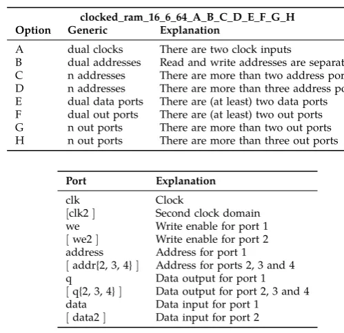
clocked_ram_16_6_64_F_F_F_F_F_F_F_F
The numbers respectively represent data width, address width, and the total number of locations. After the numbers are eight boolean options, see table 3.1 for the explanation of these options. The boolean values give information on which port this clocked_ram possesses, hence it is also possible to ignore the boolean option, and check the interface of the specific component for which
RAMSTRUCTURE 19
clocked_ram_16_6_64_A_B_C_D_E_F_G_H Option Generic Explanation
A dual clocks There are two clock inputs
[image:30.595.133.383.121.363.2]B dual addresses Read and write addresses are separated C n addresses There are more than two address ports D n addresses There are more than three address ports E dual data ports There are (at least) two data ports F dual out ports There are (at least) two out ports G n out ports There are more than two out ports H n out ports There are more than three out ports
Table 3.1:
Explanation of option booleans for clocked ram
Port Explanation
clk Clock
[clk2] Second clock domain
we Write enable for port 1
[we2] Write enable for port 2
address Address for port 1
[addr{2, 3, 4}] Address for ports 2, 3 and 4
q Data output for port 1
[q{2, 3, 4}] Data output for port 2, 3 and 4
data Data input for port 1
[data2] Data input for port 2
Table 3.2: Clocked
ram ports
It describes which of the ports are used for reading and writing, where the latter also can be deduced on the total number of write enable ports. However, also this behavior can be deduced based of the ports of the component. One last behavior to mention is that the clocked_ram component only triggers on the rising edge of the clock, and does not support dual edge triggering.
3.4.2 Detection
Clocked_ram components are represented by a single primitive. The label of the cell node for that primitive starts with ‘clocked_ram_’. The detection of clocked_ram components is therefore trivial.
3.4.3 Extraction
For the extraction of the clocked_ram only its input-, and output ports have to be connected to the outside. Replacement logic outside the hyper cell should fetch the required data for the input ports, and save data from the output ports to state storage.
In the intermediate graph format the implementation of this extraction is trivial, and not elaborated here.
ExtractedRAMbehavior Because the clocked_ram component uses an
asyn-chronous read, the data for that clocked_ram has to be available within the clock cycle that the entity is evaluated. Since the state is stored in Block RAMs that only support synchronous read actions, this is not possible Two techniques to circumvented this problem are multiple evaluations, and pipelined evaluation. In the following two paragraphs these techniques are elaborated.
Multiple evaluations The easiest solution to the asynchronous read
chain through two asynchronous memory elements can be detected. After the first evaluation the correct read address for ‘ram 1’ is available. Hence in the second evaluation the logic between ‘ram 1’ and ‘ram 2’, shown in the figure
as cloudG, derives the correct address for ‘ram 2’. In the third evaluation the
correct data is available for the output ports of both memories, and the state has stabilized.
This example shows that the number of evaluations necessary depends on the longest chain of asynchronous elements in the hardware design. The first technique used in the example determines the longest chain of asynchronous elements, and the scheduler has to evaluate the entity that amount of times after the last input change. The disadvantage of this solution is that some of its evaluations may be redundant, because the correct addresses already are available.
Another technique could compare the complete output of the hyper cell, and when the results of two consecutive evaluations are the same, and the input ports were the same, the state has stabilized. A disadvantage of this technique is that it requires one evaluation more in comparison with the first solution in the worst case, but when some of the addresses in the chain are already correct, the best case uses less evaluations than the first technique. Another disadvantage is that the comparison between the output of the current and last state may consume a lot of resources resources.
Therefore, a hybrid solution, which does count the evaluations, and also checks if the last two evaluations are the same may results in the least number of evaluations.
Pipelined evaluation Instead of multiple evaluations to fetch the correct
data, it is also possible to pipeline the hyper cell, so that a memory only fetches data at the moment that an address port has stabilized. The technique, which counts the number of evaluations that are necessary to stabilize a hyper cell, can be used to determine for each primitive when it has stabilized. All the primitives, which stabilize in the same clock cycle, are grouped together. See figure 3.4(b) for how the hyper cell from figure 3.4(a) would be divided. These groups can be used to implement a pipelined hyper cell. See figure 3.4(c) for the pipeline, which used the groups from figure 3.4(b); The advantage of this technique is that only one evaluation of the hyper cell is necessary. This reduces the bandwidth necessary to evaluate hyper cell. However, it does introduce a latency in the hyper cell, the new state is not available within one clock cycle.
Evaluation Because of the simplicity of the first technique, counting the
evaluations of the hyper cell, it has been chosen for implementation. However, implementing the pipelined technique could drastically improve performance, but this is left as future work.
Further optimizations The following paragraphs present some optimizations
that could further increase the simulation speed. These optimizations have not been implemented.
Synchronous read optimization Pipelining the hyper cell for
RAMSTRUCTURE 21
ram 1 ram 2
F G
H
I
entity
(a) Asynchronous elements chain
ram 1 ram 2
F G
H
I
(b) Separating prefetch example
Clk
Hyper
Cell
State
0 1 2
F G I
H
ram 1 ram 2
(c) Pipelined hyper cell
q
clocked_ram
(a) Before retiming
q
clocked_ram
(b) After retiming
Figure 3.5: Ram retiming
evaluations no data is fetched from state storage. Only at the end of the system clock cycle the data has to be fetched from state storage. As we can see in figure 3.3(b), 3.3(c) and 3.3(d) synchronous reads are implemented by placing a register after the output port of the clocked_ram. Hence if the output of the ram is only connected to flip-flops, the data does not have to be prefetched, because it is not actually used within the same clock cycle. So instead of an extra evaluation or pipeline stage, the address of the read location can be forwarded to the next clock cycle.
Synchronous read optimization through retiming When a ram is originally
implemented with asynchronous read ports, the hyper cell has to be pipelined or multiple evaluations are necessary. However, it might be possible to retime memory elements such that the output of the data port is directly connected to a synchronous write port, basically creating a synchronous read. See figure 3.5 for an example.
3.5
Register Bank Structure
Where the clocked_ram component represents a complete memory structure in a single primitive, register banks are made using multiple primitives. To be more specific the data is stored in flip-flops, the clock enables of those flip-flops are driven by addressing logic, and the correct data from the flip-flops is selected by muxing logic. All the primitives, which implement the flip-flops and the logic, which creates the register bank behavior together, represent
the register bank. Normally, when memories are described in theHDL, the
synthesis tool will correctly identify them asRAMstructures. But sometimes
they are not identified as memory, because for example clock gating is used, and in this case the memory structure is instantiated as register bank.
See figure 3.6 for a graphical example of how a register could look like. The register bank consists of several primitives, which can be divided into three groups that implement parts of the behavior of the register bank.
The core functionality of the register bank is data storage. This is done by the ‘state’ group, which consists of a group of flip-flop that are divided into
registers. The next group, the ‘CE-logic’ group, is responsible for which of the
flip-flops are enabled for writing, based on the address-, and we port. The last group, the ‘read logic’ group, selects the flip-flops that are being read by the read address port.
3.5.1 Detection
REGISTER BANK STRUCTURE 23
CE-logic State Read logic
addr2 reset addr we data clk 0 1 out clr clr in in clk clk q q ce ce
Figure 3.6: Register bank with two locations
Predefined search patterns For each known configuration of primitives
that behave as register bank, a search pattern can be defined. A search pattern consist of a group primitives, and how they are connected. An advantage of this technique is that it is simple to implement. However, this also has a downside, because only the predefined search patterns are extracted there can be no guarantee that all register banks are found. Furthermore, the configuration of known register bank configurations will already be enormous, matching all those search patterns on the graph will be time consuming.
Graph matching In essence the internal representation of the hardware is
a graph structure. This graph could be converted to a format, which can be imported in a graph matching, and transformation tool, such as Groove [31]. The idea is that the patterns specified in Groove are more general than the predefined patterns from the previous technique, and thus could recognize more register banks, with less predefined patterns. However, a small test with Groove showed that it is not powerful enough to express patterns that describe register bank behavior. Detecting register banks with multiple patterns is still feasible, but is nothing more than another way to express predefined search patterns.
CoSy pattern matching CoSy [32] is a compiler generation suite. Internally
it uses a graph like representation based on predefined building blocks. It could be possible to represent the hardware description in this format. Larger patterns, such as muxed/demuxed flip-flops, might be detected and extracted using the included pattern matcher. The major disadvantage is that the pattern matcher also expects predetermined search patters, and thus is yet another method to implement predefined search patterns. Another disadvantage is that the CoSy compiler has a closed source license.
Behavioral search Starting with some basic behavior of register and register
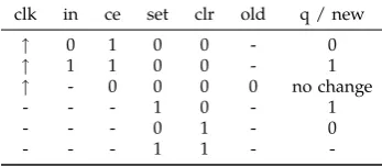
clk in ce set clr old q / new
↑ 0 1 0 0 - 0
↑ 1 1 0 0 - 1
↑ - 0 0 0 0 no change
- - - 1 0 - 1
- - - 0 1 - 0
- - - 1 1 -
-Table 3.3: Behavior
of flip-flop
large function, which operates on the entity vector. But this function basically describes when certain flip-flops should be written to, which flip-flops have influence on the output entity vector, and so on. Based on the behavior of this function, register bank behavior might be detected, and this behavior can be described mathematically. This is the major advantage of this technique; no search patterns need be defined, which could result in the detection of register banks, which were not known in advance. However, some small tests quickly showed that this technique uses too much processing time, when it has to take into account all of the combinatorial logic.
Evaluation The graph matching, and behavioral search techniques both
have some promising advantages. Both techniques try to detect register banks without defining the exact structure of what they are looking for. At this moment a hybrid solution of these techniques seems likely to give the best result. The small test with graph matching resulted in an easy way to detect groups of flip-flops that might belong to the same register bank, but much more than that was difficult to achieve without predefined patterns. But the combinatorial logic that was connected to these groups of flip-flops was a small subset of the graph, analyzing this subset with the behavioral search might be feasible without requiring much processing time. Therefore, a hybrid approach of graph matching and behavioral search is further elaborated in this section.
Register bank detection steps As mentioned before, the register bank
de-tection will be separated into several steps. A register bank consists of an array of registers, which themselves are arrays of flip-flops. First groups of flip-flops are detected by graph matching, these groups represent the registers in the hardware design. The registers are grouped again using another graph matching rule. These groups represent possible register banks. These groups will than be used to analyze a subset of the graph with a behavioral search to determine if the group of registers really does behave as a register bank. After this analysis can the register banks be removed, and replaced in the graph. These steps will be elaborated in the next paragraphs.
Flip-flop grouping First step is to identify the registers. Figure 3.7(a)
shows the graph representation of a flip-flop. This configuration is defined as the basic flip-flop. The behavior of other types of flip-flops can be emulated using this flip-flop and some additional logic. For example, a flip-flop without a clock enable can be seen as a basic flip-flop where the clock enable port is connected to logic ‘1’, as seen in figure 3.7(b) The same applies for flip-flops without a set or reset port. The behavior of the flip-flop can be found in table 3.3.
[image:35.595.237.411.127.203.2]REGISTER BANK STRUCTURE 25
in clk ce set clr
FF
q
(a) Basic flip-flop
TRUE
out
in clk ce set clr
FF
q
(b) Flip-flop without clock enable
Figure 3.7: Flip-flop configurations
This can be described formally. First letSbe the set of all possible states of
the hardware described by the graph, which is the Cartesian product of the
possible states of all state primitives. LetP be the set with all primitives of the
graph. Two flip-flops act the same, if for all possible states the input on their control (clk-, ce-, set- and preset) ports is the same. The following function determines what the value is for a specific port on a primitive in a state:
Vi,p,s=The value for portifrom primitivepin states (3.1)
Furthermore, we need to express when a flip-flop belongs to a specific register:
Rf,r=Flip-flopf belongs to registerr (3.2)
Finally only the flip-flops in a graph need to be checked; Hence the ability to retrieve the type of a primitive is defined via:
Tp,t=The primitivepis of typet (3.3)
Lets first define the formula, which checks that two flip-flops,fiandfj, act
the same way for a specific state s. In the following formula the first two
arguments are the two flip-flops followed by a specific state. Basically the formula checks that in a specific state the value of the control ports of the flip-flop have the same values. When they all have the same value, they will act the same.
Ffi,fj,s= (Vce,fi,s=Vce,fj,s
∧Vset,fi,s=Vset,fj,s
∧Vclr,fi,s=Vclr,fj,s
ce set clr clk
FF
ce set clr clk
FF
6
= Figure 3.8: Two
flip-flops belong to the same register rule
We use this formula, so that it does the check all possible states:
Gfi,fj =∀s∈S•Ffi,fj,s (3.5)
This will result in groups of registers where flip-flops will all reset or set together. A relaxation of equation 3.4 could also determine that when one flip-flop does a set, and the other a reset it does exhibit the same behavior. The register that will be found will have initiation pattern other than only zeros or ones.
Ff0i,fj,s= (Vce,fi,s=Vce,fj,s
∧Vclk,fi,s=Vclk,fj,s
∧((Vclr,fi,s=Vclr,fj,s∧Vset,fi,s=Vset,fj,s)
∨(Vclr,fi,s=Vset,fj,s∧Vset,fi,s=Vclr,fj,s)) (3.6)
However, at the moment the equation 3.4 is used within this thesis. Now we can express that, when two primitives are both flip-flops, and act the same way in all states, they belong to the same register.
∀pi, pj∈P|Tpi,FF∧Tpj,FF =⇒ (Gpi,pj =⇒ Rpi,r∧Rpj,r) (3.7)
REGISTER BANK STRUCTURE 27 in ce FF q in ce FF q in ce FF q
(a) Detected registers
Register in ce q in ce q in ce q
(b) Merged cell nodes
Register ce in q in q in q
(c) Removed redundancy
Register ce in0 q0 in1 q1 in2 q2
(d) Bus transformation
Figure 3.9: Flip-flops to register
transformation
Flip-flop merging All detected register groups can now be merged together
into registers. Figure 3.9(a) shows an example of a detected group of flip-flops. The set-, clk-, and clear ports have not been shown for simplicity. The cell nodes have been merged into the custom primitive ‘Register’ in figure 3.9(b).
For each group of flip-flops all cell nodes are merged into one new cell node, this cell node now represents a register, a custom primitive. Many of the ports connected to the merged cell node are redundant, hence ports with redundant behavior are removed. The redundant ‘ce-ports’ are still present at this step, and these are removed in figure 3.9(c). The last step involves changing all in-, and q ports to vector based ports, because they are now part of a bus. This final register is shown in figure 3.9(d).
FF FF FF FF
in in in in
q q q q
a b c d
(a) Example
FF FF
in in
q q
a b c d
(b) Transformed in in FF FF q q 6 = = (c) Transformation
Figure 3.10: Redundant flip-flops
In that case, the redundant flip-flop can be removed. The following function will check if one of the two flip-flops is redundant:
Ufi,fj = (fi6=fj∧(∀s:S|Vin,fi,s=Vin,fj,s)) (3.8)
The graph transformation rule, which does this is depicted in graph 3.10(c). This rule matches flip-flops of which one is redundant, the embargo node forbids them to be the same cell node. One of the flip-flops, including its in port is removed. Furthermore, the merge edge, annotated with the ‘=’, will merge both q ports, so that both original q ports will have the same value.
Register grouping At this moment the graph contains a set of registers,
a subset of these registers can form a register bank. The next step into the detection of register banks is to determine which of them can be grouped together. An important requirement for a register bank is that all registers receive the same data. At this moment the register bank detection is limited to register banks with a single write port. Hence all data in ports of the register banks will share an array of common nodes. Formally we can describe this in
a few steps. LetWi,pbe a function, which returns the set of ports for primitive
p, with labeli. When the specified input port is an array, all of its input ports
are present in this set. Furthermore, letXn be a function, which will return a
set which has all the predecessors of all the nodes in setnin it. Finally, let
Mr,b be a function which specifies that registerrbelongs to register bankb.
The following expression checks if two registers belong to the same register bank:
∀pi, pj∈P|TREG,pi∧TREG,pj∧XWin,pi =XWin,pj =⇒ Mpi,b∧Mpj,b (3.9)
The graph matching rule, which does the same thing is shown in figure 3.11. First it selects two registers, which cannot be the same register due to the embargo edge. Then it uses the universal quantifier to ensure that for all in ports there exist a common source node. When this graph rule matches on two registers, they belong to the same register bank. This graph will be used to group registers together that will form a register bank.
Register bank behavior analysis After the moment when several registers are
REGISTER BANK STRUCTURE 29
Register in
Register in ∃
∀
6
=
Figure 3.11: Data port matching
into a register bank. The analysis steps, which will be performed on the groups of registers are: Address logic detection, reset- and set detection, and read ports detection.
Address logic detection The clock enable inputs of a group of registers
are analyzed to see if they behave as a single write port. A group of registers behaves as a single write port if at most one of the registers is updated per
rising edge of the clock in all states. Therefore aClock Enable (CE)-graphfor the
group of registers is analyzed. TheCE-graph is defined as all the cells, which
influence the clock enables of the registers. This means that each node in the
CE-graph has a combinatorial path to one of the clock enables. First we define a
formula, which will determine if a specific node can influence the clock enable
ports of the register bank. The functionTstate,sis used to match all primitives
that have an internal state. In the following formula, letebe the set of clock
enables in a register bank,cbe the specific node andgbe the graph:
He,c,g=∃hs, ti ∈Eg|s=c∧ ¬Tstate,s∧(t∈e∨He,t,g) (3.10)
Using this equation all nodes can be checked to determine if they belong in
theCE-graph.
∀n∈Vg|He,n,g (3.11)
This graph has to be analyzed in order to determine where the address, and write enable signals are instantiated. The size of this graph might cover a large portion of the complete hardware graph. Hence the size of the entity vector, which has influence on the clock enables can be large as well. Determining for which input patterns a specific clock enable port is active can be solved
using theboolean satisfiability problem, which is NP-complete [33]. Hence many
of the clock enable graphs for the register banks, which were analyzed are too large to be analyzed directly. However, much of the information in the clock enable graph is redundant, and can be removed to simplify the detection of the addressing logic, which reduces processing time. The only primitives that
need to be in this influence graph are cells which ‘directly’ influence theCEs.
Nodes which do have more influence than at least one of their predecessors are identified as the new input ports. All of their predecessors are removed from the graph. First a new function is defined, which takes a node, all the clock enables, and a graph as arguments and returns the set of clock enable ports of that graph, which are connected to that node.
Ov,e,g ={∀e 0
∈e|H{e0},v,g} (3.12)
a b c d OR OR AND NOT x y (a) Original
a b c d
x,y x,y
x,y
x
x y
x, y⊆x, y x, y⊆x, y
x, y*x
x, y*y x⊆x
(b) Equation results
e
NOT
x y
(c) Reduced
Figure 3.12: Influence graph reduction example
∀v∈Vg|∃hs, ti ∈Eg•v=s∧Os,e,g6⊆Ot,e,g (3.13)
We illustrate this technique with a small example. See figure 3.12(a) for a small hardware graph with four inputs ports (a, b, c, and d), and two output ports (x, and y). For the set of inputs there are sixteen possible patterns. However, many of these patterns result in the same output values at the output ports.
See figure 3.12(b) for a graphical representation of how the last equation
is applied to the graph. In each cell node the result of the functionOv,e,g is
shown. At all the edges, the comparison of the influence of the two nodes is shown. In this graph it can be seen that the output port of the and-cell is identified as a new input port, because it has more influence on the output ports than any of its successors. Hence the output of this port becomes a new input port, reducing the number of input patterns from sixteen to two.
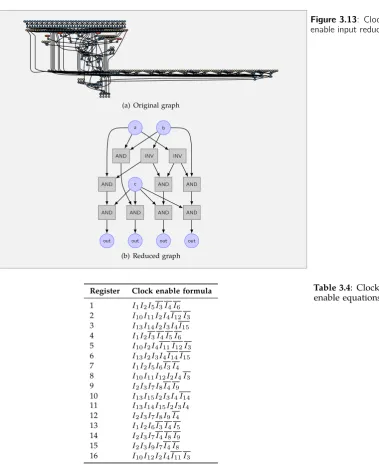
Figure 3.13(b) shows a reduced influence graph. The original graph, of which a portion is depicted in figure 3.13(a), has 40 inputs ports. After the reduction only three input ports remained. From the logic can be derived that input ports a, and b generate the address, and input port c acts as a write enable port.
Resolving mutual exclusiveness The resulting influence graph is
conver-ted to aprimitive influence graph. This graph should only contain the binary
operators and, or and the invertor as unary operator. Other operators such as a n-port and, or, etc operators are converted to binary operators.
For each output port its relation with the input ports is described in an equation. To ease the comparison of mutual exclusiveness the equations are
reduced to their minimal Sum of Products (SOP) equivalent. The ‘Boolean
REGISTER BANK STRUCTURE 31
(a) Original graph
a b
c
out out out out AND INV INV
AND AND AND
AND AND AND AND
(b) Reduced graph
Figure 3.13: Clock enable input reduction
Register Clock enable formula
[image:42.595.118.498.114.585.2]1 I1I2I5I3I4I6 2 I10I11I2I4I12I3 3 I13I14I2I3I4I15 4 I1I2I3I4I5I6 5 I10I2I4I11I12I3 6 I13I2I3I4I14I15 7 I1I2I5I6I3I4 8 I10I11I12I2I4I3 9 I2I3I7I8I4I9 10 I13I15I2I3I4I14 11 I13I14I15I2I3I4 12 I2I3I7I8I9I4 13 I1I2I6I3I4I5 14 I2I3I7I4I8I9 15 I2I3I9I7I4I8 16 I10I12I2I4I11I3
Table 3.4: Clock
enable equations
active at the same time. See table 3.4 for an example of these equations, the
equations are based a register bank found in theNoC-router.
Register
rst ∃ set
∀
Figure 3.14: Reset-and set detection
Reset- and set detection The registers within a register bank do have
reset-, and set ports. All the hardware designs that were analyzed during the development of the algorithm did either not reset their registers, or all in the same clock cycle. This led to the assumption that most register banks do reset or set all registers or none at all. It would be possible to extract register banks with selective reset or sets, but at the moment they will be discarded as register banks (See equation 3.4).
Therefore, a distinction must be made between these two types of register banks. As before with the detection of register banks, and data matching, we will determine if all reset- and set ports do have the same value in all states. The following expression must remain true, otherwise the register bank has to
be discarded. Let the setRcontain all register primitives in a register bank.
∀r∈R, s∈S|∃a∈ {0,1}, b∈ {0,1}|Vset,r,s=a∧Vreset,r,s=b (3.14)
This expression can be transformed to a graph matching rule; See figure 3.14 for the rule. The rule matches the registers that do have a common source for their reset- and set port. This rule should match all the registers in a register bank. If it does not match all registers there is not a common source for all registers, which implies that this register bank should be discarded.
Read ports detection On the read side of the registers we must identify
which registers are actually being read in a clock cycle. First the influence graph algorithm from the previous section was adapted to reduce the outgoing
graph. Equation 3.10 was rewritten to check if a node from the setq, has a
path to the current nodec, in the graphg:
Gq,c,g=∃hs, ti ∈Eg|t=c∧ ¬Tstate,s∧(s∈q∨Gq,s,g) (3.15)
Using this equation the outgoing graph can be defined as the graph with
the nodes from the following set, whereris the set of register cell nodes:
∀n∈Vg|Gr,n,g (3.16)
We determine which of the registers can have influence on the nodev:
Qv,r,g={∀r 0
∈r|G{r0,v,g}} (3.17)
Now we adapt equation 3.13, so that only nodes, which do have equal or less influence than all their successors, are included.
∀v∈VG|∃hs, ti ∈Eg•v=t∧Qt,r,g 6⊆Qs,r,g (3.18)
The outgoing graph is the graph with all nodes between the set of registers,
REGISTER BANK STRUCTURE 33
reduction, which was observed in theCE-graph. The outgoing graphs were, in
almost every case, too large to be processed by the Boolean Expression Reducer. However in all outgoing graphs the outputs of all the registers were muxes. Because only this structure was found, the predefined search pattern technique, as mentioned in section 3.5.1, was used.
The structure must meet several requirements, namely:
Only muxes All registers only drive muxes. When a register does not drive
a mux, it is possible that it always used. Further analysis, with for example a depth limited behavioral search, could still find muxing behavior in these components, but these structures are disregarded at this point.
First we define the following function that will return all successors for node
vat depthd:
Yv,d,g=
(
v d= 0
∀hs, ti ∈Eg|s=v|Yt,d−1,g d >0
(3.19)
Using this equation we can check whether there are cell nodes directly connected to the output of the registers that are not muxes. Because there is always an output- and an input port between two adjacent cell nodes, we look at all successors at depth 3 from the register cell nodes:
@r∈R|∃v∈Yr,3,g|¬Tmux,v (3.20)
Mux inputs When the input of the muxes only consists of the outputs of
the registers within the register bank, they are easy to extract. All muxes, found during the development of the register bank detection algorithm, complied to this. Hence the assumption is that most muxes, which are used by a register
bank, will only mux data from the register bank itself. LetM be the set of cell
nodes for the muxes as defined byYr,3,g. First we define a function, which will
return all predecessors at a certain depth, similar to the function in 3.19:
Zv,d,g=
(
v d= 0
∀hs, ti ∈Eg|t=v|Zs,d−1,g d >0
(3.21)
With this function we can check whether there are no inputs for the data
port of the mux, theaport, that are not connected to a primitive within the
register bank:
@m∈M|∃hs, ti ∈Eg|Ls=a∧Ys,2,g6⊂R (3.22)
Behavior analysis result When all analysis have confirmed the behavior
of the registers as a register bank it can be extracted. The register bank can be replaced by a properly configured clocked_ram component. How this this done can be found in the next section.
3.5.2 Replacement
Because the register bank behaves in the same way as a clocked_ram primitive,
it can be replaced by that. Then theRAMextraction, as explained in section
3.4, can be used to extract the clocked_ram primitive.
The register bank detection obtained the following information:
• Of allCEs, at most one can be active at the same time.
• The reset-, clk- and set ports for all registers share common sources. • The muxes connected to the data ports only mux data from the register
bank.
This information is used to implement the logic that is connected to the ports of the clocked_ram primitive.
clocked_ram instantiation A new cell node, with the label clocked_ram, is
added to the graph. Now all ports for the clocked_ram primitive need to be added, and connected to the graph. The following paragraphs describe how each of the ports is added, and what other logic is instantiated to correctly drive the ports.
clk port Because the clk ports of all registers share a common source, it
can be connected to a new port node with the label clk.
we port Only when one of theCEs is active the clock_ram is written to.
Hence a new OR primitive is added to the graph, the inputs of that primitives
are connected to theCEs.
addr[{ess,2,3, . . . ports}] These are the read ports of the clock_ram
prim-itive. They are connected to the address port of the muxes. Each register is annotated with the address of the input port of the mux that it is connected to. This information will later be used to correctly implement the write address port.
address port This is the write port of the memory. In the last step, when
the read ports are connected, each register was annotated with a read address. This information is used to correctly identify which clock enable belongs to
which address. Because theCEs signals, which form a sort of one hot encoded
address, do have to be converted to a normal address, which can be read by the clocked_ram primitive. A select-to-address primitive is added to the graph. This primitive performs that transformation.
data port The data port is directly connected to the data port of one of
the registers.
q[{2,3,. . . port}] For each set of muxes that form a read port, the outputs
of those muxes are connected to a new q port.
Reset- and set replacement Each register has a reset-, and set port. During
REGISTER BANK STRUCTURE 35
pipeline can be stalled and all locations can be updated sequentially. The disadvantage of this technique is that it imposes some timing overhead, how much depends on the frequency of (re)sets, and the depth of the register bank. Furthermore, it requires changes to the pipeline, in order to facilitate the sequential update.
The second solution keeps an additional reset vector, which buffers the reset and set signals. On the read side of the register bank this vector is accessed to see if the data can be read from memory or that a vector containing zeros or ones must be returned. When new data is written to the register bank the specific entry for that location is reset in the vector. The advantages of this solution are that no changes are necessary within the pipeline of the simulator (the required vectors can be instantiated within the logic of the hyper cell), and that it does not impose any timing overhead (on the assumption that the clock frequency does not increase). The disadvantage of this solution is that it imposes a memory overhead, because for every register in the register bank one or two flip-flops are necessary to store the reset-, and set signals.
The second solution was chosen, mainly because the implementation of it is simpler than the first solution.
Flip-flop insertion To store the set- or reset signal a flip-flop is added to
the graph for each location in the register bank. Each flip-flop reset port is
connected to one of theCE-signals, because when a specific location is written
to, that register it is no longer in its initial state. The set port for all the flip-flops are connected to either the reset- or set port from one of the registers.
Flip-flop selection When a location is being read from the register bank,
the flip-flop for that location has to confirm that the location is available for reading or that its initial state should be returned. One mux is inserted into the graph for each of the read ports, then the data ports for that mux are connected to the flip-flops, and the address port to the same signals that are used for the address read port.
Value or initialization selection Depending on the value of the flip-flop
selection mux the value from memory or an initialization vector should be returned. Therefore, a mux is inserted after the output port bits. These muxes selects either the data from the clock_ram primitive or the initialization vector, which at the moment is a vector of zeros or ones.
Primitive