Abstract—In this paper, we propose a multi-mode router, which supports three modes: bypass, bufferless and normal. By using the power gating technology, it can dynamically switch modes under different network loads, and effectively reduce the power consumption. Besides, in the bufferless mode, we propose an input priority judgment method and an output port allocation method to reduce the packet deflection rate. The experimental results show that compared with the basic wormhole router, the router working in the bypass mode can save nearly one hundred times power consumption with only 0.76% additional area overhead and the router working in the bufferless mode can save nearly 48.8% power consumption with 7.04% additional area overhead, that is, the proposed multi-mode router can meet the purpose of low power design and can adapt to the background of dark silicon.
Index Terms—Network-on-chip, multi-mode, dark silicon, router, power-gating technique1
I. INTRODUCTION
ecently, integrated circuit design is faced with a new problem called dark silicon, which means part of the cores on chip needs to be powered off to maintain the performance of multi-core system and not exceed the thermal design power. Taylor et al. [1] comprehensively introduced some current popular chip design schemes to cope with the negative effects brought by dark silicon phenomenon [2,3]. However, most prior studies focus on power-efficient core and cache optimization, while the design of dark-silicon-aware on-chip interconnect has not drawn much attention. In fact, Network-on-chip (NoC) [4] plays a vital role in message passing and memory access that directly influences the overall performance of multi-core processors. In NoC, the data exchange between cores is realized through the interconnection architecture composed of routers and
Manuscript received March 6, 2017.This work was supported in part by the Natural Science Foundation of China under Grant 61106018 and 61376025, the Natural Science Foundation of Jiangsu Province under Grant BK20160806, and the Fundamental Research Funds for the Central Universities under grant NS2016041.
Xintian Tong, the College of Electronic and Information Engineering, Nanjing University of Aeronautics and Astronautics(NUAA), Nanjing 210016, China (email:[email protected])
Fen Ge, the College of Electronic and Information Engineering, Nanjing University of Aeronautics and Astronautics(NUAA), Nanjing 210016, China (email: [email protected])
Rongrong Zhou, the College of Electronic and Information Engineering, Nanjing University of Aeronautics and Astronautics(NUAA), Nanjing 210016, China (email: [email protected])
Ning Wu, Fang Zhou, and Yingying Kong, are the College of Electronic and Information Engineering, Nanjing University of Aeronautics and Astronautics(NUAA), Nanjing 210016, China (email: [email protected], [email protected] , [email protected])
network interfaces, so when the dark silicon phenomenon occurs, the router connected with the powered-off core still need to keep working to prevent network congestion. Moreover, recent research results show that the power consumption of NoC can be up to 10% -36% [5,6,7], and most of it comes from routers. Therefore, the optimization design of NoC router becomes important for solving dark silicon problem.
Driven by these observations, in this paper, we carry out the research on the design of low-power NoC router in dark silicon era. The NoC router connected with the powered-off core is only the intermediate node in some routing paths, and is not involved in sending and receiving packets, so it can be powered off. However, the powered-off router has no routing function, and can block packet-forwarding. In order to prevent packet loss, in some studies, when there are some data packets pass through the powered-off router in the network, the current router will be woke up frequently by using power-gating technique [8,9,10], which will bring a large network delay and additional power consumption. Therefore, when the injection rate is low, we make the router connected with the powered-off core work in the bypass mode.
However, when the network injection rate increases gradually, the router working in the bypass mode may cause network deadlock or too much misrouting. Thus, the router needs to be configured to support routing function. While some studies show that the power consumption of the input buffer accounts for almost half of the router. Therefore, we propose to design a bufferless working mode. In recent years, due to the fact that the bufferless router can greatly reduce the power consumption of NoC, some research have been done in design bufferless router. A proposed bufferless router in [11] uses a simple permutation network instead of the serialized switch allocator and the crossbar to save nearly 48.8% power consumption. However, the router will bring unnecessary deflection of some packets. Therefore, the bufferless working mode we designed is based on deflection times and routing hops, and we propose an input priority judgment method and an output port allocation method to reduce the packet deflection rate. When the injection rate is larger, the packet deflection rate is higher, and the probability of livelock increases gradually, the router working in the designed bufferless mode can be switched to the normal working mode.
In this paper, in order to make the proposed router can be dynamically switched to three working modes, the PG controller module, the bypass module and the gated transistor module are added to the basic wormhole router, and the
Design of Low Power Multi-mode Router for
Network-on-chip in Dark Silicon Era
Xintian Tong, Fen Ge, Rongrong Zhou, Ning Wu, Fang Zhou, and Yingying Kong
arbitration allocation module is modified. The rest of the paper is organized as follows: Section II presents the structure of the proposed multi-mode router. Section III describes the switching method of three working modes and its implementation. Experimental results are demonstrated in section IV and we finally conclude our work in section V.
II. MULTI-MODE ROUTER DESIGN
The structure of the proposed multi-mode router is shown in Fig.1. It mainly includes PG controller module, bypass module, input and output modules, routing calculation module, arbitration allocation module and cross switch module.
Vdd
Gated transistor
GND gating signal PG1
East buffer
Local buffer
cross switch module (5×5) routing calculation
module
East output port
Local output port East input port
Local input port
Virtual Vdd2
Input port module
bypass module
Wake signal wu1 PG
controller
Vdd
Vdd
en gating signal PG2
gating signal PG3
Virtual Vdd1
Virtual Vdd3 Output
port module Wake signal wu2
[image:2.595.57.279.218.380.2]arbitration allocation module
Fig.1.The structure of the proposed multi-mode router
A.Bypass module
In the bypass mode, the incoming data packets are transmitted directly to the fixed output port through the bypass module, which has a fixed connection path between input and output port. The fixed connection path is set according to the location of the router in the network. When a router working in the bypass mode, the bypass module will be powered on and other routing modules will be powered off except the input and output port modules. In fact, only the packet coming from the direction of the fixed path can be forwarded to the corresponding output port, the other will be discarded and need to be resent from the source node again. When the extreme situation comes up that all routers have been switched to bypass working mode, we need to guarantee any two routers in the network can still communicate with each other to ensure the connectivity of the network. Therefore, we specify that the path to be chosen for each bypass module must be able to form a unidirectional ring connected to all nodes as shown in Fig.2. It can be seen from the figure that there are six types of fixed paths in the 2D Mesh NoC.
R4 R5 R6 R7
R12 R13 R14 R15
R8 R9 R10 R11
R0 R1 R2 R3
Fixed path 1 Fixed path 2
Fixed path 3 Fixed path 4
[image:2.595.352.502.321.428.2]Fixed path 5 Fixed path 6
Fig. 2.The fixed paths in the 2D Mesh NoC
B. Arbitration allocation module
In order to support the packet arbitration function of both bufferless and normal modes, the arbitration allocation module is modified. In addition to the original Round-Robin arbitration module, an input allocation module and an idle port deflection module are added to the arbitration allocation module.
1) Input arbitration module
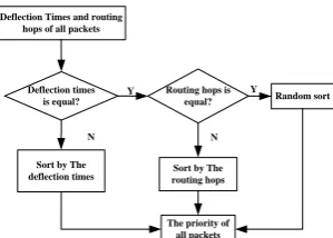
To judge the priority of the input packets, we propose an input priority judgment method which combines the deflection times and routing hops and is used in the input arbitration module. The algorithm flow chart of the judgment method is shown in Fig.3. The incoming packet has the highest priority if it has the highest deflection times. When deflection times are the same, then the one that has experienced the most routing hops gets the higher priority. This method ensures that the packet with the highest deflection times and experiences the longest time in the network has the highest priority and can be transmitted to the optimal output port.
Deflection Times and routing hops of all packets
Deflection times is equal?
Y
N
Routing hops is equal?
Sort by The deflection times
Y
N
Sort by The routing hops
Random sort
The priority of all packets
Fig.3.The algorithm flow chart of the input priority judgment method
Based on the proposed input priority judgment method, we divide the input arbitration module into three sub modules, namely, input priority judgment module, packet competition module and packet arbiter. The structure of the input arbitration module is shown in Fig.4. Firstly, the optimal output port of the packet coming from every direction that calculated by the routing calculation module will be input to the packet competition judgment module to get the competition results, which are used to detect whether there is any packet competition at the current cycle. Secondly, the deflection times and routing hops of the packet are input to the input priority judgment module to determine the priority of all packets with the above input priority judgment method. Finally, the priority of each packet and the competition results are input to the packet arbitration module to get the output ports for each packet, as well as the arbitration results for each packet and the idle output port set.
Input priority judgment module Routing hops
Packet competition module The optimal output
port of each packet
Packet arbiter The priority of
each packet Deflection times
Idle output port set Output port after arbitration
Competition
results Arbitration
[image:2.595.309.545.683.761.2]results
2) Idle port deflection module
The input packet which failed in the input arbitration module must select an idle output port in the idle output port set. In order to avoid excessive deflection, we propose a method for judging the idle output port priority. The algorithm flow chart of the method is shown in Fig.5. Due to the fact that the failed packet cannot be deflected to the local output port, we need only to calculate four priorities. As a matter of fact, the shortest path between the source node and the destination node is not unique, that is, the optimal output port is not unique. Therefore, we specify that the optimal output port own the highest priority and the value is 3, while the priority of the opposite direction output port is the lowest and the value is 0. Since the use of the deterministic XY routing algorithm, when the optimal output port is west or east, we need to compare the Y dimension address of the current node and the destination node which are stored in the head flit of data packet to get the priority of the north and south output ports. If the Y dimension address of the current node and the destination node are the same, then the priority of the north and south output ports are both 2. Otherwise, if the Y dimension address of the current node is bigger than the destination node, then the priority of north output port is higher than the priority of south output port, that is, the priority value of the north output port is 2 while the priority value of the south output port is 1. When the optimal output port is north or south, the priority of the west and east output ports are the same and the value are both 1.
the optimal output port, the Y dimension address of
the Current node and the destination node
the optimal output port is
east? Y
N
west:3, east:0
Y
Ycur=Ydest
Y N
north:2, south:2 Ycur>Ydest
N
Y
north:2, south:1 north:1, south:2
the optimal output port is west?
west:0, east:3
N
the optimal output port is
norh?
Y
north:3, south:0
N north:0, south:3
West:1, east:1
The priority of each output port Ycur:The Y dimension address of
the current node Ydest:The Y dimension address of
the destination address
1 2 3 0
Priority gradually increased
Fig. 5.The algorithm flow chart of output port allocation method
Based on the proposed output port allocation method, we divide the idle port deflection module into three sub modules, namely, deflection judge module, output priority calculator and idle port selector. The structure of the idle port deflection module is shown in Fig.6. Firstly, for an input packet, the arbitration result is input to the deflection judge module to know whether the packet failed in the input arbitration module. Secondly, the three parameters including the current node address, the destination node address and the optimal output port are input to the output priority calculator to get the priority of each output port by using the above output port allocation method. Finally, in combination with the idle
output port set, the selected output deflection port is output from the idle port selector.
Output priority calculator Current Node address
Destination Node address Optimal output port
Idle port selector Idle output port set
The priority of each port
Deflection port
[image:3.595.309.543.94.168.2]Deflection judge module Arbitration result
Fig.6.The structure of idle port deflection module
III. MULTI-MODE SWITCHING METHOD AND ITS IMPLEMENTATION
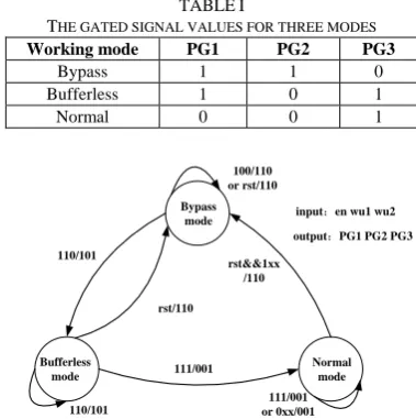
In order to support the proposed router to dynamically switched working mode under different network loads, three gating signals PG1,PG2 and PG3are generated by PG controller module to control the working state of some modules. The gating signalPG1 is connected with the input buffer module, the gating signalPG2 is connected with the other route modules, and the gating signalPG3 is connected with the bypass module. The gating signals and the modules are connected via the gated transistors, which are linked to the actual power supplyVdd. In addition, the input and output modules are directly connected with the actual power supplyVdd. The output value of the virtual powersVdd1,
2
Vdd , Vdd3 are determined by the value of the gating signals. We specify that the value 1 of gating signal represents the connected module is powered off. The values of the gating signals PGnin three working modes are shown in table I.
TABLEI
THE GATED SIGNAL VALUES FOR THREE MODES
Working mode PG1 PG2 PG3
Bypass 1 1 0
Bufferless 1 0 1
Normal 0 0 1
Bypass mode
Normal mode Bufferless
mode
input:en wu1 wu2
output:PG1 PG2 PG3
110/101
111/001 100/110 or rst/110
110/101
rst/110
rst&&1xx /110
[image:3.595.330.520.456.647.2]111/001 or 0xx/001
Fig.7.The state transition process of PG controller module
The PG controller module has three input signals, which are powered-off signal en and two wake-up signals
1
wu ,wu2. The value of en is determined by the working state of the connected core. If the core is powered off, the value ofenis 1, otherwise the value is 0. We use the state
working mode of the router is determined by the value of the powered-off signalen. The value of enis 0 means the initial working mode of the router is normal mode. On the contrary, when the value is 1, the initial working mode is bypass mode. After the initial working mode is determined, the working mode of the router at runtime is dynamically switched according to the wake-up signalswu1, wu2. We specify that only the router in the bypass mode will change the working mode according to the wake-up signals. It can be seen from the Fig.7 that the router working in the bypass mode (PGn:110) can be switched to bufferless mode only when the wake up signal wu1is valid (the value is 1, PGn:101 ), that is, the bypass module is powered off while the route module is powered on. When the signal wu2 is valid (the value is 1), the router working in the bufferless mode will be switched to the normal mode (PGn:001), which means the input buffer module will be powered on. In fact, once the reset signalrstturns to 1, the working mode will be switched according to the signalen, regardless the current working mode of the router.
In this paper, in order to support the packet arbitration function of bufferless and normal mode, we add a selecting signal enablein the arbitration allocation module to online strobe the arbitration function. The structure and state transition process of the arbitration allocation module is shown in Fig.8. As we can see from the Fig.8(a), the optimal output ports and routing information of all incoming packets should be input to the two arbitration modules at the same time, and two wake-up signalswu1,wu2 are input to the state machine to decide the arbitration mechanism the router used. Two wake-up signals wu1, wu2 are given in the section III. The arbitration results from the above two modules will be input to the output judgment module to determine the output ports that all packets finally choose.
Wake-up signal (wu1)
Wake-up signal (wu2)
State machine
enable
Round-Robin mechanism
the optimal output ports and routing information of all packets
Arbitration results
Idle output port set
=1
=0
Input arbitration module
Idle port deflection module
Output judgment module
Arbitration results
Output port selected for each packet
Deflection results Deflection arbitration module
(a) The structure of the arbitration allocation module
Round-Robin arbitration Deflection
arbitration
Input/Output wu1 wu2/enable 1x/1
or rst/1
x1/0 or rst/0 or 00/0 1x/1
x1/0
(b)The state transition process of the arbitration allocation module
Fig.8.The structure and state transition process of the arbitration module
In Fig.8(b) , the state transition process shows that, when the wake-up signal wu1 turns to 1, the selecting signal
enable will be 1, representing the deflection arbitration module based on deflection times and routing hops will be used as the part of the router. After that, when the value wu2 turns to 1, the selecting signal enable will change to 0, which means the Round-Robin arbitration module will be used. The switching processes of three modes are presented in details as follows.
A. Bypass mode dynamically switch to bufferless mode
In the bypass module, in addition to achieve the six types of fixed paths, a counter and a comparator are added to the module to get the wake-up signalwu1. The mode switching structure in the bypass module is shown in Fig.9. The counter records the number of data packets to get the packet injection rate. The packet injection rate and the set threshold are compared in the comparator to generate the wake-up signal wu1. Once the packet injection rate exceeds the threshold, indicating the utilization rate of the router is higher. At this time, if the router has been working in the bypass mode without routing function, it will bring excessive packet congestion and misrouting, eventually lead to deadlock. Therefore, we regard the output of the comparator as the wake-up signalwu1 to determine whether the router needs to be switched to the bufferless working mode. When the value of the signal wu1 is changed from 0 to 1, the state machine in the PG controller will be transformed, and the value of each gating signal will change too. Specifically, the value of the gating signal PG1 is still 1, while the value of the gating signal PG2turns to 0 from 1, andPG3 turns to 1 from 0, that is, the route module will be powered on while the other two modules (bypass module and input buffer module) will be cut off the power supply.
Wake-up signal wu1 Threshold
clock cycles
Injection rate Packet counter
Threshold comparator cnt1
East input port
local input port
Injection rate calculation
function
Fig.9. The mode switching structure of bypass module
B. Bufferless mode dynamically switch to normal mode
threshold are compared in the comparator to generate the wake-up signalwu2. Once the packet deflection rate exceeds the threshold, indicating too many packets deviate from the shortest path, which will bring excessive packet congestion and the probability of livelock increases. Therefore, we regard the output of the comparator as the wake up signalwu2 to determine whether the router needs to be switched to the normal working mode. When the value of the signal wu2 is changed from 0 to 1, the state machine in the PG controller will be transformed, and the value of each gating signal will change too. Specifically, the value of the gating signal PG1 turns to 0 from 1, while the value of the gating signal PG2 is still 0, and PG3is still 1, that is, only the bypass module will be cut off the power supply.
Wake-up signal wu2 Threshold clock cycles
Deflection rate Deflection
counter
Threshold comparator Arbitration result
cnt2 Deflection judge module
def
Deflection rate calculation function
Fig.10.The mode switching internal structure idle port deflection module
IV. EXPERIMENTAL RESULT
In order to get the thresholds used in the bypass module and the idle port deflection module, and to verify the function of the proposed multi-mode router, some experiments have been done. The experimental results are presented in this section.
A.Threshold estimation
We modified the Booksim simulator to construct a 4*4 Mesh NoC with our proposed multi-mode routers, and the network frequency is 1GHz. We specify the packet size is ten flits, and there are four virtual channels in the input buffer for each port. The depth of each virtual channel is eight flits, and the used routing algorithm is deterministic XY routing algorithm.
1) Threshold for bypass mode switching to bufferless mode
To get the threshold used in the bypass module, we configure a network as shown in Fig.11(a). The initial working modes of some routers (the router with grey color in the Fig.11(a) ) are set to be bypass mode because they may most likely to bring packet misrouting into the network (Worst case). The average network latency is shown in Fig.11(b). It can be seen that there is a sharp rise in the average latency after the packet injection rate is bigger than 0.06, which means the network is saturated. Therefore, the injection rate of 0.06 is chosen as the switching threshold used in the bypass module.
R1 R2
R4 R5 R6 R7
R12 R13 R14 R15
R8 R9 R10 R11
R0 R1 R2 R3
Bypass mode
Fixed path Normal mode
injection rate (flits/node/cycles) 0
A
v
er
a
g
e
la
te
n
cy
(c
y
cl
es
)
0.010.020.030.040.050.060.070.08 0.1 40.0
100.0
80.0
60.0 increase slow
81.3
48.7
0.09 51.7
47.1 52.0
57.7 66.6
72.0 106.1
sharp rise
189
(a) The configured network (b) Average network latency Fig.11.The network and the average latency
2) Threshold for bufferless switching to normal mode
To get the threshold used in the idle port deflection module, we configure a network (the working modes of the router R2 and R6 are both bypass mode, the router R0 is the source node and the router R3 is the destination node) as shown in Fig.12(a), which we found that with the increase of network injection rate, the network collapse time is the earliest ( Worst case). It can be seen that when R0 sends packets to R3, all packets pass through R2 and R6 will be deflected, so the injection rate of the network can be seen as the packet deflection rate. The average network latency is shown in Fig.12(b). It can be seen that there is a sharp rise in the average latency after the packet injection rate is bigger than 0.07. Therefore, the injection rate of 0.07 is chosen as the switching threshold used in the idle port deflection module.
R4 R5 R6 R7
R12 R13 R14 R15
R8 R9 R10 R11
R0 R1 R2 R3
source destination
Bypass mode
Fixed path Normal mode
Injection rate (flits/node/cycles) 0
A
v
e
r
a
g
e
l
a
te
n
c
y
(
c
y
c
le
s)
0.010.020.030.040.050.060.070.08 0.1 0.11 35.0
40.0 70.0
60.0
50.0
36.4 39.0
0.09 39.5
38.1 43.2
46.8 48.5
55.0 62.8
82.8148
sharp rise
(a) The configured network (b) Average network latency Fig.12. The network and the average latency
B.Functional verification
We use multi-mode routers to build a 4*4 Mesh NoC in the Modelsim simulation platform. The data packet in the network is usually made up of head flit and data flit and tail flit. In this paper, we specify that the size of each flit is 64bits. The packet format is shown in Fig.13. Each flit has 4bit network flag to mark the current network information. The head flit mainly consists of four parts: the deflection times of the packet, the total routing hops, the destination node address and the current node address, and the rest is reserved. In the next experiment, in order to facilitate the analysis, we specify each packet contains only one flit, that is, the reserved bits of the head are used as the date information.
Network flag
0 0 3 6 10 14 63
Deflection times
Total routing
hops
Destination address
Current
address Reserved
Head flit 64bit
4bit
Date flit/ tail flit
0 0 63
data
bit0:Link is valid? bit1:flit is valid?
3
3
bit2:is head flit? bit3:is tail flit?
Network flag
1) Functional verification of the multi-mode router
We configure a network as shown in Fig.14(a), router R6 working in the bufferless mode and routers R5, R9, R10 working in the bypass mode. Source nodes R14 and R7 both send packets to destination node R2 simultaneously. We can observe the transmission paths of the two communication tasks to verify the function of the network constructed by the multi-mode routers.
R4 R5 R6 R7
R12 R13 R14 R15
R8 R9 R10 R11
R0 R1 R2 R3
op2
R5\R9\R10:bypass mode;
R6:bufferless mode;
Task1:R14->R2;
Task2:R7->R2; Task1
Task2
op1
op3 op0
local Output port:
Source
Source desitination
(a) The network constructed by multi-mode routers
10
R7 R5 R9 R13 R14 R10 R6 R2
R14->R10 000_000
R7->R6 000_000
R10->R6 000_001 R6->R2 000_010 R6->R5 000_001
R5->R9 001_010
R9->R13 001_011
R13->R14 001_100
R14->R10 001_101
R10->R6 001_110
R16->R2 001_111
11 12 13 14 15 16 17 18 19 20 21 22 23 24 25 26 27 28
Ro
ut
er
Clock cycle(cycles) Deflection times + routing hops
Task 1
Task 2
(b) The transmission paths of the two communication tasks
Fig.14.The network constructed by multi-mode routers and the transmission paths of the two communication tasks
In Fig.14(b), we can see that at the rising edge of the tenth clock cycle, a packet of task one is generated from the local port of R14. After three clock cycles, the packet arrives at the output port op2 and is routed to R10. Since the working mode of R10 is bypass, the incoming data packet will be transferred directly to the fixed output port op2 through the bypass module and is routed to R6. Meanwhile, the packet of task two is transferred to R6 from R7, that is, R6 receives the packets of R10 and R7 simultaneously. As the Fig.14(b) shows that the packet form task one is transferred to the destination R2, while the packet form task two is deflected to R5, and the deflection times is updated to 3'b 001(deflection times and routing hops are both stored in the head flit of the data packet). The reason is presented below. According to the deterministic XY routing algorithm, the best output ports of the two packets are the north output port. Since R6 working in the bufferless mode, there is a packet must be deflected. According to the proposed input priority judgment method, when the deflection times of the two packets are zero, the packet with a larger number of routing hops from the task one gets the best output port and should be transferred to the destination R2, while the packet from task two should be deflected to R5.
2)Functional verification of three mode switching
In this experiment, the router R10 in Fig.14(a) is set to working in the bypass mode, and the other routers are set to working in the normal mode. The mode switching graphs is shown in Fig.15. From the previous section, we chose 0.06 to be the threshold used in the bypass module, that is, when there are on average six (3'b110) data packets coming within 100 clock cycles, the router need to be switched to bufferless working mode.
10 12 14 16 18 20 22 24 26 28
cnt1
Clock cycle(cycles)
1 2 3 4 5 6 7 8
30 9
001/0 010/0
011/0 100/0
101/0 110/0
000/1
cnt1/wu1
40 44 48 52 56 60 64 68 72 76
cnt2
Clock cycle(cycles)
1 2 3 4 5 6 7 8
80 001/0
010/0 011/0
100/0 101/0
110/0 111/0
cnt2/wu2
84 88 92 94 000/1
(a)Bypass to bufferless mode (b)Bufferless to normal mode Fig.15.The changes of cnt1 and cnt2 in router R10 during mode switching
We can see from the Fig.15(a), at the rising edge of the ninth clock cycle, the counter in the bypass module records the first packet, and the value of the corresponding signal
1
cnt is changed to 3'b001 while the value of wu1is still 0. At the rising edge of the twenty-sixth clock cycle, the value of
1
cnt is changed to 3'b110, representing the injection rate in the network reached 0.06. At this time, when there is a new packet pass through R10, the value of the wake-up signal
1
wu is set to 1, which means the R10 is switched to the bufferless working mode. From the Fig.15 (b), we can see at the rising edge of the eighty-fifth clock cycle, the counter in the idle port deflection module records the seventh deflected packet, so the value of cnt2 is changed to 3'b111, representing the deflection rate in the network reached 0.07. At this time, when there is a new packet being deflected, the wake-up signal wu2is set to 1, which means the R10 is switched to the normal working mode.
C.Overhead analysis
To evaluate the area and power overhead of our proposed multi-mode router, we synthesize the design using Synopsys Design Compiler in 180 nm technology. The overhead of each working mode router are shown in table II.
TABLEII
THE POWER CONSUMPTION AND AREA
Router Power consumption (mW)
Area overhead (mm2) Multi-mode router in
the bypass mode 2.10 5.3609
Multi-mode router in
the bufferless mode 126.54 5.6965
Basic wormhole router 247.04 5.3206
and the router working in the bufferless mode can save nearly 48.8% power consumption with 7.04% additional area overhead generated by the deflection arbitration module. It can be seen that the multi-mode router we proposed can meet the purpose of low power consumption design and can adapt to the background of dark silicon.
V. CONCLUSION
In this paper, we propose a multi-mode router for NoC in dark era, which supports three working modes, namely, bypass mode, bufferless mode and normal mode. In the bufferless mode, an input priority judgment method and an output port allocation method are proposed to reduce the packet deflection rate of the network. Moreover, we analyze the switching processes of the router and determine the switching thresholds. Experiment results show that our proposed router can save significant power consumption.
REFERENCES
[1] Taylor M B. Is dark silicon useful?: harnessing the four horsemen of the coming dark silicon apocalypse [C]. IEEE/ACM Design Automation Conference. 2012:1131-1136.
[2] Esmaeilzadeh H, Blem E, St. Amant R, et al, “Dark silicon and the end of multicore scaling,” international Symposium on Computer Architecture, vol.39, no.3, pp.365-376, 2011.
[3] Taylor M B, “Is dark silicon useful?: harnessing the four horsemen of the coming dark silicon apocalypse, ” in Proc. DAC, pp. 1131-1136, 2012.
[4] Ouyang Y M, Dong S Z, Liang H G, “Design and Simulation of NoC
Routing Algorithm Based on 2D Mesh,” Computer Engineering, vol.35, no.22, pp.227-229, 2009.
[5] Mattson, Timothy G., et al, “The 48-core SCC Processor: the Programmer's View,” in Proc. Conference on High PERFORMANCE
Computing Networking, Storage and Analysis, pp.1-11, 2010.
[6] Bell S, Edwards B, Amann J, et al, “Tile64-processor: A 64-Core SoC with Mesh Interconnect,” in Proc. IEEE International Solid-State
Circuits Conference, pp. 88-598, 2008.
[7] Hoskote Y, Vangal S, Singh A, et al, “A 5-GHz Mesh Interconnect for a Teraflops Processor,” IEEE Micro, vol.27, no.5, pp.51-61, 2007. [8] L. Chen and T. M. Pinkston, “Nord: Node-router decoupling for
effective power-gating of on-chip routers,” in MICRO-45,vol.90, pp. 270–281, 2012.
[9] Kitagawa, E., et al, “Impact of ultra low power and fast write operation of advanced perpendicular MTJ on power reduction for high-performance mobile CPU,” Electron Devices Meeting ,vol.48, pp.29.4.1-29.4.4,2012.
[10] Das, R., Narayanasamy, et al, “Catnap: energy proportional multiple
network-on-chip,” international Symposium on Computer
Architecture, vol.41, pp.320-331,2013.