A VLSI Array Architecture for Realization of DFT, DHT, DCT and DST
K. Maharatna*
System Design Dept.
Institute for Semiconductor Physics Technology Park 25
D-15236 Frankfurt (Oder) Germany
email: [email protected] FAX +49-335-5625671
A. S. Dhar and Swapna Banerjee
Dept. of E & ECE Indian Institute of Technology
Kharagpur - 721302 (INDIA)
email : [email protected] FAX +91-3222-55303 (* Author for correspondence)
Abstract :
An unified array architecture is described for computation of DFT, DHT, DCT and DST
using a modified CORDIC (CoOrdinate Rotation DIgital Computer) arithmetic unit as the basic Processing Element (PE). All these four transforms can be computed by simple
neighborhood interprocessor connections make it convenient for VLSI implementation. The architecture can be extended to compute transformation of longer length by judicially cascading the modules of shorter transformation length which will be suitable for Wafer
Scale Integration (WSI). CORDIC is designed using Transmission Gate Logic (TGL) on sea of gates semicustom environment. Simulation results show that this architecture may
be a suitable candidate for low power/low voltage applications. Keyword : VLSI, CORDIC, Wavefront array, DFT, DHT, DCT, DST. 1. Introduction :
In Digital Signal Processing (DSP) orthogonal transforms e. g., Discrete Fourier Transform (DFT), Discrete Hartley Transform (DHT), Discrete Cosine Transform (DCT)
and Discrete Sine Transform (DST) are useful for spectrum analysis, data compression, speech processing and in many other applications [1, 2]. Since all these transforms are computationally intensive and involve complicated data manipulations, the help of
parallel processing array architectures is much sought for their implementation. Design of array architecture for computing a number of such transforms in a unified manner,
through simple rearrangement of input samples may be particularly useful for a specific application. Different array architectures for these transforms have been proposed over the past decade [3-8]. Most of the architectures are of systolic type and a major part of
them use Multiplier-Accumulator (MAC) based PE. However, this method essentially requires a large storage of the trigonometric co-efficients for each of the transform to be
several CORDIC based array architectures have been proposed for computation of the above mentioned transforms.
Despite its elegance in computing trigonometric multiplication, the conventional
CORDIC element suffers from the drawbacks like requirement of the scale factor compensation and lower operation speed. Intense attentions have been paid to develop
special purpose CORDIC processors in order to overcome these drawbacks of the conventional CORDIC method.
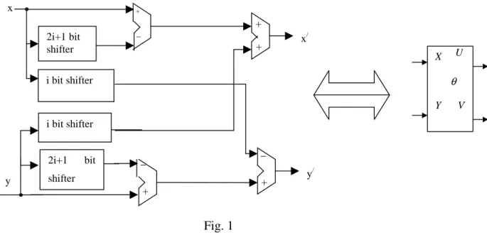
In this paper, the authors first develop a new CORDIC processor, which is scaling
free in nature and the error arising from the approximation of the trigonometric function is analyzed. Subsequently, this processor is used as the basic PE to develop a unified,
asynchronous, wavefront array type architecture for fast computation of DXT - a collective term representing either of the DFT, DHT, DCT or DST. Being multiplierless, the modified CORDIC arithmetic unit is expected to reduce the hardware cost
considerably compared to that of the MAC based designs. Keeping an eye on the low power/low voltage applications, the datapath of the basic PE has been designed and
simulated using TGL in sea of gates semicustom environment. The paper is structured as follows: the theoretical background of the modified CORDIC and the DXT have been developed in Section 2. A brief introduction to the modified CORDIC [9] is also
provided in this section along with its design, layout of the datapath and simulated performance. The proposed array architecture is described in Section 3. In Section 4, the
comparison with five other existing architectures are also described in this section. Conclusions are drawn in Section 5.
2. Theoretical Information:
2.1. The CORDIC unit:
The transforms of DXT family involve trigonometric operations on the input sample
sequences that can be expressed in terms of plane rotations. The CORDIC unit [10] can
iteratively rotate an input vector A = [Ax Ay] through a target angle ψ (say in clockwise
direction) through small steps of elementary angles ψi (so that ∑i ψi = ψ) to generate an
output vector B = [Bx By]. This operation can be represented mathematically as
[Bx By] = [Ax Ay]
cos sin
sin cos
ψ ψ ψ ψ −
(1)
i. e., B = A Rot (ψ) (2)
For fast convergence of the algorithm to the final small angle value, a simple
modification [9] of the conventional CORDIC algorithm is applied here which represents
the small incremental angle by sin ψi≈ψi = 2−i and expresses the basic Rot (ψ) operation
as Rot (ψi) =
1 2 2
2 2 − − − − − − − (2i +1) (2i +1) 1 i
i ; for a 16 bit machine, i ∈ { 4, 5, …., 15}.
(3)
Thus, the rotation through the target angle ψ may be expressed as,
Rot (ψ) =
∏
− = 1 0 b i1 2 2
2 2 − − − − − − − (2i +1) (2i +1) 1 i
i (4)
It is evident from the above formulation that the modified CORDIC unit is free from the scale factor compensation step which saves a significant amount of hardware compared to the conventional CORDIC unit and subsequently makes the CORDIC
operation faster.
Error analysis:
The potential sources of error for the hardware realization of an algorithm are two folds namely, the error due to the quantization of the input word and due to the finite wordlength. In case of CORDIC another potential error source in the error due to
approximation of the target angles. In our scheme, the errors due to first two sources are same as the conventional implementation of the circular CORDIC. Thus, the detailed
analysis of the third error source is presented here with the consideration that the implementation has been done with 16-bit wordlength.
Let θc be the computed angle whereas θ is the ideal target angle. Then from
equation (1),
Bx = Ax cosθc + Ay sinθc (3a)
By = − Ax sinθc + Ay cosθc (3b)
Where θc = θ−ε and ε is the error due to angle approximation. From equation (4) it may
be readily seen that the value of ε is O(2−16). On simplification, equation (3a) and (3b)
yields,
Bxerror = (Ax cosθc + Ay sinθc)(1− cos ε) + (− Ax sinθc + Ay cosθc) sin ε (4a)
Byerror = (− Ax sinθc + Ay cosθc)( 1− cos ε) − (Ax cosθc + Ay sinθc) sin ε (4b)
Since ε = O(2−16), (1− cos ε) and sin ε will be O(2−33) and O(2−16) respectively. Thus the
scheme is O(2−16) which seems to be quite within limit. The simulation result for the
errors due to approximation of different target angles is shown in Figure 2.
To design the low power CORDIC unit, TGL style [11] is used in 1.6 µm double layer
sea of gates semicustom environment.The area of the designed CORDIC chip is (4.4642 x 3.9538) mm2. The performance of the circuit according to the Switch Level timing Simulator (SLS) at 5 V supply is, datapath delay = 54 nsec., power dissipation = 37 mW,
Power-Delay Product (PDP) = 1.998 nJ and Energy-Delay Product (EDP) = 1.078 x 10⁻¹⁶
J-sec. To get the effect of worst case power consumption, the activity factor has been taken as 1. At 5 V supply, the calculated values for delay, dynamic power consumption,
PDP and EDP of the simulated circuit modules used to construct the processor chip are given in Table 1. Layout of one 4-bit conditional sum adder/subtractor is shown in Fig. 2.
These results indicate that this CORDIC processor may be a suitable choice for low power/low voltage operation domain. It is expected that with proper transistor sizing and threshold voltage scaling, the processor will show a better performance and consume less
power [12].
2.2. Theoretical background of the transforms :
Considering a real sample sequence f(n), n ∈{0, 1, ..., N−1} the DXT can be defined
as
DFT : F (k) = f
n N
(n) [cos(2π / N) kn − j sin (2π / N) kn] =
−
∑
0 1
= Fx(k) + j Fy(k) (5)
DHT : H (k) = f(n) [cos(2π / N) kn + sin(2π / N) kn]
n N
= −
∑
0 1
(6)
DCT : C(k) = f(n) cos [ k(2n + 1) / 2N]π
n N
= −
∑
0 1
DST : Z(k) = f(n + 1) sin [ k(2n + 1) / 2N]π n N = −
∑
0 1 (8)In terms of the operator Rot (*), the equations can be represented as
DFT : [ Fx Fy ] = [f(n) 0] Rot (m ) θ n N = −
∑
0 1 (9)DHT : [H(k) H(N−k)] = [f(n) f(n)] Rot (m ) θ
n N = −
∑
0 1 (10)DCT : [C(k) − C(N−k)] = [ [r(n) 0] Rot (m )] Rot (k )
n = 0 N
θ φ
−
∑
1(11)
where k = 0, 1, ..., N − 1; m = kn modulo N (=<kn>N), θ = 2π/N and φ = θ/4 and
r(n) = f(2n) , for n = 0, 1, ..., (N−1)/2
= f(2N − 2n −1), for n = (N + 1)/2, ..., (N−1) (12)
The comparison between equations (7) and (8) shows that DCT and DST are obtainable from either of the two by proper data ordering.
Thus, all of the above four transforms can be clubbed into a single equation as
Y(k) = [ h(n) Rot (m )] Rot (k )θ φ
n N = −
∑
0 1 (13)where m = <kn>N , θ = 2π/N, φ = 0 for DFT/DHT and φ = θ/4 for DCT and DST.
3. Array architecture :
Fig. 3 shows the proposed unified architecture for N = 5. To achieve the operation
Rot(mθ) on the given sample set, the input samples for θ array has been scheduled
according to the permutation sequence of <nk>N (ref. to Table 2). Computation of the
final result has been carried out by rotating the partial results emerging from the θ array
by an angle kφ. The data from the FIFO can be loaded to the registers at the input of the
‘OFF’ states of the mode control switch decide whether the data from the FIFO will go to both the adders or just to one adder. In steady state, the whole operation is summarized in the following pseudocode,
For i = 1 to N, do in parallel /* i = column (for DFT and DHT i varies from 1 to
( N−1)) */
For j = 1 to (N−1), do /* j = row */
Load data (j, i ); /* Load j th data from the i th FIFO to the register of (j, i) th
adder */ For all j, do in parallel
Wait_data (j, i−1); /* Wait until data from the output of (j, i−1) th
processor is available */
Add_data (j, i −1) and (j, i); /* For all j ∈ {1, 2, …, (N−1) } simultaneous addition of
(j, i −1) th and (j, i) th data */
Signal_ start (Processors (j, i)) /* Issue start signal to all j th processor at i th column
when all data from the (j, i) adders are available at the input of i th processor column after addition */ It reveals from Fig. 3 that in order to exploit the inherent pipelinability of the structure,
the clock period Tc of the controlling counter must maintain the relationship, Ad ≤ Tc ≤
Pd / 4, where Ad is the FIFO access time and Pd is the delay of a single processor. The
processed data move through the array like a plane wavefront. However, a suitable
For clarity, using the unified architecture, the computation of 5 point DCT is explained. The data scheduling according to the permutation sequence of <nk>N (ref. to
Table 2) is depicted in Table 3 where U/(k) = U(k) − f(0), the terms U(k)s are the
intermediate results after the rotation in the θ plane. The U(0) term, which is a mere
accumulation (dc term) of the input samples, is omitted in Table 3. The U/(k) terms after
addition with the f(0) terms undergo rotation kφ to generate the complete set of Y(k).
Here the x-component of Y(k) gives rise to the desired DCT of the given sample sequence. The mode control switch is kept in the ‘OFF’ state here to route the data from
the FIFO to the adder at the x inputs of the processors.
Following the same line, the DST can also be obtained by replacing f(n) th sample of
DCT with f(n+1) th sample and considering the y-component of the output vector.
Letting φ = 0, the same architecture is capable to compute DHT and DFT. Data
distribution for the 5 point DHT is shown in Table 4. For computation of DHT, the mode
control switch is kept in the ‘ON’ state. DFT of the sample set can be obtained by inserting f(n) at the x-input of the input vector and putting 0 at the y input. The real and imaginary parts are obtained from the x and y components of the output vector
respectively.
The proposed architecture can be extended for computation of long transform
sequence by simply cascading the modules with lower N. As an example, to compute DCT for N = 11, the architecture for N = 5 is considered as the basic cascading block and coined as generalized module. Table 5 (a) shows the data distribution for 11 point DCT
module. The resulting structure is shown in Fig. 4 where D s are the inputs corresponding to different blocks of data shown in Table 5.
To compute DFT of complex input data sequence, equation (3) may be rewritten as
[Fx (k) Fy (k)] = [f (n) f (n)] Rot (m )x y θ n
N
= −
∑
0 1
(14)
In this case, the operation procedure of the architecture is same as explained earlier, with the difference that fx(n) and fy(n) components (the real and imaginary parts of f(n)) are
stored in a pair of FIFO dedicated for each processor column and they are simultaneously retrieved during operation. The x and y components of the output vector contain the real and imaginary parts of the result respectively.
4. Salient features and comparison with other architectures :
The proposed architecture is compared with five existing architectures and is summarized
in Table 6. The proposed one exhibits local neighborhood connections and is selftimed in nature. Being asynchronous, it is more advantageous than the other systolic designs from fault tolerance perspective. Moreover, the data skewing and subsequent glitch problems
are suppressed considerably. The efficient floor utilization is possible due to its nature of simple interprocessor connections. This architecture exhibits same order of latency as that
of Pan et al. [3] and Mandal et al. [8]. This architecture is inherently a pipelined one and in the steady state its throughput rate is O(N). Thus, the steady state throughput rate has been considerably enhanced than that of other architectures. The area - time complexity
(AT2) of the proposed architecture is O (N4).
Another feature of the proposed architecture is its expandability. The modules calculating
utilization may not be possible for all N. Being cascadable in nature, the proposed architecture is compatible with the WSI (Wafer Scale Integration) technology.
This architecture may be a suitable candidate for low power/low voltage applications.
The architecture is based on modified CORDIC method which implies reduction of power consumption at the algorithmic level since the number of operations have been
reduced. The presence of block level pipelining and parallelism reduce power consumption at the architectural level. The asynchronous operation mode suppresses the glitches and thus a considerable amount of power can be saved. The CORDIC is designed
using TGL and thus reduction of circuit level power consumption is achieved. Therefore, the proposed architecture can save power in the algorithm, architecture and circuit level.
6. Conclusions :
The proposed architecture is an asynchronous, wavefront array type capable of computing DXT. Being data driven and self timed in nature, it eliminates the data
skewing and subsequent glitch problems. However, a suitable handshaking protocol is to be adopted to maintain the data driven property. The advantage of modified CORDIC PE
stems from an expected lower area consumption than the MAC based PE. Use of
CORDIC eliminates the requirement of precomputation of cosθ and sinθ. The simple
local interprocessor connection leads to the efficient utilization of the floor space and subsequent reduction in routing area. The presence of inherent pipelining and
concurrency in this architecture are advantageous so far the low power/low voltage operation is concerned. Construction of the CORDIC module using TGL methodology
A comparative study of the proposed architecture with five other existing architectures reveals its superiority in speed (in terms of latency and throughput) and in processor interconnection over the others. It does not require any global timing synchronization or
complicated data manipulations and can straightway be cascaded to realize longer transformation sequences and thus is WSI compatible. The same architectural
methodology can be adopted for multidimensional DXT computation and for non prime transform length also.
REFERENCES
[1] A. K. Jain, Fundamentals of Digital Image Processing, Prentice Hall, Englewood
Cliffs, 1989.
[2] A. M. Tekalp, Digital Video Processing, Prentice Hall PTR, Upper Saddle river, NJ, 1995.
[3] Sung Bum Pan and Rae-Hong Park, “Unified systolic arrays for computation of DCT/DST/DHT”, IEEE Trans. Circuits Syst. Video Tech., vol. 7, no. 2, pp. 413 - 419,
Apr. 1997.
[4] N. I. Cho and S. U. Lee, “DCT algorithms for VLSI parallel implementations”, IEEE
Trans. Acoust., Speech, Signal Processing, vol. 38, pp. 121 - 127, Jan. 1990.
[5] L. W. Chang and M. C. Wu, “A unified systolic array for discrete cosine and sine transforms”, IEEE Trans. Signal Processing, vol. 39, pp. 192 - 194, Jan. 1991.
[7] C. Chakrabarti and J. JaJa, “Systolic architectures for the computation of the discrete Hartley and the discrete cosine transforms based on prime factor decomposition”, IEEE
Trans. Comput., vol. 39, pp. 1359 - 1368, Nov. 1990.
[8] M. C. Mandal et al., “Multiplierless array architecture for computing discrete cosine transform”, Computers Elect. Engng., vol. 21, no. 1, pp. 13 - 19, 1995.
[9] A. S. Dhar and S. Banerjee, “An array architecture for fast computation of discrete Hartley transform”, IEEE Trans. Circuits Syst., vol. 38, no. 9, pp. 1095 - 1098, 1991. [10] G. Haviland and A. Tuzynski, “A CORDIC arithmetic processor chip”, IEEE Trans.
Comput., vol. C29, pp. 68 - 79, 1980.
[11] K. Maharatna et al., “A 52 MHz 1.5 V 16 bit high performance shifter circuit”, in
Proc. 5 th International Conference on VLSI and CAD, Seoul, Korea, pp. 478 - 480, Oct.
1997.
[12] A. Bellaouar and M. I. Elmasry, Low-Power Digital VLSI Design, Circuits and
Systems, Kluwer Academic Publishers, 1995.
[13] R. N. Bracewell, “The fast Hartley transform”, Proc. IEEE, vol. 72, pp. 1010 - 1018,
Aug. 1984.
Cell name Delay
(nsec)
Power (mW) @ 18.5 MHz
PDP (pJ) EDP (J-sec)
Multiplexer bank 0.07 1.2536 0.0877 6.1426 X 10 -24
16 bit register 0.7 3.0889 2.1622 1.5135 X 10 -21
Shifter 19 0.8289 15.7493 2.9923 X 10 -19
Adder/Subtractor 7.1 4.0538 28.7823 2.0435 X 10 -19
1 2 3 4
1 1 2 3 4
2 2 4 1 3
3 3 1 4 2
4 4 3 2 1
Table 2
n k
1θ 2θ 3θ 4θ U’(1) f(2) f(4) f(3) f(1) U’(2) f(3) f(2) f(1) f(4) U’(3) f(4) f(1) f(2) f(3) U’(4) f(1) f(3) f(4) f(2)
1θ 2θ 3θ 4θ Y’(1) f(1) f(2) f(3) f(4) Y’(2) f(3) f(1) f(4) f(2) Y’(3) f(2) f(4) f(1) f(3) Y’(4) f(4) f(3) f(2) f(1)
1θ 2θ 3θ 4θ 5θ 6θ 7θ 8θ 9θ 10θ Y’(1) f(2) f(4) f(6) f(8) f(10) f(9) f(7) f(5) f(3) f(1) Y’(2) f(9) f(2) f(7) f(4) f(5) f(6) f(3) f(8) f(1) f(10) Y’(3) f(8) f(5) f(2) f(10) f(3) f(4) f(9) f(1) f(6) f(7) Y’(4) f(6) f(9) f(3) f(2) f(8) f(7) f(1) f(4) f(10) f(5) Y’(5) f(3) f(7) f(10) f(6) f(2) f(1) f(5) f(9) f(8) f(4) Y’(6) f(4) f(8) f(9) f(5) f(1) f(2) f(6) f(10) f(7) f(3) Y’(7) f(5) f(10) f(4) f(1) f(7) f(8) f(2) f(3) f(9) f(6) Y’(8) f(7) f(6) f(1) f(9) f(4) f(3) f(10) f(2) f(5) f(8) Y’(9) f(10) f(1) f(8) f(3) f(6) f(5) f(4) f(7) f(2) f(9) Y’(10) f(1) f(3) f(5) f(7) f(9) f(10) f(8) f(6) f(4) f(2)
Y’(1)
Y’(2) D11 D12 D13 Y’(3)
Y’(4) Y’(5)
Y’(6) D21 D22 D23 Y’(7)
Y’(8)
Y’(9) D31 D32 D33 Y’(10)
Cho & Lee [4]
Chang & Wu [5]
Lee [6] Pan [3] Mandal [8] Proposed
Nature of architecture
Systolic Systolic Systolic Systolic Systolic Wavefront
Table 3
Table 4
Nature of operation
Sequential sequential sequential sequential concurrent concurrent
Number of operational blocks
4
multipliers
2 multipliers 8 multipliers 2 multipliers multiplierless CORDIC (4 adders and 4 shifters)
multiplierless CORDIC (4 adders and 4 shifters)
Number of PE
N + 1 N + 1 N –1 N/2 N x (N - 1) N x (N - 1)
Total number of multipliers
4 (N +1) 2 (N – 1) 8 N N no requirement
of real
multiplication operation
no requirement of real
multiplication operation Latency O(2N) O (2N - 2) O[2(√N+1) +
√N+2]
O (N) O (N) O (N)
Throughput O(1) O(1) O(1) O(1) O(1) O(N)
Fig. 1
+
+ y
_ +
_
y/ x/ x
2i+1 bit shifter
2i+1 bit shifter i bit shifter
X
Y U
V
θ i bit shifter
_
+
O/P From FIFO
I/P
FIFO Bank
θ
θ
θ
θ
θ
θ
θ
θ
θ
θ
θ
θ
θ
θ
θ
θ
φ
2φ
3φ
4φ
SWITCH ARRAY AND CONTROL COUNTER
0
0
0 0
GMc
Fig. 3
θ θ MODE CONT
X
Y U
V
X
Y U
V
θ θ
f
GMC
D33 GMC GMC
unused Y(10) Y(9)
Fig. 4
Y(4) Y(3) Y(2) Y(1) D12
D23
0 0
GMC
D13
GMC
0
GMC
D33
D22
GMC
GMC
D32
GMC
D11
D21
GMC
GMC
D31
GMC
Y(8) Y(7) Y(6) Y(5)
unused Y(10) Y(9)
Fig. caption
Fig. 1. The block diagram of the modified CORDIC unit. Fig. 2. Layout of 4 bit adder/subtractor (conditional sum type). Fig. 3. The architecture for N = 5 and the symbol (GMC).
Fig. 4. The cascaded architecture for 11 point DCT using 5 point DCT modules as the basic block.
Table caption
Table 1. Power performance of different blocks used to construct the CORDIC unit. Table 2. The permutation table of nk modulo N for N = 5.
Table 3. The data scheduling for 5 point DCT derived from Table 1.
Table 4. The data scheduling for 5 point DHT derived from Table 1.
Table 5. The data scheduling for 11 point DCT and its representation in the form of
block data (D*).