Microstructural Analysis of CdTe Radiation Detectors with Indium Electrodes
Miki Moriyama
1, Masahiro Kunisu
2;*1, Atsushi Kiyamu
3, Ryoich Ohno
3and Masanori Murakami
2;*21Optoelectronics Division, Toyoda Gosei Co., Ltd., Heiwa-cho, Nakashima, Aichi 490-1312, Japan 2Department of Materials Science and Engineering, Kyoto University, Kyoto 606-8501, Japan 3
ACRORAD, Gushikawa, Okinawa 904-2234, Japan
In order to understand the formation mechanisms of indium contacts which were previously developed for CdTe radiation detectors with p–i–n structure, microstructure of the indium contacts which were deposited at various substrate temperatures on the p-CdTe substrates and subsequently annealed at temperature ranging from 200 to 400C were analyzed by X-ray diffraction and transmission electron microscopy. The
microstructural analysis revealed that reactions between CdTe and In were enhanced by the substrate heating during deposition and growth of In4Te3or InTe compounds on the CdTe surface was observed. Current leakage and stability of the CdTe radiation detectors were strongly
correlated with the microstructure of CdTe/contact interfaces. The indium contacts, which were deposited at substrate temperature of 400 or 350C and subsequently annealed at 350C for 1 h in vacuum, displayed rectifying I–V behaviors and satisfied the device requirement. In
addition, the excellent thermal stability of these contacts was observed. We found that the formation of the InTe compounds was essential for production of the p–i–n CdTe detector devices which require highly reliable rectifying contacts.
(Received April 27, 2005; Accepted June 17, 2005; Published September 15, 2005)
Keywords: p–i–n diode, radiation detectors, cadmium telluride, heterojunction, indium telluride
1. Introduction
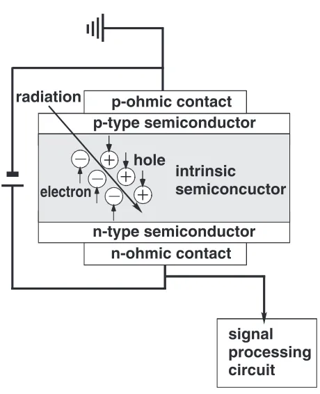
Detection accuracy and stability of a semiconductor radiation detector is strongly influenced by the device structure.1)An ideal structure for high-resolution X-ray and gamma-ray radiation detectors is to have p-type semicon-ductor/intrinsic/n-type semiconductor which is convention-ally called as p–i–n diode. Figure 1 shows a schematic drawing of the p–i–n diode detector. The detector consists of a single crystal having an intrinsic or lightly doped semi-conductor sandwiched by p- and n-type semisemi-conductors. A reverse-bias voltage applied across the detector depletes charge carriers in the intrinsic semiconductor, constituting the radiation sensitive volume. When the incident radiation interacts the depleted semiconductor region, electron-hole pairs proportional to the energy and amounts of the incident radiation are generated. The applied electric field separates these carriers to the respective contacts, leading to a current flow in the external circuit as the carriers drift across the depletion layer. The high resolution detectors must collect all charged carriers to the respective contacts.
Requirements for the intrinsic semiconductor are as follows.
(1) Since the dark leakage current induces an electric noise, a semiconductor with low leakage current at a high electric field is required. Thus, a bandgap energy (Eg) of the semiconductor should be large.
(2) For high quantum efficiency for photons, a semi-conductor with strong radiation absorption at a rela-tively thin (<1mm) intrinsic layer is required. Thus, an average atomic number of the semiconductor should be high.
Cadmium telluride (CdTe), which has a large energy bandgap (1:5eV) and a high average atomic number
(ZCdTe ¼50), satisfies these requirements, and operates at room temperature with high energy resolution.2) Excellent performances of the CdTe detectors with p–i–n structure were experimentally demonstrated by many researchers.3–6) Shin et al. fabricated p–i–n detectors by sandwitching the CdTe substrate with p-type and n-type heteroepitaxial HgCdTe layers.6) Niraula et al. grew an iodine doped n-CdTe layer on the Te-face of n-CdTe by a metalorganic chemical vapor deposition (MOCVD) technique.5)However, the CdTe detectors deteriorated when the CdTe crystals were exposed to a high temperature during the junction fabrication process. In addition, the long-term stability during detector
radiation
p-type semiconductor
hole
electron
n-type semiconductor
intrinsic
semiconcuctor
p-ohmic contact
n-ohmic contact
signal
processing
circuit
+
+
+
Fig. 1 Schematic drawing of a p–i–n diode detector.
*1Graduate Student, Kyoto University
*2Corresponding author,
E-mail: [email protected] Special Issue on Narrow and Wide-Bandgap Semiconductor Materials
[image:1.595.312.542.328.611.2]operation was the key issue for a practical use of the p–i–n CdTe detector. Degradation of the detection performance during device operation (called as a polarizaion effect) was often observed in the detector with p–i–n structure.7) Although the detection performance recovered after the bias was re-applied, the polarization effect did not satisfy the stability requirement of the practical use. Therefore, it was necessary to develop a simple, low temperature fabrication process for the CdTe detector with high stability.
Recently, a significant improvement in the spectral properties and the stability of the CdTe detectors using homogeneous CdTe crystal was achieved by Ohnoet al.8–12)
They prepared a rectifying In contact on the Te-terminated surface of the CdTe semiconductor with low hole concen-tration by depositing In on the substrate kept at high temperature, and a Pt contact on the Cd-terminated surface of the CdTe semiconductor as ohmic contact by electroless plating.12)Since the barrier height at the Pt/p-CdTe interface is relatively low, these detectors would have p–i–n diode structure, where a n-type semiconductor might be formed at the interface between the In contact and the p-CdTe semiconductor.
The purpose of the present study is to investigate an intermediate semiconductor formed at the interface between the In contact and the CdTe by analyzing the interfacial microstructure using X-ray diffraction (XRD) and trans-mission electron microscopy (TEM). These studies will provide us a guideline for developing the electrodes used in the high performance CdTe radiation detectors.
2. Experimental Procedures
The Te or Cd terminated (111) oriented CdTe single crystals were grown by a traveling heat method (THM-CdTe),13)where Cl atoms were doped at a level of 2 ppm. The typical electrical resistivity of the CdTe crystals was about 1{2109cm and the Hall measurements indicated the
CdTe crystals had p-type conduction. Prior to contact metal deposition, the CdTe substrate surfaces were chemically cleaned by immersing in 1% Br-methanol solution for 2 min at room temperature. The In electrodes were deposited at the rate of 3 nm/sec on the CdTe substrates which were kept at various temperatures as listed in Table 1. Samples A’s were prepared by depositing In on the CdTe substrates which were cooled at liquid nitrogen temperature during depositions since it was difficult to prepare an uniform thin In layer at
room temperature. Samples B’s, C’s, and D were prepared by the following steps. First, the substrates were loaded into a vacuum chamber with the base pressure of below 2106Pa, and were isothermally annealed at a
temper-ature ranging from 200 to 400C for 30–60 min in the
vacuum chamber. Then, indium (In) layers with thickness of 300 nm were evaporated on the CdTe substrates with Te-terminated surface which were kept at a predetermined temperature for about 20 min.
Some of the CdTe/In samples were subsequently post-annealed in a vacuum at a temperature in the range of 200 to 400C. After the In deposition, Pt layers were plated on the
opposite (Cd-terminated surface) of the CdTe wafer by electroless plating. These Pt contacts showed ohmic I–V behavior.
The leakage current was measured at room temperature in a dark room and the performance of the radiation detectors were evaluated using various radiation sources in Acrorad.14) The surface morphology of the samples was observed by an optical microscope. Microstructural analyses were carried out for the samples before and after annealing using X-ray diffraction (XRD), a focused ion beam system (FIB), and cross-sectional transmission electron microscopy (XTEM).
3. Experimental Results
Interfacial microstructures of the In contacts prepared on the p-CdTe substrates by the various methods (Table 1) were analyzed. Figures 2(a) and 2(b) show the optical microscope images of Sample-A1 and A2, respectively. The In layer surface of Sample-A1 is very smooth. However, the In layer balls up upon annealing at 200C as seen in Fig. 2(b). It is
interesting to note that the each island shown in Fig. 2(b) has a doughnut shape although the reason is not clear at the moment. The XRD measurements (the data are not shown here) showed that reaction between CdTe and In was negligibly small even after the annealing at 200C although
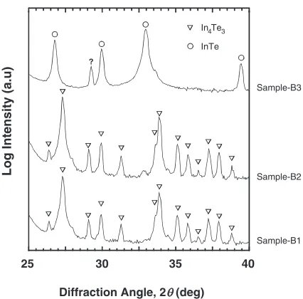
this temperature is higher than the melting point of indium. The interfacial reactions between the CdTe and the In layers of Samples B’s were observed by XRD analysis, and the X-ray profiles are shown in Fig. 3. For Sample-B1, no diffraction peaks from In are detected and several peaks corresponding to In4Te3 (indicated by open triangles) are
observed. (The excess Cd would be evaporated at the high temperature or dispersed at the grain boundaries) The present result indicates that reaction between In and CdTe was enhanced by heating the substrate during In depositions. Since X-ray profiles of Sample-B1 and B2 are similar, the In4Te3compounds are thermally stable at 200C. However,
as seen in X-ray profile of Sample-B3 after annealing at 400C for 2 h, new peaks (indicated by open circles) are
detected at2¼26:8, 30.0, 33.0, and 39.5. These peaks
correspond to [211], [220], [202], and [222] peaks of tetragonal InTe compounds, respectively. The results indi-cate that In4Te3compounds are unstable and reacts with the
CdTe to the InTe compounds at a temperature close to 400C.
(The excess Cd would also evaporate or dispersed at the grain boundaties.)
[image:2.595.47.293.652.765.2]The XRD profiles of C1, C2, and Sample-D1 are shown in Fig. 4. For Sample-C1, diffraction peaks
Table 1 Samples used in the present experiment.
Samples Substrate temperature Annealing condition Sample-A1 Liquid Nitrogen —
Sample-A2 Liquid Nitrogen 200C for 2 h
Sample-B1 200C —
Sample-B2 200C 200C for 0.5
Sample-B3 200C 400C for 2 h
Sample-C1 350C —
Sample-C2 350C 350C for 1 h
Sample-D1 400C —
: prepared in Kyoto Univ.: prepared in ACRORAD: deposited in
corresponding to the In4Te3compounds are observed. These
compounds are transformed to the InTe compounds after annealing at 350C for 1 h as seen in the X-ray profile of
Sample-C2. For Sample-D1, peaks corresponding to InTe are detected immediately after the In deposition. These results indicate that the In4Te3 compounds are thermodynamically
metastable at 350C.
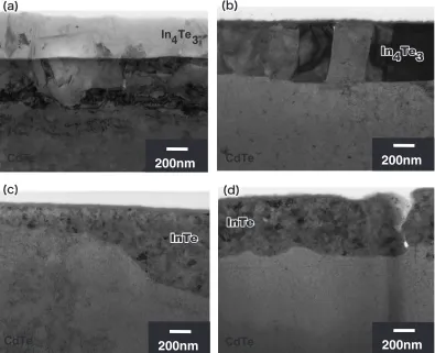
Figures 5(a)–(d) are cross-sectional TEM images of Sample-B1, C1, C2, and D1, respectively. In Sample-B1(a) or C1(b), large polycrystalline In4Te3grains were observed.
The average grain size of the In4Te3grains is measured to be
approximately 200 nm, and the reaction depth of the In4Te3
grains into the CdTe substrate is about 300 nm. Most grains grow epitaxially on the CdTe substrate and the interface between the In4Te3 grains and the CdTe surface is smooth.
When In is deposited on the CdTe substrate at 400C, the reaction layer has small grains with the size of about 50 nm and most grains have random crystal orientations as shown in Fig. 5(c). Such small grained layer is observed when the samples with large In4Te3 grained layer was annealed at
350C for 1 h [Fig. 5(d)]. Note that the interfaces between
InTe and CdTe are very rough.
4. Discussion
4.1 Possibility of formation of p–i–n structure diode by high temperature In deposition
The electrical properties of the In contacts deposited on p-type CdTe at elevated temperatures and the radiation detection performances of the Pt/CdTe/In detectors were studied by Ohno and the details were given elsewhere.14) Ohno found that the In deposition on the CdTe substrates which were kept at high temperature reduced significantly the leakage current and that the high substrate temperature deposition was desirable for production of the stable detectors. Correlation between the detection performance14) and the CdTe/In interfacial microstructure analysed in the present experiment is summarized in Table 2. The XRD and XTEM observations reveal that the leakage current and the thermal stability of the CdTe radiation detectors are strongly correlated with the microstructure of the CdTe/contact interfaces.
4.2 Effects of p-CdTe/InTe compound interface on the electrical properties
The CdTe/In interfacial microstructures prepared by
25 30 35 40
Diffraction Angle, 2 (deg)
Log Intensity (a.u)
θθ
Sample-B1 Sample-B2 Sample-B3 ?
In4Te3
InTe
Fig. 3 XRD profiles of Sample-B1, Sample-B2, and Sample-B3.
Fig. 4 XRD profiles of Sample-C1, Sample-C2, and Sample-D3.
10
µµ
m
10
µ
m
(a)
(b)
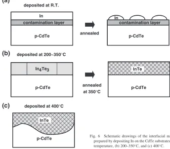
[image:3.595.318.535.69.279.2] [image:3.595.50.290.71.397.2] [image:3.595.63.276.451.661.2]depositing at various substrate temperatures are schemati-cally illustrated in Figs. 6(a)–(c). Microstructural analysis of the present study revealed that the In4Te3or InTe compounds
[image:4.595.101.496.74.395.2] [image:4.595.47.290.467.532.2]were grown on the CdTe surface when In were deposited at elevated temperatures [Figs. 6(b) and (c)]. On the other hand, the interfacial reactions were not detected in the samples which were prepared by depositing at relatively low temper-atures and subsequent annealing at elevated tempertemper-atures [Fig. 6(a)]. It is well known that the surface properties of the substrates play a key role in reaction at the substrate/metal interfaces. The surface properties of CdTe prepared by various surface treatments were extensively investigated by other authors.15) In chemically etched samples, thin oxide (TeOx) layers or amorphous contaminated layers were observed to grow on the CdTe surface [Fig. 6(a)]. The fact that the reactions between CdTe and In were enhanced by heating the substrate during depositions indicated that the surface oxides or the contaminants were cleaned by the substrate heating in vacuum [Fig. 6(b)].
The present experimental results clearly indicated that the formation of indium telluride compounds would play an important role in the electrical properties at the CdTe/contact interfaces and the detector stability. Especially, the detector stability of the CdTe/InTe structure was significantly improved. Based on both the present microstructural analysis and the electrical properties, a current transport mechanism of the In-based contacts for p-CdTe are discussed below.
It was reported that the tetragonal InTe compound has the metallic electrical properties as well as semiconducting properties.16)Jansen and Moodera demonstrated that hetero-junctions which were formed by evaporating the crystalline InTe films onto the p-type Si substrates displayed rectifying I–V behavior with low reverse-bias leakage current.17)These results suggested that the In contacts deposited at the elevated temperatures formed the InTe compound layers with n-type semiconductor property and the p/n junction was formed on the p-type CdTe substrate. This is a reason why the leakage currents were drastically decreased in the CdTe/InTe structures. Although there are a few reports for the conduction type of the In4Te3 compound, we believe that
the In4Te3compound is also n-type semiconductor and forms
heterojunction on p-CdTe.
The polarization effect can be explained by a non-uniform electric field due to the charge accumulation at the metal/ semiconductor interface, although the detailed mechanism for the polarization effect is not fully understood at the moment. The polarization effect appears when the internal electric field by the accumulated charge becomes comparable
200nm
200nm
CdTe
200nm
200nm
CdTeCdTe
In 4Te3
CdTe
Fig. 5 Cross-sectional TEM images of (a) Sample-B1, (b) Sample-C1, (c) Sample-D1, and (d) Sample-C2.
Table 2 Correlation between the CdTe/In interfacial microstructures and the electrical stability.
Sample Contact materials Electrical Stability Sample-B1 In4Te3 poor (a few min.)
Sample-C1 In4Te3 good (30min.)
to the electric field generated by the external bias, causing reduction of a depletion layer thickness in the intrinsic semiconductor. In order to increase the quantum efficiency, the depletion layer must be sufficiently thick to absorb large amounts of the incident radiation. Thus, the effect could be minimized by operating the detectors under a high applied electrical field for which a depletion layer becomes thicker than a thickness of CdTe. In the present experiment, we believed that the InTe contacts deposited at elevated substrate temperatures are essential for production of stable CdTe radiation detectors with high energy resolution.
5. Summary
The interfacial microstructure and the electrical properties of the indium contacts which were prepared by depositing at various substrate temperatures on the p-CdTe substrates and subsequently annealing at temperatures between 200 and 400C were investigated. The XRD and XTEM observations
revealed that the substrate heating during the In deposition facilitated the reaction at the CdTe/In interfaces to form the In4Te3 or InTe compounds. The leakage current and the
stability of the CdTe radiation detectors were strongly correlated with the microstructure of CdTe/contact inter-faces. The formation of the InTe compounds with n-type conduction are concluded to be essential for the production of the highly reliable CdTe radiation detectors with p–i–n structure.
Acknowledgement
This work was partially supported by the Grand-in-Aid for
Scientific Research in the Ministry of Education, Science and Culture of Japan (No. 13450287).
REFERENCES
1) S. Ricq, F. Glasser and M. Garcin: Nucl. Instrum. Methods Phys. Res. A442(2000) 45–52.
2) P. Siffert: Mat. Res. Soc. Symp. Proc.19(1983) 87.
3) R. Sudharasanan, G. D. Vakerlis and N. H. Karam: J.E.M.26(1997) 745.
4) A. Khusainov: Nucl. Instrum. Methods Phys. Res. A322(1992) 335– 340.
5) M. Niraula, D. Mochizuki, T. Aoki, Y. Hatanaka, Y. Tomita and T. Nihashi: Appl. Phys. Lett.75(1999) 2322–2324.
6) S. H. Shin, G. T. Nizawa, J. G. Pasko, G. L. Bostrup, F. J. Ryan, M. Khoshnevisan, C. I. Westmark and C. Fuller: IEEE Trans. Nucl. Sci. NS-32(1985) 487.
7) H. L. Malm and M. Martini: IEEE Trans. Nucl. Sci. NS-21(1974) 322. 8) M. Funakiet al.: Nucl. Instr. Meth. A436(1999) 120.
9) T. Takahashi, K. Hirose, C. Matsumoto, K. Takizawa, R. Ohno, T. Ozaki, K. Mori and Y. Tomita: SPIE3446(1998) 29.
10) T. Takahashi and S. Watanabe: IEEE Trans. Nucl. Sci.48(2001) 950– 959.
11) M. Moriyama, M. Murakami, A. Kiyamu and R. Ohno: Japanese Patent, No. 2002-344000.
12) T. Ozaki, Y. Iwase, H. Takamura and M. Ohmori: Nucl. Instrum. Methods Phys. Res. A380(1996) 141–144.
13) M. Ohmori, Y. Iwase and R. Ohno: Mater. Sci. Eng. B16(1999) 283– 283.
14) Development of new semiconductor radiation detectors for medical diagnosis, Report of Regional Consortium Project of NEDO, No. 010018524 (2000).
15) J. P. Ponpon: Solid-State Electron.28(1985) 689–706. 16) Semiconductors Basic Data, (Springer 1996).
17) R. Jansen and J. S. Moodera: Appl. Phys. Lett.75(1999) 2100–2102.
p-CdTe contamination layer
In deposited at R.T.
p-CdTe contamination layer In
annealed
p-CdTe deposited at 200~350°C
In4Te3
annealed at 350°C
p-CdTe deposited at 400°C
(a)
(b)
(c)
p-CdTe InTe
InTe
[image:5.595.123.467.81.383.2]