Atomically resolved STM imaging with a diamond tip:
simulation and experiment
V. Grushko
1*, O. Lübben
2, A. N. Chaika
2,3**, N. Novikov
1, E. Mitskevich
1,
A. Chepugov
1, O. Lysenko
1, B. E. Murphy
2, S. A. Krasnikov
2, I. V. Shvets
21
V. Bakul Institute for Superhard Materials, Kiev, 04074, Ukraine
2
Centre for Research on Adaptive Nanostructures and Nanodevices, School of Physics, Trinity
College, Dublin 2, Ireland
3
Institute of Solid State Physics RAS, Chernogolovka, Moscow district 142432, Russia
*e-mail:
; **e-mail:
,
,
I. Introduction
The scanning tunneling microscope (STM) is one of the most powerful surface science tools for the imaging, characterization, and fabrication of atomic structures. It is well known that the electronic structure of the tip apex atom plays a key role in STM tunneling [1-3]. Particularly, for some tip-sample systems an agreement between experiment and simulation could only be obtained by including the fine tip electronic structure in calculations [4-9]. It is known that the electronic structure of a realistic tip is usually determined by a mixture of s-, p- and d -states while the local density of -states (LDOS) near the Fermi level can be highly dependent on the energy of tunneling electrons [3]. However, theoretical approaches routinely applied to describe the tunneling (e.g., Tersoff-Hamann approximation [4]) use the models without considering the contribution of the tip electron states with non-zero angular momentum projections on the quantization axes which can dominate at small tip-sample distances [2, 10-12]. The most sophisticated theoretical methods are based on the scattering approach and, generally, the Lippmann-Schwinger (LS) equation [13], while the assumption of a weak interaction between the STM tip and the sample is the
basis for a perturbation approach which leads to the formulation of Bardeen [14]. Extensive studies are currently being undertaken to develop non-perturbative methods to calculate the tunneling current in the quantum-mechanical "STM tip – sample surface" system. However, non-perturbative calculations generally demand a lot of time and powerful computational resources. Therefore, in most cases the tip-sample interaction is treated either by a perturbation approach [15] or by non-perturbative methods using simple potentials [16, 17].
It has been demonstrated in a number of recent studies that extremely small (2–3 Å) tunneling distances [18-22] are often required to achieve the ultimate resolution in STM experiments. At such small distances, the perturbation approach generally fails because of the strong interaction between the tip and surface atoms. Therefore the non-perturbative approach is required to find the dependence of the tunneling current from the tip-surface distance. It has also been demonstrated recently that the orbital structure of a metallic probe can induce unusual electronic effects on a subatomic scale [8, 9, 18-20], which can complicate the explanation of experimental atomically resolved images. For this reason light element-terminated probes with spatially localized atomic orbitals at the apex which have a
minimal number of electron states involved in the tunneling can provide enhanced spatial resolution in STM experiments [21, 22] and simplify the interpretation of atomically resolved STM data. However, the methods proposed for the fabrication of light atom terminated probes so far [21-23] could not routinely produce stable tips with a controlled atomic and electronic structure at the apexes. In this manuscript we show that oriented boron-doped single crystal diamond tips can be considered as very promising probes for high-resolution STM studies. In our previous studies [24, 25], we have shown that the unique stability of semiconducting diamond tips allows for successful surface studies on the nanoscale under ambient conditions. The stability of the tip apex is crucial for ultrahigh vacuum (UHV) studies with atomic resolution. For a detailed understanding of the tunneling parameters optimal for high resolution imaging with diamond probes, we analyze in this work the interaction between the <111>-oriented diamond tip and the graphite surface and its influence on the tunneling current and electronic structure of the tip and surface atoms. We have calculated the partial density of electron states (PDOS) of the interacting atoms and the contribution of different atomic orbitals of the diamond tip apex atom using density functional theory (DFT) and the non-perturbative approach proposed in [26], respectively. Our STM experiments and theoretical calculations demonstrate that high vertical and lateral resolution can be achieved with conductive diamond probes both at relatively large tunneling gaps, when the pz-orbital of the tip provides the maximum contribution to the tunneling current, and small gaps when the noise in the tunneling current is very high due to increased tip and sample atom interactions. The DFT and current calculations have allowed us to define the best parameters for atomically resolved imaging with diamond probes and estimate the maximal errors in the tunneling current measurements that still permit atomically resolved STM studies.
II. Preparation of diamond probes for STM experiments
A p-type boron-doped IIb diamond single crystal synthesized by the temperature gradient method under high pressure–high temperature (HPHT) conditions was used as a material for the STM tips. Procedures for the growth of diamond crystals with controlled physical properties, selection of the synthesized crystals with the desired habitus and their precise shaping in the form of pyramid have been described recently [24]. The boron-doped single crystal diamond probes with properly shaped pyramids at the apex (Fig. 1) were mounted onto the STM tip holder and rinsed in ethanol prior to loading into the UHV chamber of a room temperature STM. The base pressure in the STM GPI-300 chamber was kept below 1×10⁻¹⁰ mbar. The diamond probes were
cleaned by Ar+-sputtering with the ion beam (E
i=600 eV) directed along the tip axis (the <111> direction
of the diamond crystal lattice). The pressure in the UHV chamber during the ion sputtering was kept in the range of 3–5×10⁻⁵ mbar. Typically, after
continuous (30-120 min.) co-axial ion sputtering the diamond tip apex was suitable for atomically resolved STM studies on a graphite (0001) surface.
III. Results and discussion
III. 1. STM experiments with a diamond tip on a graphite surface
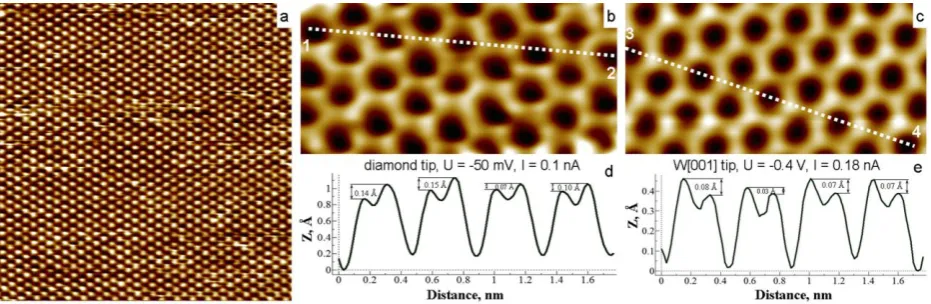
[image:2.595.320.544.56.230.2]tungsten tip used for orbital-resolved experiments [19, 20]. Note that in those studies, the individual d -electron orbitals of the tungsten tip atom were imaged with sub-Ångström lateral resolution using the carbon orbitals of the surface atoms. The image measured with the W[001] tip [Fig. 2(c)] also reveals two non-equivalent surface atoms in the honeycomb lattice but hollow sites are not as deep (see cross-sections on Figs. 2(d) and 2(e)) and individual surface atoms are not as well resolved when compared to the image obtained with the boron-doped diamond probe shown in Fig. 2(b).
Figure 3 demonstrates that both types of atomically resolved images of the graphite surface can be obtained with an unchanged single crystal diamond tip at different gap resistances. Although the sequence of images in Fig. 3 does not provide the highest quality patterns measured during our experiments (Figs. 2(a) and 2(b)), it illustrates that the honeycomb pattern can typically be resolved at larger tip-sample distances, characterized by a smaller tip and surface atom interaction (Figs. 3(a) and 3(f)). This fact suggests that the different depths of the hollow sites on images resolved with the single crystal diamond and tungsten probes can be related to the fundamentally different orbital structure of the two tips. The gap resistance dependence in Fig. 3 demonstrates the reproducible contrast inversion from honeycomb to the hexagonal pattern at decreasing gap resistances (tip-sample separations), which is in agreement with earlier distance-dependent
studies carried out with W[001] tips [19] and theoretical calculations, [27] suggesting a transition between imaging the surface carbon atoms to imaging the hollow sites due to multiple scattering effects at small tunneling gaps.
III.2. DFT calculations of the PDOS of interacting tip and surface atoms
DFT calculations were performed using the Vienna
Ab-initio Simulation Package (VASP) program. VASP implements a projected augmented waves basis set and periodic boundary conditions [28]. The electron exchange and correlation was simulated by local density approximation (LDA) pseudopotentials with a Ceperley-Alder exchange-correlation density functional [29]. A Gamma-centered (1×1×1) k-point grid was used for all calculations to sample the Brilliouin zone. For the DOS a smearing of 0.2 eV was applied using the Methfessel-Paxton method. The global break condition for the electronic self-consistent loops was set to a total energy change of less than 1×10⁻⁶ eV.
[image:3.595.73.539.57.209.2]The simulated graphite (0001) surface consisted of six unit layer slabs (300 atoms). To model the diamond tip, a pyramid in the [111] orientation was modeled out of two unit layer slabs plus an additional six unit layer labs to account for the bulk (320 atoms in total). Tip–sample separations from 1.5 Å up to 4.5 Å were applied to calculate the tip and surface atom PDOS dependence on the tip- Figure 2. 81 Å × 81 Å (a) and 18 Å × 9 Å (b) atomically resolved STM images of the graphite (0001) surface measured with diamond probes at U = -0.2 V and It= 0.14 nA (a) and U = -50 mV and It= 0.1 nA (b). (c) An 18 Å × 9 Å STM image of the
graphite surface measured with a [001]-oriented single crystalline W probe at U = -0.4 V and It= 0.18 nA. The images in
panels (b) and (c) were smoothed by 3×3 matrix [38] while panel (a) represents a raw image without filtering or smoothing applied. (d,e) Cross-sections 1-2 (d) and 3-4 (e) of the images in panels (b) and (c) illustrating the non-equivalence of the surface α and β atoms and the high spatial resolution which can be achieved using single crystalline diamond probes.
Figure 3. 8.5 Å × 8.5 Å constant current STM images of the graphite (0001) surface measured successively (from (a) to (f)) with an unchanged single crystalline diamond probe at different gap resistances. The images were taken at U = -0.4 V and It =
0.2 nA (a), U = -0.1 V and It = 0.08 nA (b), U = -0.1 V and It = 0.3 nA (c), U = -0.1 V and It = 0.5 nA (d), U = -0.1 V and It =
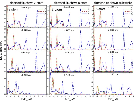
[image:3.595.71.540.288.366.2]Figure 4. PDOS of the diamond tip atom at different tip-sample distances and lateral positions of the tip. The tip-sample distances are indicated on each particular frame.
[image:4.595.84.535.431.773.2]surface distance. The spacing between the back of the tip slab and the HOPG was ~ 17 Å for a distance of 4.5 Å, for all other distances it was correspondingly larger.
Figures 4 and 5 show the dependence of the tip and surface atoms’ PDOS on the tip-surface separation, respectively. The PDOS was calculated for three lateral positions of the diamond tip over the graphite surface, namely, above the α and β atoms and the hollow site.
III.3. Calculations of the tunneling current
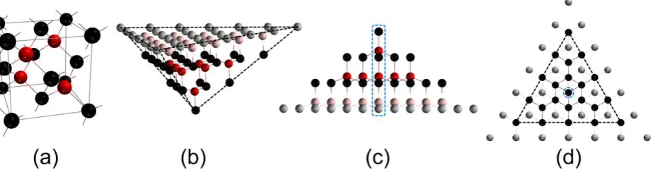
In order to calculate the tunneling current, the STM tip was modeled using the well-known diamond lattice structure (Fig. 6(a)) [30]. This crystal structure can be represented as a set of two interpenetrating face-centered cubic lattices shifted along the cube diagonal by 1/4 of the lattice parameter. The basis of the Bravais lattice of the diamond crystal structure consists of two atoms with coordinates 0,0,0 and 1/4, 1/4, 1/4. Fig. 6(b) shows a model of the pyramidal apex of the diamond tip, which can be described as a system of straight parallel atomic chains with equal interatomic distances, as Fig. 6(c) illustrates. Because of the high stability of the diamond atomic structure, the calculation of the tunneling current within this model can provide reliable information about the tunneling parameters necessary for stable imaging with atomic resolution using single crystal diamond probes.
Since the tunneling current depends strongly on the distance between the tip and sample atoms [3, 15, 31, 32], the main contribution comes from only those tip atoms closest to the surface. The diameter of the interacting area is limited to the diameter of the tunneling channel. For atomic resolution STM experiments, this cannot substantially exceed the interatomic distance in the probe’s crystal lattice. In our calculations, 29 atoms of the diamond tip’s apex are taken into consideration (Fig. 6(c) and 6(d)). The atomic structure shown in Fig. 6(c) allows us to model the crystallattice of the diamond tip as a set of non-interacting, semi-infinite chains of spherical potential wells, and calculate the tunneling current on the basis of the LS formalism [13, 26]. The
separation between the chains is equal to the diagonal of the diamond cubic cell (Fig. 6(a)). The surface is simulated by the Green's function, which is included in the LS-equation. The presence of boron atoms in the carbon diamond structure provides no tunneling conductance in the barrier between the electrodes, but it gives the diamond crystal the electrical conductivity necessary for use as an STM probe. When the boron concentration does not exceed 0.1%, the probability of its appearance within the interacting area of the tip does not exceed 0.01. Therefore, the presence of boron atoms at the apex is not considered in our calculations.
The procedure for the calculation of the tunneling current reduces to the summation of the contributions from chains of spherical potential wells formed at the apex of a diamond tip (Fig. 6(c,d)). The calculation of the tunneling current in the system of "semi-infinite chain of spherical potential wells – sample surface," is performed by means of the non-perturbative approach that is described in detail in [26]. However, in contrast to the one-dimensional tip model used in Ref. [26], we analyze the three-dimensional structure of spherical potential wells forming the diamond lattice (Fig. 6(b)).
The equation for the tunneling current proposed on the basis of [26] has the form:
. ) , ( * ] [ 1 ) , ( ] [ Im 4 2 0 0 0 0 2
i i i L i i i L i t r r g D D r r D D V e I (1)
Here, the summation is applied to all chains of potential wells that make up the diamond tip.
i isproportional to the reflection coefficient of electron
waves from the i-th chain. The presence of
i in (1)implies that the electron waves reflected from the tip are taken into account. The electron wave function
inc
, which describes the tunneling electrons incident to the tip, can be expressed using spherical harmonics [26]: ) ( ) ( ) ( , , ,
r D j ikuYlm u
m l l m l inc , i
r
r
u
0
[image:5.595.79.541.62.184.2]inc
is represented as a superposition of the wave function of the surface
L and the function
,corresponding to the reflected electrons:
inc L . The summation in equation (2) iscarried out over the quantum numbers (l, m) of the
magnetic moments of the electrons. The vector
r
0i
in
(2) denotes the location of the nearest to the surface spherical potential well of the i-th chain, and k is a modulus of the wave vector of the tunneling electron.
The operator
D
, in (1) determines the expansion coefficients,D
l,m, in (2):)
(
0,m inc i
l
D
r
D
, (3)
l l m l lr
u
Y
d
ik
l
l
D
(
)
(
)
!
!
)!
1
2
(
* ,
(4)In the numerator of equation (1), this operator acts on the LDOS of the surface:
)
(
2
L
LE
E
(5)where E is the energy of tunneling electrons and the summation takes into account the contribution of all
electron states involved in tunneling.
L is associated with the surface Green’s function)
,
(
r
r
g
L
that is a part of the LS equation:
)
(
)
,
(
)
(
)
(
r
Lr
V
0d
3r
g
Lr
r
r
(6)
The function
(
r
)
in equation (6) is the total wave function of the tip-sample system.V
0 is thedepth of the potential wells, simulating the carbon atoms in the diamond tip, and τ is the volume of each of these wells.
The Green’s function
g
L(
r
,
r
)
is presented in
the form of two terms [26]
g
L
g
f
g
L, wherethe free-particle function
g
f describes free electronsand
g
L corresponds to the surface electrons. ForL
g
we used the Green’s function proposed in [33]:2 0 2 2 0 2 2 0 ) ( ) ) ( exp( ) 0 ( 2 ) , ( i i z z z z k r m r r gL
(7)
where
i
x
x
0
andz
are the polar and z-coordinates, respectively, of the radius vectorr
of the electrons.The surface was taken into account using the Green's function (7), and the Fermi level of graphite was used in order to directly compare the tunneling current calculations with the results of STM experiments (Figs. 2 and 3). Using equation (1) the current calculations were performed for different bias voltages and tip-sample distannces. The tip-surface distance dependence of the tunneling current obtained using the presented model is shown in Fig. 7. It reaches a maximum at a distance ~1.5 Å from the surface, due to the factors in the denominator of equation (1), which are related to the reflection of electron waves from the tip and the sample during the tunneling process.
The extreme behavior of the tunneling current at small distances contradicts the exponential function given by perturbation theory. The non-exponential behavior of the tunneling current was experimentally observed by Gimzevski and Möller [34] and explained by the probe "jumping" to the surface under the action of adhesive forces. However, as follows from the present work, the presence of the maximum in the current-distance dependence can be explained by the reflection of electron waves between the probe and the sample, without needing to include additional forces. The resonance behavior of the tunneling current at small distances is important for the explanation of STM images recorded in the near contact regime.
The results of It(Zt) calculations can be used to estimate the maximum noise in the tunneling current channel which will still allow atomically resolved STM experiments. Evidently, higher errors in the Figure7. The dependence of the tunneling current Iton the distance Ztbetween the diamond probe and the graphite surface at a
sample bias voltage of 0.1 V. Is+p– total tunneling current It taking into account both s and p electrons. Ipand Ipz are partial
currents due to only the p and pz electrons, respectively. At small distances (a) the tunneling current reaches a maximum, due
tunneling current registration are still allowable for reaching atomic resolution at stronger current-distance dependence. The errors in the measurement and control of the tunneling current can be estimated using the formula:
dZ
Z
I
Z
I
Z ZZ
Z t
t t
t t
(
)
(
)
, (8)where Zt is the tunneling gap spacing and ΔZ is the maximal allowable error in the measurement of the Z -position of the tip scanning across the surface (note that ΔZ is typically below 0.1 Å for atomically resolved imaging on metals and on the order of 0.1 Å for semiconducting atomic structures).
It can be suggested from formula (8) and Fig. 7 that reliable STM images with the highest spatial resolution can be measured with a diamond probe at small tip-sample distances exceeding the distance where the maximum in the current-distance dependence is observed. This corresponds to a tunneling gap in the range of 2.5–5 Å. At smaller distances the deviation from the exponential law suggests the presence of possible artifacts due to the decreasing tunneling current with decreasing distance. At distances above 5 Å, the noise in the It and Zt channels can be comparable to the atomic corrugation. As a result, lower contrast in STM images can be expected at large tunneling gaps. Using equations (1) and (8) and the method of evaluating the reliability of STM topograms [35], it can be concluded that stable, atomically resolved imaging with single crystal diamond probes can be achieved if the instrumental errors in maintaining a constant tunneling current do not exceed 3%, and the tunneling gap is in the range of 2.5–5 Å.
IV. Discussion
The gap resistance dependence of STM images measured with a diamond tip on a graphite (0001) surface (Fig. 3) qualitatively agrees with the estimations based on equation (8) and the current-distance dependence shown in Fig. 7. STM images with a lower signal-to-noise ratio were measured at larger gap resistances (Figs. 3(a) and 3(f)), while high contrast, atomically resolved images were recorded at tunneling currents in the range of 0.1–1.0 nA (e.g., Fig. 3(c) and 3(d) show images measured at U = -0.1 V, It = 0.3 nA and U = -0.1 V, It = 0.5 nA, respectively). According to the theoretical calculations (Fig. 7), these tunneling parameters correspond to tip-sample distances of 3.0–3.5 Å. With a further increase of the tunneling current, the noise level is substantially increased because of strong tip-sample interactions and graphite surface layer oscillations [36]. Despite the high noise level, atomically resolved STM images still could be measured at currents up to 3.0 nA (not shown in Fig. 3), which correspond to tunneling gaps of about 2.5 Å. At higher currents (smaller distances), regular atomically resolved patterns were not discernible because of possible artifacts related to the
non-exponential current-distance dependence predicted for tunneling gaps below 2.0 Å (Fig. 7(a)).
Another source of this unstable atomic contrast at very small tip-sample distances is related to the substantial modification of the surface and tip atoms’ PDOS because of the overlapping of the tip and surface atomic orbitals. This is illustrated by the distance dependences of the surface atoms’ PDOS calculated for three different lateral positions of the diamond tip (Fig. 5). The surface electronic structure is not significantly disturbed at tip-sample distances above 3.5 Å for all lateral positions of the tip. The situation is changed at tip-sample separations below 3.0 Å. It is clear from Fig. 5 that at these distances, the PDOS both the α and β atoms is substantially modified when the tip is placed above the corresponding surface atoms. The surface pz electron states at the Fermi level are essentially suppressed because of the overlap of the pz-orbitals of the tip and surface atoms. At the same time, the electronic structure of the α and β atoms is practically unchanged when the tip positioned above the hollow site at distances exceeding 2.0 Å (e.g. the PDOS of the β atom closest to the apex atom at a 2.5 Å tip-surface separation in Fig. 5). Because of the spatial distribution of the carbon pz-orbital, the overlap of the atomic orbitals of the foremost tip atom and the surface atoms does not take place for the tip position above the center of the hollow site.
As can also be suggested from the distance dependence of the tip and surface PDOS for the three lateral tip positions, the relative contributions of the
pz and pxy orbitals of the tip and surface atoms involved in tunneling can change while scanning the tip in the x-y plane at tip-sample distances below 2.5 Å. At larger distances, stable imaging of the graphite surface’s pz-orbitals by the diamond tip’s pz-orbital can be suggested.
Another effect observed in Fig. 3 is a reversible change of contrast from the honeycomb to the hexagonal pattern with increasing gap resistance (increasing tip-surface distance). Comparing the values of tunneling currents in Fig. 3 with the theoretical current-distance dependence in Fig. 7(b), one can conclude that this contrast reversal may take place at tip-sample distances in the range of 4.0–4.5 Å. This is in qualitative agreement with the results of earlier theoretical calculations performed for the graphite (0001) surface and a tungsten tip [27], suggesting the transition from imaging the surface carbon atoms to imaging the hollow sites due to multiple scattering effects in the tunneling gap. The gap resistance dependence of the graphite STM images measured with the diamond tip (Fig. 3), the PDOS of the tip and surface atoms as a function of the tunneling gap and lateral tip position (Figs. 4 and 5), and the distance dependence of the tunneling current (Fig. 7) suggest that the highest resolution STM images with honeycomb patterns (Fig. 2(b)) could be resolved with diamond probes in a distance range of 4.0–5.0 Å. According to Figs. 4, 5 and 7, this distance range corresponds to imaging the surface pz-orbitals with the diamond tip atom pz -orbital.
Fig. 5 reveals a minor difference in the DOS corresponding to the α and β-atoms of the graphite surface. The DOS at the Fermi level is larger for β atoms by ~25%, and the difference slightly decreases for the DOS integrated over a wider range of electron energies. This difference is responsible for the two non-equivalent sublattices of carbon atoms observed in STM images shown in Figs. 2(b) and 2(c).
As can be assumed from the DFT calculations (Fig. 4), at tip-surface separations above 4 Å the interaction between the tip and sample is small. In this case equation (1) resembles the Tersoff and Hamann approximation [1]:
) ( ~ )
( t L t
t Z Z
I
(9) Using (9) and the difference in the density of states of the α and β-atoms at the Fermi level (Fig. 5), we can estimate the height difference between the α and β-sublattices of the atomic structure observed in Fig. 2(b). At a tunneling current value of 0.1 nA and a bias voltage of -50 mV, the calculated difference is 0.15 Å, in very good agreement with the experimental data (see the cross-section in Fig. 2(d)). The smaller height difference observed in the STM image measured at U = -0.4 V with the W[001] tip (Fig. 2(e)) is also in agreement with the decreasing difference in the density of electron states of the α and β atoms integrated over the corresponding energy range.V. Conclusions
We have presented the results of STM experiments performed with boron-doped, single crystal diamond probes on a graphite (0001) surface and the theoretical calculations of the tip and surface
electronic structure and the tunneling current in the tip-surface system. The current has been calculated on the basis of the non-perturbative approach, which can be applied at any tunneling gap, including extremely small gaps (1.5–2.5 Å). The tunneling current exhibits a maximum at tunneling gaps below 2 Å. This deviation from the exponential law is related to the reflection of electron waves in the tunneling gap rather than a jump-to-contact with decreasing distance. This non-exponential dependence can lead to artifacts and the loss of atomic resolution in STM images measured at extremely small tip-sample distances (2.0 Å and below). The tunneling current calculations show that if the instrumental errors in maintaining a constant tunneling current do not exceed 3%, and the gap width is in the range of 2.5–5.0 Å, atomically resolved imaging with a diamond probe is feasible. The distance dependences of the tunneling currents corresponding to different tip atomic orbitals show that the pz-orbital of the tip provides a major contribution at separations exceeding 3.0 Å and, therefore, can define the spatial resolution in experiments at these tip-surface distances. STM experiments and theoretical calculations show that the best atomically resolved images that reproduce the honeycomb lattice of the graphite surface can be measured at distances in the range of 4.0–5.0 Å, corresponding to imaging of the surface pz-orbitals by the tip atom pz-orbital. The experimental images obtained with conductive single crystal diamond probes demonstrate the advantages of the tips with a
pz orbital at the apex. Although picometer lateral resolution has recently been demonstrated in STM experiments with single crystalline tungsten probes [37], the further z-extension of the carbon pz-orbital allows for higher vertical resolution and sub-Ångström lateral resolution at larger distances than applied in high resolution experiments with transition metal probes. Because of the reduced tip-sample interaction at these distances, the tip state and pz -orbital contribution can be controlled using oriented single crystal diamond probes.
Acknowledgments
This work was supported by the State Target Scientific and Technical Program "Nanotechnology and nanomaterials" project №2.2.11.31, by the Russian Academy of Sciences, RFBR grant №11-02-01256 and Marie Curie IIF grant within the 7th European Community Framework Programme. STM images were processed using WSxM software [38].
References
[1] Tersoff J and Hamann D R 1985 Phys. Rev. B 31
805-813
[2] Chen C J 1990 Phys. Rev. Lett.65 448-451 [3] Hofer W A, Redinger J and Varga P 2000 Solid State Communications113 245-250
[4] Tersoff J and Lang N D 1990 Phys. Rev. Lett.65
[5] Vazquez de Parga A L, Hernan O S, Miranda R, Levy Yeyati A, Mingo N, Martin-Rodero A and Flores F 1998 Phys. Rev. Lett.80 357-360
[6] Cerda J, Yoon A, van Hove M A, Sautet P, Salmeron M and Somorjai G A 1997 Phys. Rev. B 56
15900-15918
[7] Hofer W A and Redinger J 2000 Surf. Sci. 447
51-61
[8] Chaika A N, Semenov V N, Nazin S S, Bozhko S I, Murphy S, Radican K and Shvets I V 2007 Phys. Rev. Lett.98 206101
[9] Murphy S, Radican K, Shvets I V, Chaika A N, Semenov V N, Nazin S S and Bozhko S I 2007 Phys. Rev. B 76 245423
[10] Chen C J 1990 Phys. Rev. B 42 8841-8857 [11] Sacks W 2000 Phys. Rev. B 61 7656-7668 [12] Sacks W and Noguera C 1991 J. Vac. Sci. Technol. B 9 488-491
[13] Lippmann B A and Schwinger J 1950 Phys. Rev.
79 469-480
[14] Bardeen J 1961 Phys. Rev. Lett.6 57-59
[15] Hofer W A, Foster A S and Shluger A L 2003 Rev. Mod. Phys. 75 1287-1331
[16] Doyen G, Drakova D and Scheffler M 1993
Phys. Rev. B 47 9778-9790
[17] Ness H and Fisher A J 1997 Phys. Rev. B 56
12469-12481
[18] Herz M, Giessibl F J and Mannhart J 2003 Phys. Rev. B 68 045301
[19] Chaika A N, Nazin S S, Semenov V N, Bozhko S I, Lübben O, Krasnikov S A, Radican K and Shvets I V 2010 EPL92 46003
[20] Chaika A N, Nazin S S, Semenov V N, Orlova N N, Bozhko S I, Lübben O, Krasnikov S A, Radican K and Shvets I V 2013 Appl. Surf. Sci.267 219-223 [21] Gross L, Moll N, Mohn F, Curioni A, Meyer G, Hanke F and Persson M 2011 Phys. Rev. Lett. 107
086101
[22] Weiss C, Wagner C, Kleimann C, Rohlfing M, Tautz F S and Temirov R 2010 Phys. Rev. Lett.105
86103
[23] Hofmann T, Welker J, Giessibl F J 2010 J. Vac. Sci. Technol. B 28 C4E28
[24] Lysenko O, Novikov N, Grushko V, Shcherbakov A, Katrusha A and Ivakhnenko S 2008
Diamond Rel. Mat.17 1316-1319
[25] Lysenko O, Novikov N, Gontar A, Grushko V and Shcherbakov A 2007 J. Phys.: Conf. Ser. 61 740-744
[26] Sacks W and Noguera C 1991 Phys. Rev. B 43
11612-1622
[27] Ondracek M, Pou P, Rozsival V, Gonzalez C, Jelinek P and Perez R 2011 Phys. Rev. Lett. 106
176101
[28] Kresse G and Furthmüller J 1996 Phys. Rev. B
54 11169–11186
[29] Ceperley D M and Alder B J 1980 Phys. Rev.
Lett.45 566–569
[30] Egon W, Nils W and Frederick H A 2001
Inorganic chemistry. Academic Press, ISBN 9780123526519
[31] Simmons J G 1963 J. Appl. Phys.34 1793-1803
[32] Richter A and Smith R S A 2003 Cryst. Res. Technol.38 250-266
[33] Hurault J P 1971 J. Phys. (Paris)32 421
[34] Gimzewski J K and Möller R 1987 Phys. Rev. B
36 1284-1287
[35] Grushko V 1996 Technical diagnostics and non-destructive testing2 17
[36] Binnig G K 1987 Physica Scripta T 19A 53-54 [37] Chaika A N, Molodtsova O V, Zakharov A A, Marchenko D, Sánchez-Barriga J, Varykhalov A, Shvets I V and Aristov V Yu 2013 Nano Research
DOI – 10.1007/s12274-013-0331-9
[38] Horcas I, Fernandez R, Gomez-Rodriguez J M, Colchero J, Gomez-Herrero J and Baro A M 2007