OPERATING MANUAL
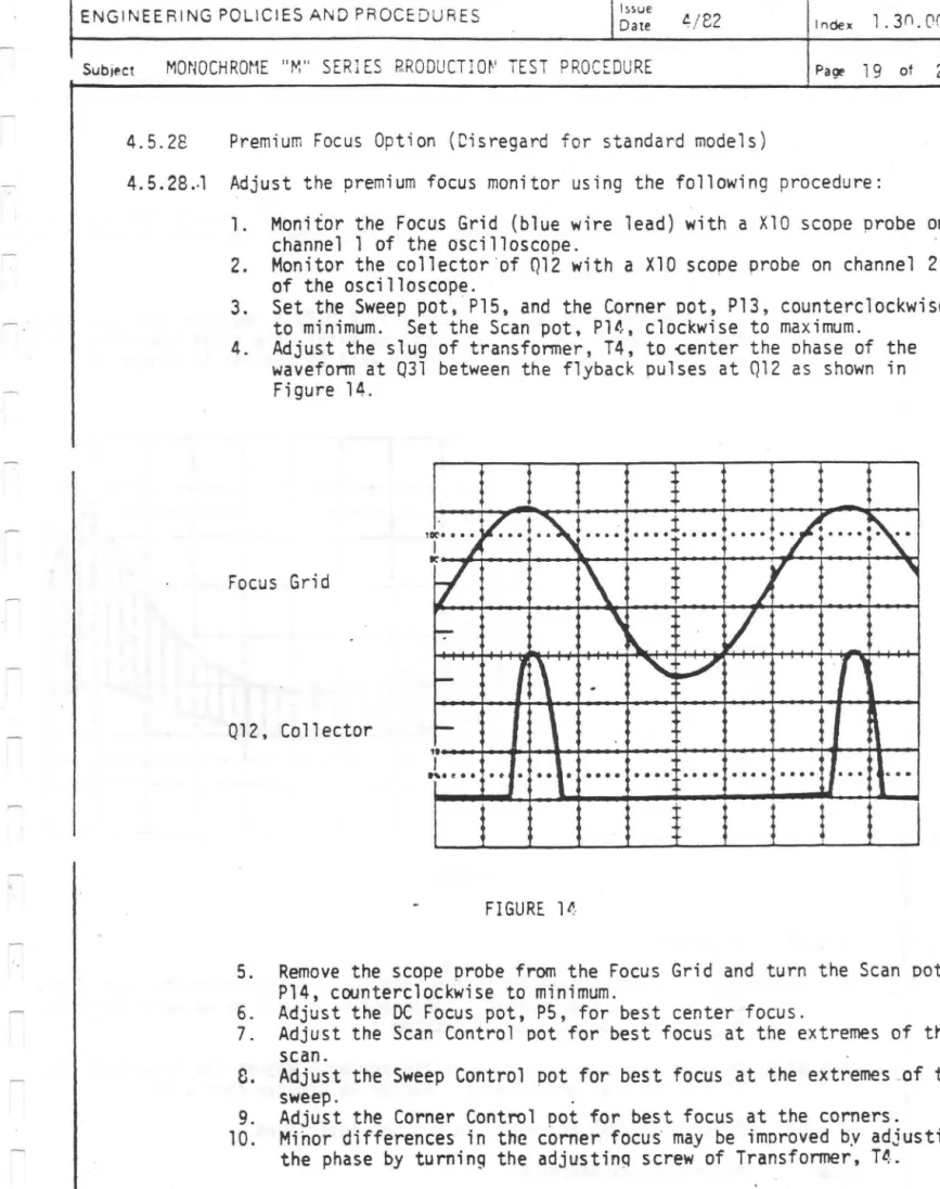
l
SERVICING AND OPERATING SAFETY
GROUND THE PRODUCT SECURELY
This product is designed to be grounded through the chassis. To avoid electrical shock, extreme care should ~ be used to ensure that the chassis is solidly grounded. Units with the AC power supply option may be grounded through the grounding connector of the power cord.
CAUTION: upon loss of the protective ground connection, all accessible conductive parts can
render an electric shock.
USE THE PROPER FUSE.
To avoid fire hazard, use only those fuses of the correct type, voltage rating, and current rating as specified
in the parts list for your product.
l
00 NOT OPERATE IN AN EXPLOSIVE ATMOSPHERE
To avoid explosion, do not operate this product in an explosive atmosphere.
DO NOT SERVICE THIS PRODUCT ALONE
00 not perform internal adjustment or service of this product unless another person capable of rendering first aid is present.
USE CAUTION WHEN SERVICING WITH THE POWER ON
Dangerous voltages are present at several points in this product. To avoid injury, do not touch expose< connections and components while the power is on.
Disconnect power before soldering or replacing components,
USE THE PROPER POWER SUPPLY
'This product is designed to operate with a power supply that will supply no more than 250 volts rm~ between the supply conductors or between either supply conductor and ground.
SECTION I . GENERAL INFORMATION
. 1 MONITOR DESCRIPTION
-The M series monitor is a solid-state display for use in systems requiring exceptionally high quality video.
)rinted circuit board construction coupled with the all solid-state circuitry provides high reliability and uniforrflity Synchronization circuitry has been designed to simplify the interfacing of this monitor with users systems_ Separatl'
- ,ertical and horizontal sync signals are used to eliminate the need for composite sync generation in the stafldarc mit.
Composite sync is available as an option.
1.2 ELECTRICAL SPECIFICATIONS
j SPECIFICATIONS INPUT DATA VIDEO
,PULSE RATE OR WIDTH 11 nsec.
I
AMPLITUDE Black • OV_ ~INGlE ENDED White - .7V
eCL DIFFERENTIAL Low - - .9V
OPTIONAL High ,. - 1.35V
- RISE AND FALL 5 nsec. max. (10% - 90%)
INPUT SIGNAL
- COMPOSITE 0.7V min. 2.0V max.
J
CONNECTOR Edge 10 PIN Card Ribbon (ECU 10 PIN SPECIFICATIONS tonch~"'" I3oC7':J.3DDO
Of EQ.) arEQ)
I
HORIZONTAL SYNC 9,
VERTICAL SYNC 10 3
VIDEO POSITIVE 1 5
'IDEO NEGATIVE N/C 6
- GROUND AF 2.4.7,10
~ BRIGHTNESS POSITIVE 7 ,
BRIGHTNESS NEGATIVE 8
,...J BRIGHTNESS WIPER 6
KEYWAY 3
CONTRAST 2
INPUT IMPEDANCE MINIMUM
t RESISTANCE
Single 75 Ohm or
I VIDEO INPUT Ended 20 K Min.
Switch .Iecubl.
Eel Input 112 Ohm
,...Ji- · Balanced
One LS-TTl
'ORIZONTAL SYNC load
-
~
VERTICAL SYNC One LS-TTLj. load
VERTICAL SYNC HORIZONTAL SYNC
49-61/sec. See specific model detail~
- ~
low - 0 + 0.4 -0.0 Volts Hig, - 4 ±. 1.5 Volts
100 nsec. max. 100 nsec. max.
See Figure No. ,
35-45% of video amplitude
.~
POWER REQUIREMENTS
MONITORS USING AN EXTERNAL DC POWER SU:;PlY
.
_
-INPUT CONNECTOR Molex: ReceptaCle «l:h'19-1022(Pin tr2 is positive " god) 0209'103 -1 ea. 02042102 . , ea.
INPUT VOLTAGE" 55V to 70VDC INPUT CURRENT See specific model >#-• Internal regulation IS provided
MONITORS WITH INTEGRAL POWER SUPPLY INPUT VOLTAGE 100.120,220, 2fJJV RMS
5QI6O Hz switch selectable
INPUT POWER 125W (NominaO See specific
~!...-NOTE: Power transformers must be of low 0 -ternal flux design or well removed from CRT.
~I.I ':' f '.' ""
VIDEO AMPLIFIER
Rise and fall time
(10-/0 to 90% amplitude)
LINEARITY
Vertical and horizontal linearity will be
within ~ 1 % of the major axis.
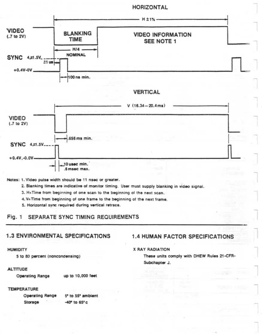
HORIZONTAL
~I.~--- H±1%~---~·1
VIDEO
(.7 to 2V)
----,
BLANKING
TIME VIDEO INFORMA nON SEE NOTE 1
SYNC ',o1.SV_ !-,_ .""OMINAL
tn
H/4 -,+O.4V~V
___________~
L. ____________________________________________________~~
VIDEO
(.7 to 2V)
Hoonamino
u
VERTICAL
V (18.34-2004ma)
L
1----1
.
656
ms min.I
SYNC ... SV ___
-n
L
+O.4V,-a.OV '
-_I
L10 UMC min.-I
,-.8
msec max.Notes: 1. Video pulse width should be 11 nsec: or greater.
2. Blanking times are indicative of monitor timing, User must supply blanking in videa signal.
3. H:;nme from b89inninq of one scan to tha beginning 01 the next scan.
4. V .. TIme from beginning of on6 frame to the beginning of the next fram •.
5. Horizontal sync required during vertical retrace,
Fig. 1 SEPARATE SYNC TIMING REQUIREMENTS
1.3 ENVIRONMENTAL SPECIFICATIONS
HUMIDITY
5 to 80 perc;ent (noncondensing)
.ALTITUDE
Operating Range up to 10,000 feet
TeMPERATURE
Operating Range 5° to 5S' ambient
Storag. -.we to 65' c
1.4 HUMAN FACTOR SPECIFICATIONS
X RAY RADIA nON
These units comply with CHEW Rule.
21-CFR-Subchapter J .
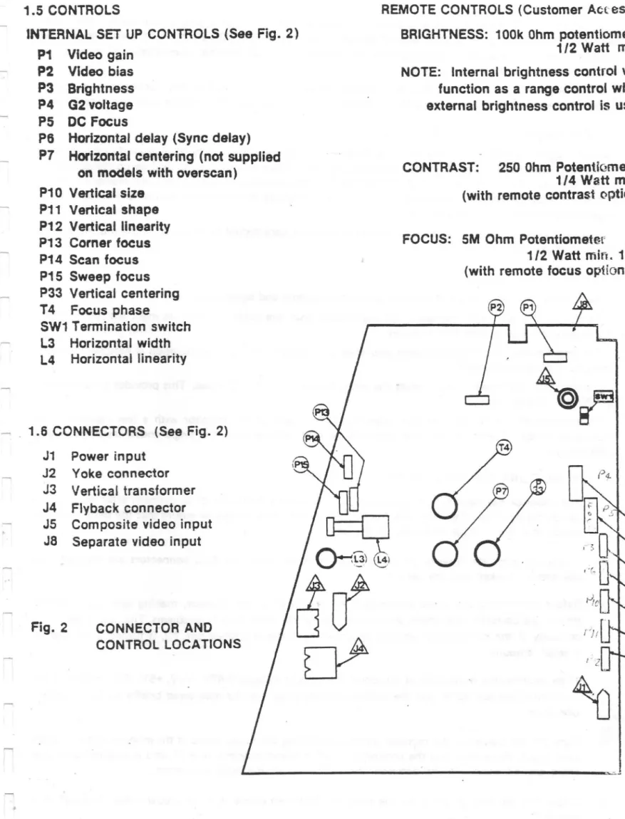
1.5 CONTROLS
1NTERNAL SET UP CONTROLS (See Fig. 2)
P1 Video gain P2 Video bias
P3 Brightness P4 G2 voltage
P5 DC Focus
P6 Horizontal delay (Sync delay) P7 Horizontal centering (not supplied
on models with overscan) P10 Vertical size
P11 Vertical shape P12 Vertical linearity P13 Corner focus
P14 Scan focus
P15 Sweep focus P33 Vertical centering
T 4 Focus phase
SW1 Termination switch L3 Horizontal width L4 Horizontal linearity
1.6 CONNECTORS (See Fig. 2) J1 Power input
J2 Yoke connector J3 Vertical transformer J4 Flyback connector
J5 Composite video input
J8 Separate video input
Fig. 2 CONNECTOR AND
CONTROL LOCATIONS
REMOTE CONTROLS (Customer Ac(:es~
BRIGHTNESS: 100k Ohm potentiome
112 Watt m NOTE: Internal brightness control V\
function as a range control wh external brightness control is us
CONTRAST: 250 Ohm Potentiomet
1/4 Watt mi
(with remote contrast optic
FOCUS: 5M Ohm Potentiomeh~l'
1/2 Watt min. 1~
INSTALLATION
SECTION 2
OPERATING PROCEDURES
Power for the M series monitors is supplied in one of two ways, depending on the model. The model with bu ilt-in low voltage supply is powered directly from 120 V AC (100/2201240 V AC switch selectable). Units without a built-in low voltage supply are supplied from an external unregulated DC supply. See
. section one for connector assignments.
Video and sync signals are fed to the appropriate pin as in section one connector descrjption. Mount the monitor so that the ambient temperature surrounding the monitor does not exceed 55°c.
2.2 GROUNDING TECHNIQUES
Arc bypasses are returned to ground at the origin of the driving signals. In tum, all grounds are connected
to the monitor chassis. Normally, it is assumed that the chassis of the monitor will be connected to the system ground via the mounting. If this is true, no further grounding should be required. However, ground pins are provided in the lID connector and should be connected to the driving source to maintain proper
impedances and minimize cross talk in the cable. -,
,
"'
Due to the high frequency video supplied to the monitor, care should be exercised in the routing and the shielding of the I/O cable.
2.3 VIDEO LEAD
Make the video lead as short as possible to minimize pickup and signal distortion.
As the video lead length increases, the importance that the cable be made to meet the requirements of a terminated transmission line increases.
For single ended input units utilizing gray scale capabilities, the input termination is switched between 75 ohms and high impedance.
For the Etl differential input units the input termination is 112 ohms. This provides a close match to 120 ohm ribbon cable.
Observation of the response of the video should be made at the monitor with a low capacity, high impedance probe. Overshoot and rise time will be most critical with the single ended input with gray scale displays.
2.4 INITIAL TURN ON PROCEDURES
1. The monitor has been factory calibrated, and requires a minimum of adiustment aher installation. Ch~k the position of switches SW·' and SW-2 on the power supply to ensure that the switch settings match the line voltage available to the unit.
2. Visually inspect the interior of the monitor to make sure that ALL connectors are plugged into the proper socket and are secure.
3. Before connecting any video connecto~, apply power to the monitor, making sure that monitor powers up correctly and enters the free-run operating mode with no problems. The unit is operating correctly if the background raster is apparant when the brightness pot, P3, is turned clockwise by a small amount.
If an oscilloscope is av~ilable at this point, the supply voltages (+48V, +HV, +5V, -5V, and +6V), the horizontal fly back pulse, and the vertical flyback pulse may be monitored briefly to verify correct operation.
4. Tum off the po~er to the monitor before connecting the video input. If the monitor has a separate
l
l
sync input, make sure that the connector to J8 is keyed properly (pin 3), and is inserted such that
l
there are no short circuits between adjacent pins on the edge connector.Apply the video signal to the unit, and then apply power to the unit.
Allow approximately 15 minutes to warm-up.
Adjust the video bias to the DC level specified by the unit specification using the bias pot, P2.
Adjust the video gain to the range specified by the unit specifications using the gain pot, P1.
Center the picture within the screen by adjusting the horizontal delay pot, P6.
Adjust the brightness of the image to the desired level by adjusting the brighmess pot, P3. (If an external brightness control is being used, adjust the internal control to provide the desired range on the external control).
< VIDEO AMPLIFIER
SECTION 3
THEORY OF OPERATION
fhe video amplifier consists of an input buffer, a differential input transistor pre-amplifier, and ft high
::===='ilI7lSl:iltage cascade output stage.
-th
e
input buffer consists of transistors 04 and 015 acting as emitter followers to providea
high input----t-i.ftrr'iledance to give isolation and minimize loading of the drive signal. The output from the emitter of
Q; 5 is AC coupled to the pre·amplifier through capacitors C1 and C2. Gain control is provided by P1
----1tr."lich can be adjusted to give a 5 to 1 attenuation. The diode CR5 acts as a clamp to provide DC
. __ h_Jettoration to maintain the black level.
i!te pre·amplifier is a differential ampl ifier comprised of 01 and 03. The base of Q3 is connected to a
-:: f'f?ierence voltage which is set by P2. Transistor 01 drives the base of 02, and the collector of Q2 provides
=--:-:~ output of the pre-amplifier. The peramp has a nominal gain of 3, which is controlled by R5 and R6.
" t4~sistor R6 sets the basic gain of the preamp. Resistor R5 provides feedback to the emitter of the output
=-=:~~it$lta .. ge for stability and gain control. R 12 and C3 provide high frequency compensation for the preamp.
}f
any additional compensation is needed, C26 is added. Diode CR1 gives base protection to 01. ResistorK
I
'
acts as the load resistance to the circuit.-,r-::-ansistors 07 and 08 form the differential amplifier which is the driver for the output stage. In the output
- =====--3ge, the output signal from the preamp is applied to the base of 07. Transistor Q8 provides bias reference
---- --.=-;0 temperature compensation. The gain is set by R22 and R23. Capacitor C10 couples resistor R21 with
--:--::-~~ and R23, to provide high frequency boost gain. Transistor 07 operate~ in the linear mode with a
-;--- -:nimum quiescent current of approximately 30 rna. The collector of 07 drives the emitter of 06 which
.- ~: connected as a grounded base with its base biased at +5 volts. The 30 rna. quiescent current of 07 keeps
&-6
from being completely turned off, thus holding its collector voltage at approximately 40 volts.-rite bias control, P2 is used to adjust the quiescent operating point of the Q6 collector. With the input
-- a positive video signal, the 07 collector current will rise, thus lowe~ing the video output voltage. This-.. ill cause the screen to display a white signal. Note that too high a video signal will cause Q6 to ~i.llrate . ·--==:=:1d the resulting excessive turn-off times will result in smearing of the white to black transitions;
---__ ~urrent through inductor L5 provides boost or peaking voltage. The diode CR4 clamps to 48 V(Jlts to
.- _===:l. otect Q6 from arcs. Resistor R 17 and the 48 ohm resistor provide current limiting against arc tran~it;nts..
::===::;; ;~omponent AG 1 is a neon arc gap, which fires at 70 to 75 volts, providing voltage protection agairlst arc ===4trr:aansients .
. __ --=2 HORIZONTAL DEFLECTION
.
~tn 12 of one shot Z 1, and Pin. 13 of one shot Z2 are outputs of the two sections of the hori2lmtal -===::::I!'SliC:illator. In the absence of the horizontal sync input, this oscillator will free-run at a nominal frequency
.... ::wtiG1i ...
::wvn
ich is approximately 10 percent faster than the locked-in frequency. When horizontal sync signal is- • l:sented to pin 2 of Z 1, the oscillator locks into synchronization with the input signal with a phase
Pin 5 of Z2 is the output pin of the drive section of the osciilator The pulse width of this se:::tion is se1 ll'
provide a duty cycle of approximately 40 percent at the locked-in frequency.
Transistor 010 is an emitter follower buffer which supplies sufficient current gain to drive 011. Transistor Ql1 is an inverter. When the voltage from pin 5 of Z2 rises, 010 turns on, supplying current to 011 whict also turns on, pulling current through the primary of transformer T3. Since the primary of T3 acts as an inductor, no current flows initially, and thus the voltage at the collector of 011 is pulled down. This accomplished four objectives:
1.) Energy is stored in 13
(This energy will be used to turn 0'12 on during the second half of the cycle.) 2') The base of Q12 is driven negati~ning 012 off quickly.
3,) A positive pulse is driven through diode CR23 charging capacitor C53 giving raw 10 volts. 4.) Current flows through CR24 which charges C51 to produce minus 5 voltage supply.
(CR24 is also used to protect the base against overshoot.)
Diode CR25 is present to provide a low impedance path during turn-off to drive the base of Q12 harder. Inductor LI is a high frequency filter for the minus 5 volt supply.
When the voltage from pin 5 of Z2 drops, 010 turns off, which causes 011 to tum off. The inductiVE: energy present in T3 swings the collector of 011 positive to approximately 90 volts. Diodes CR21, and CR22 provide over-voltage protection to 011 by clamping at 100 volts, via a zener drop through CR21 to 48 volts. In normal operation, the collector of 011 will never reach 100 volts.
Th is voltage rise causes the base of 012 to be driven positive at a 1:8 voltage ratio. The amount of base current is determined by R61. (Base current is approximately 0.4 amps when 012 is an MJ10009, and is approximately 0.2 amps when 012 is an SVT6253.)
Capacitors C46, 47, and 48 provide AC decoupling. RS9 and C49 form an AC snubber, which prevents voltage at the collector of 011 from rising instantaneously. This provides noise reduction and reduces -.,
dissipation in 011. Resistor R61 provides current limitation during start up. 3.3 HORIZONTAL OUTPUT
Shortly before the end of the sweep, while the beam is at the right hand side of the screen, 012 is still turned on, effectively shorting C64 and C6S. At this time the currents from the fly back transformer T2, the yoke L2, the width coil, L3, and the linearity coil L4, are flowing into the collector of 012. When horizontal sync arrives and 012 turns off, current continues to flow through T2, L2, L3, and L4 due to tht energy stored by the inductance of these components. This current charges up capacitors C64 and C6S, which are no longer shorted out by 012. Thus the voltage across capacitors C64 and C65, rises until the energy in T2, L2, L3, and L4 is depleted. At this point, the current through the inductors is zero and the voltage across C64 and C65 is at a maximum (approximately 450 volts), the middle of the flyback has beer
reached and the beam is in the center of the screen.
Once the energy in the coils has been discharged into the capacitors, the current reverses, and begins
flowing from the capacitors back into the coils. This process constitutes the second half of the flyback operation. Current continues to flow back into T2, L2, L3, and L4 from the capacitor until the voltag£~ across the capacitor reaches zero. At this point, current flow into the windings is at a maximum. and the beam is at the left of the screen.
The current continues to flow in the reverse direction, through the yoke and the transformer and would tend to charge C64 and C6S in the reverse direction. This is prevented by the damping diode which is
internal to Q 12. These voltage and current waveforms are exhibited in figure 3.
The desired waveform for the current through the yoke is an "s" shaped curve as shown in figure 3. This is primarily because the beam must travel slower at the edges of the screen than it does in the center. This· waveform is approximated by the natural resonance of the tuned circuit that is formed by the yoke, L2, and the capacit~r, C62. Due to the resistances inherant in these devices, these oscillations decay at an exponential rate. Because .of this, the beginning of the sweep has more amplitude than the end of the sweep causing the left side of the sCreen to be too wide. This effect is compensated by the linearity coil.
The width coil, L3, is a variable inductor which varies the amount of current through the yoke, thus adjusting width. The RC network composed of R63 and C61, provides damping to eliminate osciliatiClf)s at the end of the flyback pulse.
Capacitor C62 is present for two reasons. First, it adds to the "s" shaped component of the current wave. form of the yoke. Second, its voltage waveform is the integral of the current waveform, thus giving the parabolic waveform used for dynamic horizontal focus.
3.4 F L YBACK OUTPUTS
Pin 1
=
G2 voltage=
1 kv during flybackCR 11 and C34 rectifies and filters the raw G2 voltage.
Pin 4
=
-150 V pulse during flybackThis is rectified and filtered by CR12 and C35. Resistor R43 provides current limitation to protect C R 12.
The second anode provides 17 kv to the CRT.
The raw G2 voltage is fed to P4, which adjusts the G2 voltage to approximately 750 volts.
P3 sets the brightness operating point of the external brightness pot on J8. Resistors R40 and R41 control the net range of the external brightness control. Capacitors C30, C32, and C33 are arc capacitors to control transients.
3.5 VERTICAL DEFLECTION
Vertical sweep is generated by a free running oscillator consisting of a programmable unijunction transistor and its associated circuitry. The three resistors, R79, R82, and R83, determine the switching threshold of the unijunction transistor, 021. Transistor Q20 operates as a switch which adds R79 to the circuit when the vertical sync pulse arrives to change the switching threshold of the unij~nction.
This oscillator free runs at a slightly lower frequency than the lock-in frequency. This free run frEiquency
is primarily determined by the RC network formed by R84 and C72 and C74 in combination with the switching threshold of the unijunction Q21.
Vertical size is adjusted by P10 which adjusts the supply voltage to the unijuntion. Transistor 022 acts as a buffer to drive Q23 without loading 021.
Feedback networks, R87, P12, and R86, Pl', C73 modify the ramp waveform which is the normal output
of the oscillator into an "s" shaped curve for vertical linearity.
Transformer T' provides DC isolation, impedance matching and curve shaping to drive the vertitCiI de. flection yoke.
R93 and P33 provide DC bias current through the yoke for vertical centering. Resistor R90 prvvides damping on the yoke at the end of retrace. The capacitor C76 integrates the current to give the vultage parabolla waveform needed for dynamic vertical focusing.
During retrace, current continues to flow through T1 causing the voltage to rise. C42 and C43 clam~s this voltage at 150 volts above the horizontal clamp of 100V (i.e. Vertical is clamped at 25V). This large positive voltage pulse reverses the current in the yoke and moves the beam from the bottom to the ibP of . the screen.
3.6 CRT PROTECTION CIRCUIT
In the event of a failure in the horizontal or vertical deflection electonics, the brightness voltage to the CRT is switched to -150 volts (black level) to prevent phospher bums on the CRT, face plate. This protE'ction .
Transistor Q25 supplies +48 volts to the top end of the brightness potentiometer. When Q25 is turned off the brightness voltage drops to ·150 volts, and the CRT screen becomes black .
. , normal operation both the horizontal parabolic waveform and the vertical parabolic waveform are present. The vertical parabolic waveform is presented to the base of transistor 026, causing this transistor to shut off once each vertical cvcle. This allows the horizontal parabola from C62 to activate transistor
024. Capacitor C68 is thus discharged each cycle, and transistor 025 remains turned on.
1n lhe event of a failure in the horizontal drive circuitry, the horizontal parabola will not be present at
the base of 024 to tum it on. This allows capacitor C68 to charge up, shutting off transistor 025, and
preventing damage to the CRT.
If the failure is in the vertical drive circuit, the vertical parabola will not be generated. In the situation,
capacitor CS1 will charge up, causing transistor 026 to saturate, which shorts out the base of 024. Thus 024 remains off, capacitor C68 charges up, transistor 025 shuts off, and the +48 volt supply to the CRT
is shut off.
3.7 STANDARD DYNAMIC FOCUS
The vertical focus parabola from C76 is supplied to the emitter of 032 through P15 which acts as an attenuator. CS8, and R 122 provide DC biasing.
The horizontal parabola from C62 is supplied to the base of 032 through P14 which acts as an attenuator.
RB7 and C69 provide DC biasing,
The collector of 032 supplies the amplified sum of the horizontal and vertical parabolas. This is fed into
the focus grid through C103 which provides AC coupling. Resistors R44 and R66 provide current limiting
for 032 from the focus grid and the focus wiper respectively. The zener diodes CR36 and CR37, limit the
maximum voltage at the collector of 032 to 360 volts. The diode, CR29, and capacitor, C66, rectify the
peak voltage from the flyback pulse to produce approximately 450 volts for the supply voltage needed by
the dynamic focus amplifier. The dynamic focus is AC coupled to P5 and therefore rests at the DC focus
voltage.
The normal adjustment procedure is to:
1.) Tum P14, P15, and P5 off.
2.) Adjust P5 until the center of the screen is in focus.
3.) Adjust P14 until the top of the screen is in focus.
4.) Adjust P15 until the left side of the screen is in focus,
3.8 LOW VOLTAGE REGULATED SUPPLY '
The on-board power supply converts a raw DC voltage which varies between 60 volts and 70 volts to a
l
regulated supply of 48 volts, and a regulated High Voltage supply which is also set to 48 volts.
Transistor 030 provides preregulation at a nominal voltage of 56 volts, This level is set by CR50. The
biasing of 030 is provided by R100 and CR50. The diode CR49 protects the base of 030 during the power
down cycle. Capacitor C8l provides a soft power on.
Regulators, Z3 and Z4, regulate the +48 volt output and the High Voltage output respectively. The output voltage of Z3 is set by the voltage dividers R 1 02 and R 101. The output voltage of Z4 is set by the voltage dividers R 104 and R 103. The two diodes, CR51 and CR52, limit the voltage across Z3 and Z4 to 39 volts for protection during short circuits.
,
The High Voltage power supply has a crowbar circuit to comply with HEW regulations. The High Voltage
supply is monitored by the diode CR53. When the HV supply rises above 52. volts, the voltage across the
gate of the silicon controlled rectifier, CR54, causes that device to trigger. The triggering of CR54 crowbars I
_ 1111111 1111111111111111111111,111111111111111111·
~
0
IIIIIII
IIIIIIIIIIIIIIIIIIIII~IIIIIIIIIIIIII[II
I
HI
I
HI
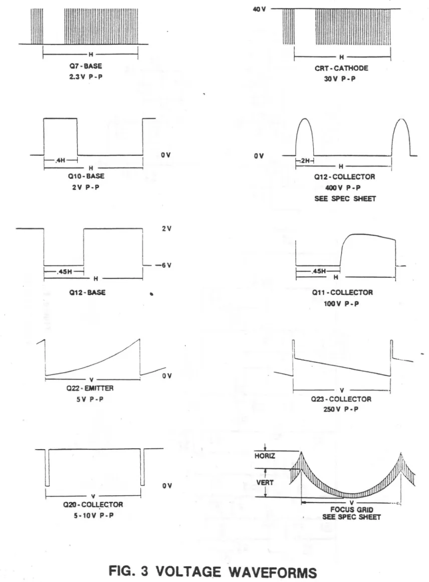
07-BASE CRT-CATHODE
2.3V Pop lOV pop
-
J
r4HJ
HI
DO DO~2H"
H!
l
Q10 -BASE 012 -COllECTOR
2V Pop 400V pop
SEE SPEC SHEET
-
l
I
~_::
I
;r--t
-
r-.4SH~
H
I
r
·
4SH~
1
.
012 - BASE .. 011 - COllECTOR
100V pop
1
II
V.v
I V - - - <
022 • EMITTER
-, I
.
--J
.
I
v~
• 5V p.p 023 . COllECTOR
2SOV pop
-t
-
1
r
·
~HOR~llll).
~
- ov
\ v
I
~~V
--c.;020 -COll.ECTOR FOCUS GRID
. SEE SPEC SHEET
5-10V Pop
FIG. 3
VOLTAGE WAVEFORMS
.
..,
.
.
,
t,"
,
.
_ 6 1t
ftnI
a.t
tN
...
I
:~
I
eJO.J.
"fJ
. ""~
.
.
Cf1 ~.
'-IV J,
L
.11"
¢
"-'" _J
violo
-_."
".;).flU
~f
,.,,,
1~
'"
..
".
'ft ....
C5 -L.
'OO"~
"
.
I
...
'Y~ 1000'"
f'9ure
Y I 0[0 "'·tPLI f I
rrt
_ J
,
....
~C~
ct
..
,,'
~L.~·rriutl
,,,.
.
..
e.o
nJ.
It
J J J
'~'b"
/ )
AQ~~--
.
•
..
Q
(5
>
~
•
I
.J
C
...
'-.l
~
N
-.i
-..
Z
CJ
--0
~
0
-I
E.
-.i
--<
-~
-0
....
>
c::
E
l
-t.:
~-.
" "
'C~
~--(
(
',
-,r"
,--•
-
~y
.~~~---~--~==================~
-
..
r\.
~
,
\.J
l/
t,.
HORIZONTAL OUTPUT
T:
A~&CX Aa'Y
---~--., ,.--~~.
'---0('
~
.
-~.-t!'--~
- - ~2
~--~~---~~---~--~~---~==~
sal'
....
T2
.Fl YBACK AaY
r""A' - - -
-~~::::::~:::::::::i:::::;~~----~~
'--...
~---~~I~--'• -.~.~~-... - .... rv
fi gure 4 .
.
FLYBACK OUiPUTS
T
\7• loY
...
,
...
..
"',
~I"'om QI'Z. ~-
R.J~"ck e~~~~V'~6~
C:,VERTi CI1L S~vT 'bOWN
,-,
'PO~ SUPPLY~i ~
t -_ _ 2_11117W_ ... _ _ . .
~
'"01 ~4.'"
l
Figure 8
"'I •
----~~
-r'-+-'-"-..
~t
0 • -~ a _ > ~:T
".[>
0G"!" .. , W \,..4_,•
o
~,
..
.....
'
• fI
.
... j: -~I:
) ~ ,-\. F -• c-'
401,~-I
ENGINEERING POLICIES
AND PROCEDURES
INDEX 1.30.009 A
_1~SS=U~E~D~A~T~E ___ ~/C2. __ ~~~~~_ APPROVED
--
-
;~/.
/' /_ ~. , ~- ::~- \ --L- ,- J... ___ //.:
MGR,. ENGINEERING / /
l!....-dJ,.--?'Z~~
\ ...
--PAGE . 1 OF 7
Subject MONOCHROME "M" SERI ES TROUBLESHOOTI NG GU I DE
1.0 SCOPE
1.1 Purpose - This standard is a guide to aid' the troubleshooting procesS----, for the "M" series product-line of Video Monitors, Inc. and is arrc)fl~
in an order that checks the simple trouble possi-bilities before proceeding with extensiVE troubleshooting. The first few checks ensure proper connection, ooeration and calibration. If the troub1p not located by these checks, the remaining steos should aid in locati the defective component. Replace defective components using the replacement instructions in VMI-STD 1.30.006 Monochrome "Mil Series Production Test Procedure, and VMI-STD 1.30.007 DHHS Production X-Radiation Test Procedure.
1.2 Applicability - This standard applies to all standard monochrome dis~ j
monitors, including end-user and OEM products, excent as may be contractually modified.
1.3 Effectivity - This standard is effective immediately on release.
1.4 Authority - The enforcement and interpretation of this standard is ir
accordance with
vm
Policy. Deviations or waivers from this standort. Ishall only be granted by the VMI Operations Manager. The interoretinq authority for this standard is the VMI Engineering Manager.
2.0
APPLICABLE DOCUMENTS
2.1 Referenced Documents
VMI-STD 1.30.006 Monochrome "W' Series Production Test Procedure ~ V~lI-STD 1.30.007 mlHS Production X-Radiation Test Procedure
2.2 Related Documents - None
3.0 GLOSSARY
Troubleshooting Guide - A step by step aid to testing a product, iSOi
fault conditions, repairing these conditions, and then calibrating it
~---~---r---r~---"-
--
."~I
~~~:
ENGINEERING POLICIES AND PROCEDURES ~ /82
Index '1.30.009 A,
SublPCT MONOCHROME "M" SERI ES TROUBLESHOOT I NG GUI DE Page 2 of 7
4.0 REQUIREMENTS
4.1 Troubleshooting Techniques
4.1.1 Check Monitor Specifications
4.1.1.1 Incorrect monitor specifications can indicate a trouble that does not
exist. If there is any question about the correct function or ooertltioFi of any monitor, see the Design Engineering Department.
4.1.2 Check Associated Equipment
4.1.2.1 Before proceeding with troubleshooting, check that the equipment used
with this monitor is operating correctly. Check that the signal is
properly connected and that the interconnecting cables are not defective. Also, check the power source;
4.1 .3 Check the calibration of this monitor, or the affected circuit if the
trouble exists in one circuit. The apparent trouble may only be
misadjustment that can be corrected by calibration. Complete calibration instructions are given in VMI-STD 1.30.006 Monochrome "M" Series
Production Test Procedure.
4. '.4 Visual .Check
4.1.4.1 Visually check the portion of the monitor in which the trouble is located.
Many troubles can be located by visual indications such as unsoldered
connections9 broken wires, damaged circuit boards, and damaged componrnts.
4.1.5 Isolate Trouble to a Circuit
4.1.S.1 Isolate trouble to a particular circuit. The symrtom often identifie~
the defective circuit. Trouble aooearing in rmre than one circuit can
indicate possible power suop1y oroblems<
4.1.6 Check Circuit Board Interconnections
4.1.6.' After the trouble has been isolated to a oarticular circuit, check fo\
loose or broken c.onnecti ons, improperly installed and/or heat damaged
components.
4.1.7 Check Voltages and Waveforms
4.1.7.1 . Often the defecti ve c;omponent can be located by checkin9 for the corni. 't.
ENGINEERING POLICIES AND PROCEDURES
!
IssueDate 4/82 Index 1.30.009
-Subject MONOC~ROME "M" SERI ES TROLJBLESHOOTI r~G GUI DE Page 3 of 7
~---~---=-4.2
4.2.1
4.2.1.1
Specific Symptoms and Remedies
SYmptom - Presence of background raster but absence of video image-This symptom indicates that the failure is in the video oortion. The presence of background raster indicates that the rest of the drive circuitry is functional. Note: Video measurements should be made by probes with short ground return leads.
Possible Problem: Video amDlifier is not biased correctly.
1. Remedy: Monitor collector of
06
with oscilloscope orobe (scale ~10 v/div @ 5 ms/div). Adjust bias control pot, P2, until video signal reaches 40 volts peak (50 volts, for units with 10 volt boost). Adjust gain control pot, Pl, until video signal range is
30 volts peak-to-peak (40 volts peak to peak for units with 10 v01~
video boos t) .
2. Remedy: If output of Q6 is correct, troubleshoot the tube socket and tube.
4.2.1.2 Possible Problem: +5 volt supply not functioning (check J8-Pin ~)
1. Remedy: Troubleshoot the raw +10 volt supply at input of +5 volt ~
regulator 15.
2. Remedy': Examine +5 volt supply line for short circuits or poor solder joints. Uote: +5 volt supply will indicate a 0 volt readihl
due to current limiting action if a short is cresent on the suoply line.
3. Remedy: Reolace +5 volt regulator ~5.
4. Remedy: Replace any active or oassive component along the supoly line that seems susoect.
4.2.1.3 Possible Problem: -5 volt supply not functioning (check J8-Pin 5). 1. Remedy: Troubleshoot -5 supply line as in section 4.2.1.2.
4.2.1.4 Possible Problem: Incorrect video input. The input video voltage rdn
shoul~ be 0.7 volts minimum and 2.5 volts maximum.
l.
2. 3.
Remedy: Check the video termination switch. The imcedance at the input of the last unit should match the imcedance of the cable Remedy: Check out video generator.
Remedy: Check Rl and R36 for proper value.
4.2.1.5 Possible Problem: Non functional input buffer - This buffer is a nann
inverting emitter follower buffer cOOlDos'ed of
04
and 015 with a gain ~ adjustment provided by Pl. When properly adjusted, the video range ~tthe emitter of Q15 should be
0.7
volts.1.
2.
3.
Remedy: Remedy: Remedy:
Check for shorts, opens, and poor solder connections visu j Check values of all passive components.
ENGINEERING POLICIES AND PROCEDURES
I
IssueDate 4 feZ Index 1.30.009 p,
I
Subject MONOCHROME "M" SERI ES TROUBLESHOOT! NG GUI DE Page.:1· of 7
4.2.1.6 (cont/d)
Possible Problem: Non-functional preamolifier - The preamplifier is
composed of Ql, Q2, and Q3 with a bias adjustment provided by bias pot, P2. The collector of Q2 should have a waveform similar to the input, amplified about 25x.
1.
Remedy: Check for shorts, opens, solder voids, etc. Measurepassive resistors. Troubleshoot 01,02, and
03.
NOTE: Voltaqemeasurements should be taken with no input siqna1 and by var'yinq the bias pot.
I
4.2.1.7 Possible Problem: Nonfunctional output stage - The output stage is a
differential amplifier cOOlpr;sed of Q7 and
QS,
with an outout transistor, Q5 and a total gain of 16. (The gain is 24 for units with the 10 volt boost video option).1. Remedy: Make sure supply voltage (+48V for standard units, +58V for units with 10 volt boost) is present at one end of R15. Make sure that there is continuity between this supoly voltage and the collector o~ Q6. (Possible 216 ohms or 432 ohms).
2. Remedy: Troubleshoot. Q6, Q7, Q8, CR4, and other suspect componerlls.
4.2.2 SymptOOl ~ Absence of background raster - This failure mode causes the
screen to become dark. Verification ot this failure mode can be made '
by turning the brightness pot, P3, clockwise until background raster ,"on
be observed. If the potentiometer hits the stop before raster appears.
this failure mode is evident.
4.2.2.1 Possible Problem: +48V supply or +HV supply not functioning - The oui·
puts of both 13 and ~4 should be +48VDC.
1. Remedy: Check fuses - 2 amp fuse of PC board and 1.5 amn fuse in Power Supply.
2. Remedy: Make sure unit is not in crowbar condition (Power down t
unit. short across CR54 temporarily, Dower unit back un, anrl chpck for correct video image).
3. Remedy: Check; nput to 030 to insure that 60 VDC is Dresent.· If ~Iot 9
t~oubleshoot the off-board power supply,
4. Remedy: Check the output of 030 (voltage level should be approx.
56 volts), An incorrect level at this point indicates a failure in one of the following components: CRSO, 030, CR5l, CR52, CR49~
R100, l3~ or l4.
5. Remedy: Check the output of l3 (voltage level should be approx. 48 VDC). An incorrect level at this Doint indicates a possible
failure in one of the following components: l3, R102,-or R101.
A resistance of less than lK ohm at the output of l3 indicates a loading of the supply. Check 011 and Q23 and other +48 V inputs.
6. Remedy: Check the output of
l4
(approx. 48 VDC). An incorrect 1~vplat this point indicates a failure in one of the followinq compoflen't,,:
ENGINEERING POLICIES AND PROCEDURES
1
I
IssueDate 4/82 Index 1.30. OOQ~
Subjf!ct MONOCHROME "M" SERI ES TROUnLESHOOTI NG GUI DE Page 5 of 7
4.2.2.2 (cont'd)
Possible Problem: ~·1issing horizontal deflection - This oroblem is
evidenced by the absence of the horizontal flyback pulse at the collector of Q12.
1. Remedy: Check l2 pin 5 for presence of horizontal oscillator pul~~
Pulses should have standard TTL signal levels and occur at the
horizontal scan rate with a duty cycle of 28-36%. Absence of ou1~,e
indicates a failure in ll, l2, or drive 5V supply. ~
2. Remedy: Check collector Qll for oroper output (see waveform guidE
at the back of the Ooerating Manual). In absence of correct signal
troubleshoot Qll, Q10, 100V suoply, +5V and -SV lines.
3. Remedy: Check collector Q12 for correct output. Possible failLlI'f
include: Flyback, Q12, CR25, CR24, and ooor connections.
4.2.2.3 Possible Problem: Absence of vertical deflection - The absence of
vertical deflection will cause the unit to enter the vertical shutdowl
mode, which has the effect of turning the screen dark. If the vertical
deflection waveform is absent from the collector of Q23, this problem ~
exists. (See waveform guide in Ooerating ~·1anual).
1.
-2.
3.
4.
Remedy: Check the outout of 021 for a r.amo waveform. If; t ; s neD..
present, troubleshoot the vertical oscillator circuit. MOTE: is01 circuit by removing Q22.
Remedy: Check for Raw +10 volt suoply at the collector of Q22.
Remedy: TroUbleshoot Q23, 022~ CR43. CR42, and Ra9.
Remedy: Check for open circuits across T1, and in .the vertical y( (
4.2.2.4 Possible Problem: Absence of +6 volt heater sUDPly
1.
2.
Remedy: Remedy:
Check continuity of tube socket, R109, CR31 ~ and CR30.
Check +10 volt raw supoly at input of ~6, CR14 and L7.
4.2.2.5 Possible Problem: Failure in vertical shutdown circuit.
1. Remedy: Check for presence of +~·8 volts at collector of Q2S. Jf
voltage is incorrect, troubleshoot Q23, 024, and 025.
4.2.2.6 Possible Problem: Absence of G2 supply voltage. NOTE: Use of high ~
voltage probe required.
1.
2.
Remedy: ChecK pin 1 of flyback connector for unfiltered G2 suoply,
voltage (1.2 KV peak). Absence of this voltage indicates flyback
failure. NOTE: Use caution and a X100 scope probe.
Remedy: Check for G2 supply voltage at red lead on PCB.
shoot CRll, P4, C34, and tube socket continuity.
Trouble-, ·
4.2.2.7 Possible Problem: Absence of l7KV supply voltage. NOTE:' Use of hioh
voltage probe required.
1. Remedy: Check second anode from flyback for prooer sUDoly vol taQf'
by inserting tip of high voltage probe between the rubber cap of i,-L\
anode lead and the CRT (See unit soecification for value of corret
voltage). Incorrect value is indicative of flyback failure. If
shi e 1 d ; s used, connect VMI second anode o'robe. CAUT! ON: VERY
ENGINEERING POLICIES AND PROCEDURES
•
l
l~~ue
Date 4/82
Subject MONOCHROME "M" SERI ES TROUBLESHOOTI NG GU I DE
.2.2.8
4.2.3
4.2.3.1
(cont'd)
Possible Problem: Bent pins on the CRT.
1. Remedy: Straighten all pins on the CRT.
Symptom - Poor Focus
Possible Problem: Misadjusted focus pots.
Index 1. 3CI.
OO~
p.,J
Page 6 0; 7
.~
J
1. Remedy: Follow adjustment orocedure ;n VMI-STD 1.30.006 Monochrol'lIt'
"M" Series Production Test Procedure to readjust focus.
4.2.3.2 Possible Problem: Failure in focus circuit.
l. Remedy: Check DC focus range of pot P5 (should be -150V to +801JV
range) .
2
.
Remedy: Check for presence of horizontal focus Darabola at base of 032.3. Remedy: Check for presence of vertical focus parabola at the emitter
4.2.4
4.2.4.1
of
Q32.
4. Remedy: Replace Q32.
Symptom ~ Insufficient, varying or excessive briqhtness.
.
Possible Problem: Poorly adjusted video bias and gain.
1. Remedy: See s~ction ~.2.1.1.
4.2.4.2 Possible Problem: Incorrect brightness suooly voltaae.
1.
2.
3.
Remedy:
If value Remedy: Remedy:
Check collector of Q25 (should be approximately 48VDC). is incorrect, see section 2.1 and 2.5 for correction. Check adjustability of pot P3.
Check tube socket continuity.
4.2.4.3 Possible PrOblem: Incorrect G2 Voltage.
,. Remedy : See section 4.2.2.6.
4.2.4.4 Possible Problem: Incorrect HV s~pply voltage.
1, Remedy: See section 4.2.2.1.
4.2.4.5 Possible Problem: Incorrect l7KV supply voltage.
1. Remedy: See section 4.2.2.7.
4.4.2.6 Possible Problem: Incorrect heater voltage (+6 volt suooly).
ENGINEERING POLICIES AND PROCEDURES
\ ,ssue
Date 4/82 Index 1.30.009 _I
•
SUbjeCT 'MONOCHRO~1E "M" SERI ES TROUBLESHOOTI NG GU I DE Page 7 01 7
4.2.4.7 (cont I d)
Possible Problem: Inoperative black clamp.
1. Remedy: For units with separate sync input, check the value of R2, and check operation of
Q5.
2.
Remedy: For units with comoosite sync, sync striDoer circuit (Collector of 05 should be +5 volt oosit;ve pulse at time of horizontal sync).Verify the correct operation of the black clarno circuit (the collector of 014 should nroduce a clampinq Dulse at the trailinq edge of the horizontal sync pulse). .
4.2.4.8 Possible Problem: Inoperative CRT
4.2.5
4.2.5.1 1.
2.
Remedy: Remedy:
Check for bent CRT socket pi·ns. Reolace CRT.
Symotom - Rolling Picture.
Possible Problem: Missing horizontal sync signal.
1. Remedy: For separate sync units, check the horizontal sync input, J8-Pin 9.
2. Remedy: For composite sync units, check the video inout for oroner~
sync wavefonn.
3. Remedy: Troubleshoot II and 17.
4.2.5.2 Possible Problem: Faulty sync strip circuit (not present on seoarate
-sync uni ts ) .
1 .
2.
Remedy: Remedy:
See section 4.2.4.7.
Troubleshoot 05 and 17.
4,2.5.3 Possible Problem: Missing vertical sync signal.
1. Remedy: For sepa rate sync un; ts. check the verti ca 1 sync i nnut, J8-Pin 10.
2. Remedy: For ccrnposi te sync uni ts, check the vi deo i nout for oroo(>\'l
vertical sync waveform. 3. Remedy: Troubleshoot 020.
4.2.5.4 Possible Problem: Faulty sync separator (not present on separate sync
l
units).
_I"-N:...=D:...=E"-X _ _ _ _ l _. 3:...;0:...;.--:.1)...:...(l.=..6 ---.:,/1__ __ __ _ _
ISSUE DATE ~-/82 PREPARED
ax,
r
'
Ii;:
APPROVEDENGINEERING POLICIES
AND PROCEDURES
PAGE l OF 21
Subject MO~!OCHRO~1E "M" SERIES PRODUCTION TEST PROCEDURE
1,0 SCOPE
1.1 Puroose - This standard establishes the Droduction test requireme~ts
for the "M" series prod;Jct-line of Video Monitors, Inc.
1.2 Applicability - This standard applies to all standard monochrome disrdi"iY
monitors, including end-user and OEM products! excent as may be contract-ually modified.
1.3 Effectivity - This sta~dard is effective inmediately on release.
1.4 Authority - The enforcements and internretation of this standard is i l:
accordance with V~I Policy. Deviations or waivers from this standarrl
shall only be granted by the vm Doerations ~'anaoer. The internretinr,
authority for this standard is-the VMI Enqineerino t1anal1er.
2.0 APPLI CJI.DLE DOCUt'Er'TS
..
2. 1 Referenced Documents
2.2
Vt1I-STD
Vt~I -STD
1. 3n. aOl
1.30.009
Related Documents
DHHS Production X-Radiation Test Procedure r1onochrOr.le lit'" Seri es Trouh1 eshoot; no r;ui de
3.0 GLOSSARY
~" 0
4.1
A. 1 • 1
4.1. 2
Test Procedure - A steD by steo aporoach to testino a nroduct, isolatij,\1
fault conditions, repairinCl tlese conditions, and then calibratinq UH
unit in order for the rroduct to achieve its specifications.
REQUI RH1ENTS
General Instructions
Power Source - Thi s product is intended to orerate fron a nower sourcc:'
that wi 11 not apply more than 250 vol ts nns between the sunn1y conduC"ill\s
or between either supply conductor and ~round.
Grounding the Product - This product is arounded throuqh the qroundina
conducto~ of the Dower cord. To avoid c~ectrical shock~ nl~Q the nowpr
cord into a nroperly wired recentacle hefore connectinn to the nroduct
jnput tenninals. A protec~;ve Clrcund connection b.v wav of the aroundi!,Q
conductor in the Dower cord is essential for safe oneration.
ENGINEERING POLICIES AND PROCEDURES
l
,ssueDate 4/82 Index 1. 311• nnf, --,
Sub)I'Cl r1OnOC::RQr1E ":i" SERIES PRODUCTIm1 TEST PPOCECURE Page 2 of 21
~" 1 . 3
4.1.4
4.1.5
4.2
4.2.1
4.2.2
(cont1
d)
Proper Fuse - To avo; d f; re hazard, use on ly the fuse of correct tyne, ~
voltage rating and current ratino as snecified in the oroduct narts li : Power-on Testing - Dangerous voltages exist at several noints in this product. To avoid personal injury, do not touch exnosed connections and components whilQ power is on. QisconnQct nower before removin~
shields, soldering, or replacing comnonents.
Special Components - This product contains comoonents that are critica with respect to increasin9 the maximum allowable radiation emissions
from the oroduct, These COmDonents are listed ocr DHIIS rules ?l-CFR Subchapter J. Uhen replacing these comnonents refer to VMI-STD 1.3n,0 .
rniHS Production X-Radiation Test Procedure. Soldering Techniques
Use ordinary 60/40 solder and a 15 watt nencil-tyne solderi~~ iron for most solderjng. Using a soldering iron with hiaher wattane-ratinn on --,
etched circuit boards can cause the etched circuit w;r;nn to sen~rate
from the board base material .
The following techniques should be used to renlace a comnonent on the circuit board. Most comnonents can be renlaced without removin~ the boards from the instruments.
1. Grip the component lead with 10n1-nose oliers. Touch solderinairlH to lead at solder connection. Do not lay iron directlv on board. ~
2. rJhen solder begins to melt, null lead out nently. This should lei; clean hole in board. If not, hole can be cleaned bv rcheatinn solder and placing sharn object (e'("J' toothnid) into the haTe to clean it out. A vacuum-type desolderina tool can also be used for this ourpose.
J. Bend lead5 of new comoonen'l to fit ho<les in board. If cor.monent replacecl while board is mouGted in instrument. cut leads so thev ~
just protrude through board. Insert leads into holes in board wit
comoonent firmly seated B9ainst board (or as nositioned oriqina'i1.\.
If i t does not seat proper'ly 5 heat sol der and aently nress comoon('~
into place.
4. Touch the iron to the connection and annly a small amount of soldr.
-to make a finn solder joint. To nrotect heat-sensitive cor.1nOrlent~"
hold the lead between the coononent body and the solder joint witl;l
pair of long-nose pliers or other heat sink.
5. Clip excess lead that orotrudes throu~h board (if not clinned in step 3).
6. Clean area around solder connection with flux-remover solvent.
ENGINEERING POLICIES AND PROCEDURES
I
IssueDate 4/£2 Inciex 1 .li,. f"):-j~, i-
I
Page 3 of 21='
Sllbif!ct ~1orwcHRm1E "M" SEPJ ES PRODllCTI ()N TESi PROC::JUP.:
~.3
~ .3. 1
4.4 4.4.1
4.4.2 4.4.3
4.4·.4
4·.4.5
Test Equipment
Preferred Test Equipment - The follo\·,inq is a listino of required test equipment Or their equivalents that is required to proncr1y test this product.
1. Tektronics 455 oscil1oscone 2 . . Data Precision 1351 OVON .
3.
Data Precision 548 frequency counter4. Data Precision V41A high voltaqe orobe
5. Variac WS~1T3 autotransfonner
6. VMI video generator
7. VHI second anode tester
Test Preparation
Check the pos i ti on of swi tches S~'!l and S\'12 on the power suon ly to enSli r e
that the switch settings match the line voltaae available to the unit.
Visually inspe~t the monitor to insure that ALL connectors are nluaqed into the proner socket and are secu~e.
Verify that all hardware on the PC board is secure.
Preadjust the potentiometers as follows:
l. 2.
.,
.J. t. 5. 6. 7. " u. 9.Adjust the Adjust the Adjus t the Mjust the Adjust the Adjust the Adj us t the Adj us t the Adjust the
G2 pot. P4, 3/4 turn clockwise.
DC focus pot~ PS, 1/~turn clockwise.
Brightness Range not, P3. counterclockwise.
Vertical Heiqht not. D10, counterclockwise. Vertical Shane pot, Pll, 3/~ turn clockwise. Vertical Lin pot, P12, l/~ turn clockwise.
High Voltage SunD1y not, P2 n, 3 turns counterclockwise. Gain pot, Pl. 1/2 turn clockwise.
Bias Dot, P2, 1/2 turn clockwise.
Connect the test equipment to the monitor as follows:
1. Connect the OVOM current meter in series between the power su()oly and the PC board.
2. Connect the hi gh voltage probe to the +Vdc receot; ca 1 of the DVOt~.
3. Connect the VHI second anode probe ;n series between the flyback
high voltage lead and the CRT. CAUTIO~: VERY HIGH VOLTAGE. It
is possible for the CRT to maintain a charqe of lO-2nKV. ExtrelTlf.' caution must be used when connecting any nrobe to the 2nd Anode of the CRT.
4. Connect the Xl DVOM probe to the +Vdc recentical of the DVOH.
ENGINEERING POLICIES AND PROCEDURES Issue
Date 11/82 Index
Sub;eCl ~1m!OCHRO~1[ "W SERI ES PRODUCTIOtJ TEST PROCEC'llD..E Page 4 of t.. .
DMM
VMI
2 f\cf
ANODE
PP..08E
to
PC
BD.
FIGURE 1
rIOTE: ~Jhile the current meter is connected to the CVOM, resistance can only be
measured with r~ference to ground. There will still be a qround loon if
the generator, power suoply and scone ground are connected.
4,4.6 (cont'd)
4.4.7
4.4.8
4.4.9
4.~. 10
Connect the A.C. power cord between th~ monitor now~r sunnlv and the
vari ac.
Set up the Vid~(1 Pa~tern Ge'1erator to qenerate the nOr.1inal video sigrl.,·
specified by the moue'l's test 5pecification.
Check the +4CV, +HV, +5V 5 -5V, and -+ 1 OV sunn 1 i es wi th the rV~1 Xl nrot.l('
for a grounded condition.
Check the continuity with the DVO~1 Xl nrobe between the chassis qrounc:
(located at the white qround return lead on the CRT brace) and the
ground screw in the lower riqht corner of the PC board.
Disconnect the flyback from
pce.
Monitor the wavefom at the collect.(,rof Qll with the scooe while slowly turnino the variac voltaoe un to ~
120 volts and back to 0 volts. The wav~fonn should be similar to
ENGINEERING POLICIES AND PROCEDURES Issue
Date . .1 / 82 inee" 1,30,006 SUbtect MONOCHROME "M" SERI ES PRODUCTI
m:
TEST PROCEDURE Page 5 of 2 '\-
... .
....
... .
....
...
•••• • ••• •••• • •••.
...
I
,....
"\. ~•
,
\
~
~
.
-
~
~
-
--
.
'.
Io·
.
. .
. ....
..
.
• • • ••• •••• '--'--L•
;
••
011 Collector
FIGURE 2
4.4.11 Attach the probe to the collector of Q23 , and reoeat 4.~.9. The waveform should be similar to Figure 3.
f
•....
• CI • •.
... .
.
.
.
. .
.
.
.
...
•••• ••••.
. .
.
....
\
•
-~
..
-
~--I ... "'
....
... ~...
~
...
•••• •••• •••• •• •• • • ••• • •••~
Q23 Collector
ENGINEERING POLICIES AND PROCEDURES
!
15sue Date 4/82 Index 1.30. f)()6 p,SubjecT r~ONOCHRm1E "W SERI ES PRODL!CTION TEST PROCEDURE Page 6 of
'-4.4.12 (cont'd)
Reconnect the flyback to the PCB. Monitor the collector of n12 with
the scope while turnino the variac up to l20V. The wavefnrm should bc~
simi lar to Figure· 4 .
...
.
•••• • • • •.
.
.
.
....
• •••..
~.
"...
.
...
.
...
I
•
~
~
.
t
f!
+
t--It
'0
t.
I
.
o~. e _ ~ • e
Co • • • • CI CI
. .
4iI • • • •.
.
....
".. ,
1
•
()12 Collector
FIGURE ~
4.5 Perfo~ance Test
4.5.1 Free Run Duty Cycle
4.5,1.1 Using a X10 probe. attach the ~SS SCODe to the collector of 011.
4.5.1.2 Adjust the voltage scale on the scope such that the waveform ranoes
from 0% to the 100% divisions.
4.5,'.3 Adjust the time scale such that the waveform completely spans the
10 time division's. See Figure S.
l
'
.
ENGINEERING POLICIES AND PROCE.,DURES
l
lssue 4/82Date IndeJ< l,30.(l1E
Subiect ~1OrWCHRm" E lOW SERI ES PRODUCT! ON TEST PROC::DURE Page 7 of {I
4.5.1.3 (cont'd)
,
•....
• ••• ••••.
...
.
...
.
~ •••• • ••• ••••
I
V
•
I
"'-~
~
t-
I
f'.:
t-
T
t-
.
.
,
.
. . ..
:
.... ....
.
...
.
...
.
...
•
•
40%
011
Coll ectorFIGURE
54.5,.1 .4 Measure the free run duty cycle at the 10% level as shown above, and
insure that it meets the monitor snecification.
4.5.2 Free Run Scan Frequency
4.5.2.1 Place the frequency counter probe at Din 5 of 72. and measure the
frequency. This frequency should fall within the monitor snecificatiulj.
4.5,3 Free Run Sweep Frequency
~.5.3. 1 Monitor the gate of 021 with the fre~uency counter and make sure that
this frequency meets the model specification.
4.5.4 q30 Emitter Voltage
4.5.4.1 Place the DVOM Xl orobe at the emitter of n30. and measure the volta9c
level. The voltage should be 56 volts: 2 volts.
4.5.5 +48 Volt Supply Volta~e
4.5.5.1 Measure the +4C volt suoply voltaqe at the output of 7.3 with the [lV~
Xl probe'. The vol tage measured shoul d be 4C volts : 2 vol ts.
4.5.6 , Flyback Supply V~ltage
ENGINEERING POLICIES AND PROCEOYRES
!
tssueDate
Subject ~10r-JOCi1Ror~E "M" SERIES PRODUCTlm: TE51 PROCEDL'RE
4.5.6.2 (cont'd)
4/82 Index
Page 8 of 2 I
Adjust the flyback sunply oot, 020, to bring the flyback SUQoly voltanr -to the level specified in the model snecification.
4.5.7 +5 Volt Supply Voltage
4.5.7.1
4.5.8
4.5
.e
.
14.5.9
t . 5.9.1
4.5.10
Measure the +~ volt supply at Din 4 of J8 with the DVOM Xl orobe. Th'i~
voltage should be +5 volts: 0.5 volts.
-5 Volt Supply Voltage
Measure the -5 volt st.:poly at Din 5 of
,w
with the DVOn Xl orobe. Thi~voltage should be -5,4 volts; 0.5 volts.
+6 Volts Supply Voltage
Measure the +6 volt supply voltaqe at the outout of 7.0 with the
['von
Xl probe. The voltage measured should be +6 vol~s ~ 0.5 volts.Tennination Switch Test. Power down the monitor.
~.5.10.1 Set the DVOM to m~asure imoedance.
~.5.10.2 Place the DVm1 Xl orobe at Din 1 of Je, and measure the innedance of the video amplifier \O:ith the video temination switch~ Sl-!l, set to "HI". The impedance measured should be greater than 201:' ohms.
4.5.10.3 Measure the impedance of the video arnn1ifier (Din 1, JA) with the
video tennination switch. Sl'il. set to "75". ihe imoedance measured -, should be 75 ohms ~ 1 oh~. .
t .5. n Vi dec 8i as ~.dj us tment
4.5.11.1 Connect the video generator to the monitor. Power up the video gene' 0 and then the video monitor.
4.5.11.2 Place the X10 orobe of trw ~55 scope on the ,iunctio~ between Pr,l arId R17, and ~onitor waveform.
4.5.11.3 Select the full white field Dattcrn from the video qenerator.
4.5.11.4 Adjust the Bias pot, P2, until the bias vo1ta ne. as measured at the reference black level is within the ranQe soecified in the model specification.
Video Gain Adjustment 4.5.12
4.5. 12'. 1 Monitor the video outDut waveform as before. Adjust the Gain oot, 01, until the video siqnal sw;nq meets the ranne sneci'fied in the model -;
soecification.
ENGINEERING POLICIES AND PROCEDURES
!
Date IS;U€ l/2.2Index 1 .30.006
Sub/f'ct r10NOCHRm1E "M" SERIES PRODUCTIOt: TEST PROCEDURE Page 9 of 21
4.5.13 (cont'd)
Black level Stability
4.5.13.1 Monitor the video output waveform as before. Switch the video invert switch on the video generator alternatively on and off, and measure the va ltage sh i ft of the black 1 eve 1 of the vi deo amn 1 i fi er outout wavefoYiil. This d.c. shift must be less than or equal to 1 volt.
4.5.14 Remote Contrast Test (For units with the remote contrast ootion only)
4.5.1~·.1 Monitor the video output as before. Connect the remote contrast
potenti ometer. Adj us t the poten ti aneter, and observe the change in 1..I1(
vi deo output waveform. Turni ng the remote contras t potenti ometcr fr0!l1 maximum to minimum should decrease the ranae of the video outnut, but
the reference black level should not change by more than 1.0 volts d.c.
4.5.14.2 Remove the remote contrast pot before nroceedin9.
4.5.15 Brightness Suon1y VoltaQe
4.15.1 Measure the ~rightness supply voltaoe at pin
e
ofJe
with the DVOM, ensuring that this voltaae is -130 volts! 20 volts.4.5.16 G2 Setting
4.5.16.1 Place the DVOM high voltage orobe on the red lead wire of the tube
socket, J9, and monitor the yoltage level. CAUTIml: HIGH VOLTAGE
MAY GE PRESENT.
4.5.16.2 Adjust the G2 pot, P4, until the G2 voltaoe is at the level snecified in the model specification.
4.5.17 Brightness Setting
4.5.17.1 Switch the video invert switch of the video generator to select a full black field. Observe the faceolate of the monitor, and adj~st the Gl
pot~ P3t until the background raster is just short of be;nq visible ..
4.5.18 Video Shutdown
4.5,18.1 Switch the video inout switch of the video generator to select a full white display.
4.5.18.2 Ground the bas·e of Q23 with a jumper wire.
4.S.1L.3 If the video shutdown circuit is operating correctly, the monitor's display should be shut off comoletely.
4.5.19 Horizontal Delay Range
ENGINEERING POLICIES AND PROCEQURES
I
I ssueDate 4/82 Index 1.30.n06 f;.
~10NOCliROt'1E "M" SERIES PRODUCTIOt' TEST PROCEDURE Page 10 of 2 i
4.5.19.2 (cont'd)
Adjust the Horizontal Delay Dot, P6. to measure the negative-going Dulse width.
within the range specified in the model
the maximum Dossib1e delay. 01;
This pulse width should be snec·ification.
4.5.19.3 Adjust the Horizontal Delay pot to the minimum possible delay and measure the negative-going pulse width. This Dulse width should be within the range specified in the model IS speclficat;on.
4.5.20 Locked-In Duty Cycle
4.5.20.1 Using a X10 probe. attach the ~55 SCODe to the collector of 011.
4.5.20.2 Adjust the voltage scale on the scope such that the waveform ranoes fYulr
the O~ to the 100% divisions.
4.5.20<3 Adjust the time scale such that the waveform comnletely snans the 10 time division's. See Figure 6.
4<5.20.4 Measure the locked-in duty cycle at the lO~ level as shown in Fiaure G
and insure that it meets the monitor snecifications .
.
-11...
.
.
... .
~...
eol--~--~-r--+-~~~~~~~~--~-1
I
N~
~
... ,...-I ...
~t't e _ • • • • • • • • • • • • • • • • • • c • • •1
Ql1 Collector
FIGURE 6
-ENGINEERING POLICIES AND PRO~EDURES
J
IHueDate
MOtlOCHRm·1E "M" $ER I ES PRODUCTI O~i TEST P ROCE~URE
4.5.21 (cont'd)
Linearity and Pincushioning Adjustments
4/82 Index 1.30.005
Page 11 of 21
4.5.21.1 Select the linearity slide set up for the specified picture size, and
place it into the slide projector.'
4.5.21.2 Adjust the height of the projector such that the center of the lens 1S
at the same height as the center of the monitor's CRT.
4.5.21.3 Adjust the distance between the projector and the monitor such that thE:
outside rows of donuts projected on the CRT phosohor are at the size
specified in the model specification.
4.5.21.4 Adjust the projector orientation with respect to the monitor such thai the