Available Online at www.ijpret.com 222
INTERNATIONAL JOURNAL OF PURE AND
APPLIED RESEARCH IN ENGINEERING AND
TECHNOLOGY
A PATH FOR HORIZING YOUR INNOVATIVE WORK
DESIGN OF QUATERNARY ADDER FOR HIGH SPEED APPLICATIONS
MS. PRITI S. KAPSE1, DR. S. L. HARIDAS2
1. Student, M. Tech. Department of Electronics (VLSI), GHRACET, Nagpur, India. 2. H.O.D. of Electronics and communication (VLSI), GHRACET, Nagpur, India.
Accepted Date: 05/03/2015; Published Date: 01/05/2015
\
Abstract: Routing has become the main contributor in many areas of design such as area, delay and power. Multiple Valued Logic (MVL) offers a means to reduce the routing since each wire in MVL can carry the twice as much information as single binary wire. Reducing this routing directly leads to the reduction of overall circuit area and power consumption. Rapid advancement in VLSI technology makes it possible to couple several binary inputs to form a multivalued input for faster processing. In this paper, we present the Quaternary Signed Digit number (QSD) system which comes under the Multiple Valued Logic (MVL); to achieve fast processing by achieving the carry free arithmetic operations. This approach can greatly enhance the performance of digital signal processing (DSP) system.
Keywords: Signed Digit Number, Digital Signal Processing, Multiple Valued Logic
Corresponding Author: MS. PRITI S. KAPSE
Access Online On:
www.ijpret.com
How to Cite This Article:
Available Online at www.ijpret.com 223 INTRODUCTION
For many years digital devices have been designed using binary logic. Even today also, the latest computing systems are designed and developed using binary logic only. Then why there is a need of inventing multi valued logic over binary logic??? With the advancing technology, interconnections are the main contributor for delay, area and power consumption. One of the solution for the problem of interconnection is that: what if we will develop the idea of transmitting the number of logic levels through a single wire. Since, multi valued logic scheme allows more data to be grouped in single digit, researchers seems the use of multivalued logic as a solution for the above problem.so, researchers have been working on the idea of using multivalued logic for many years. Existing VLSI technology has put some limitations on the selection of number of logic states, therefore researchers seems the use of Quaternary logic systems to be best in this regards. The paper is organized as follows: In this paper we review some work related to QSD number system. Section2 explains basic concept of performing any operation in QSD number system. Section3 explains quaternary signed digit number system. Section4 explains converter of decimal to Quaternary Signed Digit number.Section5 explains converter of QSD number to decimal number. Section6 explains QSD added. Conclusion of paper is given in Section7.
Available Online at www.ijpret.com 224 II. QUATERNARY SIGNED DIGIT NUMBERS
Quaternary is the base four numeral system which uses the digits 0,1,2 and 3 to represent any real number. QSD numbers are represented with the digit set from -3 to +3 i.e. with {3̅, 2̅, 1̅, 0, 1, 2, 3 }. 3̅, 2̅, 1̅, represents the signed numbers -3, -2, -1 respectively. Signed digit numbers have redundancy associated with it therefore quaternary is also called as base-4 redundant number system. Degree of redundancy increases with increase of radix[6]; therefore higher radix number systems usually have higher redundancy.
Redundancy allows multiple representation of any integer quantity i.e.610= 12𝑄𝑆𝐷= 22̅𝑄𝑆𝐷 . In QSD, numbers are represented using 3 bit 2’s complement notation. In general decimal signed digit number (D)can be represented in terms of quaternary signed digit number (Q) as follows;
D = ∑ 𝑋𝑖 𝑖 . 4𝑖
Where; 𝑋𝑖 can be any value or digit from the digit set {3̅, 2̅, 1̅, 0, 1, 2, 3 }for achieving the appropriate decimal representation. In this number system; a QSD negative number is nothing but the QSD complement of the QSD positive number [7], i.e. 3̅’ = 3 ; 3’ = 3̅; 2̅’ = 2 ; 2’ = 2̅ ; 1̅’ = 1 ; 1’ = 1̅.For eg.23310 = 332̅1𝑄𝑆𝐷 and −23310= 3̅ 3̅21̅𝑄𝑆𝐷 . In QSD single decimal number can be represented in multiple ways. Operation on large number of digits such as 64, 128, or more can be implemented with constant delay and complexity. A high speed and area effective adders and multipliers can be implemented using QSD number system.
III.BASIC CONCEPT:
Available Online at www.ijpret.com 225 IV. DECIMAL NUMBER TO QSD NUMBER CONVERTER:
As mentioned before; for any operation to get performed in QSD, we have to first convert the binary or any other input into quaternary signed digit (QSD) number. Now, we will go through some ideas related to the conversion of decimal number to QSD number[1]. For this purpose we exploit some fundamentals as they plays an important role in corresponding algorithm.As the numbers can be positive and can also be negative. In digital system, positive numbers are called as unsigned numbers whereas the negative numbers are called as signed numbers.
Available Online at www.ijpret.com 226 quaternary signed digit number whether the decimal input is positive or negative number. If the given input decimal number is positive then we will get a QSD number at the output in which each digit will be positive. This QSD output is represented with 3 bit 2’s complement notation in simulation result. If the given input decimal number is negative, then after conversion we will get the corresponding QSD number at the output in which each digit will be negative. This QSD output can also be represented in 3 bit 2’s complement notation in simulation result.
The conversion of a decimal number into corresponding QSD number can be performed by modulo-4 arithmetic, in which the given decimal number is successively divided by 4 and by keeping the track of the remainders. This process continues until the quotient becomes zero. When we divide the given decimal number by 4, the quotient which we get is nothing but the just another QSD number and remainder is nothing but the digit 𝑞𝑠𝑑0i.e. (LSB) least significant bit of our output QSD number. Further dividing the quotient by 4 gives the new quotient and the remainder which is the next digit i.e. 𝑞𝑠𝑑1. Continuing the process of dividing the new quotient by 4; determining the remainder (one digit) in each step will produce all digits of the QSD integer, and this process continues until quotient becomes zero. It is important to note that; the least significant bit (LSB) is generated first and most significant bit (MSB) is generated last. We can say that; collection of remainders forms the collection of QSD digits which in terms forms the resultant QSD number.
Available Online at www.ijpret.com 227 given input decimal number is positive and binary number indicates unsigned number. It is important to note that; “0” is neither positive nor negative hence if decimal input is 0 in the form of binary then output will always be 0. Decimal number that can be represented with 4-bits , 8-4-bits , 16-4-bits etc. in 2’s complement binary form are -8 to +7 , -128 to +127 , -32768 to +32767 etc. respectively. Operation on these large numbers are performed with constant delay and less complexity in QSD number system.
V. QUATERNARY TO DECIMAL NUMBER CONVERTER:
Any n-digit QSD number can be converted into its equivalent decimal number by using the following equation;
D = ∑𝑛−1𝑖=0 𝑋𝑖 . 4𝑖
Where; 𝑋𝑖 can be any value or digit from the digit set {3̅, 2̅, 1̅, 0, 1, 2, 3 } for achieving the appropriate decimal representation. For required decimal representation, each digit in the QSD number is multiplied by its quaternary weight. In general QSD integer is expressed by; QSD = 𝑞𝑠𝑑𝑛−1 𝑞𝑠𝑑𝑛−2𝑞𝑠𝑑𝑛−3 ……… 𝑞𝑠𝑑1𝑞𝑠𝑑0 which represents the equivalent decimal value as; D (QSD) =𝑞𝑠𝑑𝑛−1 × 4𝑛−1 + 𝑞𝑠𝑑𝑛−2 × 4𝑛−2 + ……… + 𝑞𝑠𝑑1× 41 + 𝑞𝑠𝑑0× 40. In this way QSD number
is converted into its equivalent decimal number by using above equation. Some examples are;
102̅1𝑄𝑆𝐷 = 1 × 43 + 0 × 42 + 2̅ × 41 + 1 × 40
= 64 + 0 – 8 + 1
= (57)10
1̅0̅21̅𝑄𝑆𝐷 = (−57)10
VI. QSD ADDER:
Available Online at www.ijpret.com 228 There are two steps involved in carry free addition;
STEP 1: Generates an intermediate carry and sum from the QSD input i.e. from addend and augend.
STEP 2: Combines the intermediate sum of current digit with the carry of the lower significant digit.
To prevent carry from further rippling two rules are define;
RULE 1: States that the magnitude of intermediate sum must be less than or equal to 2 or it must not be greater than 2.
RULE 2: States that the magnitude of intermediate carry must be less than or equal to1 or it must not be greater than 1.
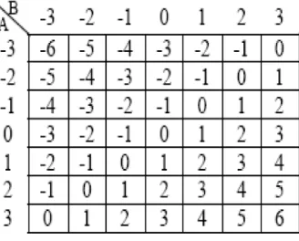
Consequently the magnitude of second step output cannot be greater than 3, which can be represented by a single digit QSD number hence no further carry is required. Outputs of all possible combinations of QSD inputs i.e addend and augend are shown in table 1.
Table 1
We can see that output ranges from -6 to +6 and these output values can be represented in QSD format as shown in table 2.
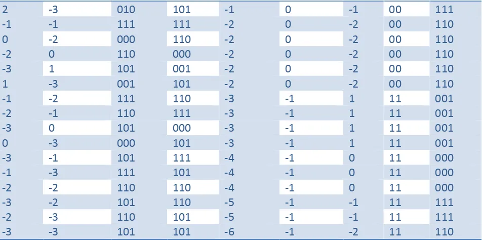
Available Online at www.ijpret.com 229 intermediate carry bit. This intermediate carry propagates from lower significant digit to higher significant digit position and to prevent this propagation QSD number representation is used[9]. QSD number has redundancy associated with it in which same decimal number can be represented in more than two QSD representations. But we chose only those QSD coded number which meet our defined rules(as shown in table2) to prevent the further rippeltion of carry.
Table 2
THE INTERMEDIATE CARRY AND SUM BETWEEN -6 TO 6 :
To prevent carry propagation, these two digits i.e. 𝑛𝑡ℎ intermediate sum and 𝑛 − 1𝑡ℎ intermediate carry bits should never form the pair (3,3) (3,2) (3,1) (3̅, 3̅) (3̅, 2̅) (3̅, 1̅) . In this way,
when intermediate sum and intermediate carry go up to maximum value of 2 and 1 respectively, final result of operation will become carry free. Mapping between the 3-bit 2’s complement inputs (addend and augend) and outputs (intermediate carry and sum) are shown in binary format in table 3. Intermediate carry ranges between -1 to +1 and can be represented
with 2 bit binary number but we have taken the 3-bit representation of carry bit for bit compatibility. Outputs of all possible combinations of intermediate sum and intermediate carry
Available Online at www.ijpret.com 230 Table 3
INPUT OUTPUT
QSD Binary Dec QSD Binary
Imal
Ai Bi Ai Bi Su Ci Si Ci Si
M
3 3 011 011 6 1 2 01 010
3 2 011 010 5 1 1 01 001
2 3 010 011 5 1 1 01 001
3 1 011 001 4 1 0 01 000
1 3 001 011 4 1 0 01 000
2 2 010 010 4 1 0 01 000
1 2 001 010 3 1 -1 01 111
2 1 010 001 3 1 -1 01 111
3 0 011 000 3 1 -1 01 111
0 3 000 011 3 1 -1 01 111
1 1 001 001 2 0 2 00 010
0 2 000 010 2 0 2 00 010
2 0 010 000 2 0 2 00 010
3 -1 011 111 2 0 2 00 010
-1 3 111 011 2 0 2 00 010
0 1 000 001 1 0 1 00 001
1 0 001 000 1 0 1 00 001
2 -1 010 111 1 0 1 00 001
-1 2 111 010 1 0 1 00 001
3 -2 011 110 1 0 1 00 001
-2 3 110 011 1 0 1 00 001
0 0 000 000 0 0 0 00 000
1 -1 001 111 0 0 0 00 000
-1 1 111 001 0 0 0 00 000
2 -2 010 110 0 0 0 00 000
-2 2 11 010 0 0 0 00 000
-3 3 101 011 0 0 0 00 000
3 -3 011 101 0 0 0 00 000
0 -1 000 111 -1 0 -1 00 111
-1 0 111 000 -1 0 -1 00 111
-2 1 110 001 -1 0 -1 00 111
1 -2 001 110 -1 0 -1 00 111
Available Online at www.ijpret.com 231
2 -3 010 101 -1 0 -1 00 111
-1 -1 111 111 -2 0 -2 00 110
0 -2 000 110 -2 0 -2 00 110
-2 0 110 000 -2 0 -2 00 110
-3 1 101 001 -2 0 -2 00 110
1 -3 001 101 -2 0 -2 00 110
-1 -2 111 110 -3 -1 1 11 001
-2 -1 110 111 -3 -1 1 11 001
-3 0 101 000 -3 -1 1 11 001
0 -3 000 101 -3 -1 1 11 001
-3 -1 101 111 -4 -1 0 11 000
-1 -3 111 101 -4 -1 0 11 000
-2 -2 110 110 -4 -1 0 11 000
-3 -2 101 110 -5 -1 -1 11 111
-2 -3 110 101 -5 -1 -1 11 111
-3 -3 101 101 -6 -1 -2 11 110
Table 4
We have taken the input range according to our defined rules and hence our output ranges from +3 to -3 and which can be represented by a single digit QSD number hence no further carry is required. Addition operation for higher order digit does not wait for the completion of addition operation of immediate lower order digit resulting in parallel addition of each individual pair of digits.
MVL: Multiple valued logic (MVL)
Available Online at www.ijpret.com 232 interconnections. Reducing interconnection directly reduces overall power consumption and circuit area. Development in novel electronic devices and optical devices makes it possible to implement circuits for complicated logic system. Many of such complicated systems are able to deal with more than two logic state, so if we use multiple valued logic for the design of digital circuit their efficiency could be utilized in better way. In binary logic, device size is reduced by reducing transistor size but transistor size cannot be reduced indefinitely. By using MVL number of transistors can be reduced greatly. Therefore we can say that multivalued logic is a best solution for the increasing data storage demand and faster computation.
In binary logic, the size of the device is reduced by reducing the size of the transistor. But it has a limit, since the size of transistor cannot be reduced indefinitely. By applying multi-valued logic to the design, word lengths and the number of transistors can be greatly reduced.
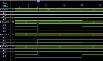
Fig. Simulation results for Quaternary adder.
VII. CONCLUSION:
This review paper discussed the idea of both converters; decimal number to QSD number converter and also QSD number to decimal number converter. By using this higher radix number system such as QSD we can perform the operations on large number of bits with constant delay and less complexity. As technologies are becoming more complex, multivalued logic (MVL) will be the future of circuit design. Hence MVL logic scheme can be a solution for the demand of increasing data storage capability and faster processing.
REFERENCES:
Available Online at www.ijpret.com 233 2. Reena Rani, Neelam Sharma, L.K.Singh, “FPGA Implementation of Fast Adders using Quaternary Signed Digit Number System” IEEE proceedings of International Conference on Emerging Trends in Electronic and Photonic Devices & Systems (ELECTRO-2009), pp 132-135, 2009.
3. O. Ishizuka, A. Ohta, K. Tannno, Z. Tang, D. Handoko, “VLSI design of a quaternary multiplier
with direct generation of partial products,” Proceedings of the 27th International Symposium
on Multiple-Valued Logic, pp. 169-174, 1997.
4. Behrooz Parhami, “Carry-Free Addition of Recoded Binary Signed- Digit Numbers”, IEEE Transactions on Computers, Vol. 37, No. 11, pp. 1470-1476, November 1988.
5. Ricardo Cunha, “quaternary lookup tables using voltage mode CMOS logic design”, ISMVL 2007, 37th International Symposium on Multiple- Valued Logic, pp.56-56, 2007, 13-16 May, 2007.
6. Vasundara Patel K S, K S Gurumurthy, “Design of High Performance Quaternary Adders”, International Journal of Computer Theory and Engineering, Vol.2, No.6, pp. 944-952, December, 2010.
7. Behroozperhami “generalized signed digit number systems, a unifying frame work for redundant number representation “.IEEE transactions on computers, vol 39, no.1, pp.89-98,January 19990.
8. Reena Rani, Neelam Sharma, L. K. Singh, “Fast Computing using Signed Digit Number System” IEEE proceedings of International Conference on Control, Automation, Communication And Energy Conservation -2009, 4th-6th June 2009.