Physics and Astronomy Publications
Physics and Astronomy
9-1996
Photoelectron spectra of an Al70Pd21Mn9
quasicrystal and the cubic alloy Al60Pd25Mn15
Cynthia J. Jenks
Iowa State University, cjenks@ameslab.gov
S.-L. Chang
Iowa State UniversityJames W. Anderegg
Iowa State University, anderegg@ameslab.gov
Patricia A. Thiel
Iowa State University, thiel@ameslab.gov
David W. Lynch
Iowa State University, dlynch@iastate.edu
Follow this and additional works at:
http://lib.dr.iastate.edu/physastro_pubs
Part of the
Atomic, Molecular and Optical Physics Commons
, and the
Condensed Matter
Physics Commons
The complete bibliographic information for this item can be found athttp://lib.dr.iastate.edu/physastro_pubs/96. For information on how to cite this item, please visithttp://lib.dr.iastate.edu/howtocite.html.
Photoelectron spectra of an Al70Pd21Mn9 quasicrystal and the cubic
alloy Al60Pd25Mn15
Abstract
Photoelectron spectra of a fivefold quasicrystalline alloy Al70Pd21Mn9 and a related cubic alloy
Al60Pd25Mn15 reveal two noteworthy features. The first is that the Pd 3d lines fall at binding energies which
are 2.2 eV higher than in pure Pd. A similar shift is observed for Pd in other alloys. The second noteworthy
feature is that the Mn 2p32 line is very sharp in the quasicrystal. Fitting the experimental peaks with a
Doniach-Sunjic line shpae suggests that the position and density of Mn states near EF is very sensitive to the
structural and/or chemical environment of Mn in the alloys, and that this accounts for the shape of the 2p32
Mn line. The sharpness of the Mn line may be a fingerprint of the quasicrystalline phase within the AlPdMn
family.
Keywords
Ames Laboratory, quasicrystalline, Doniach-Sunjic
Disciplines
Atomic, Molecular and Optical Physics | Condensed Matter Physics | Physics
Comments
This article is from
Physical Review B
54 (1996): 6301, doi:
10.1103/PhysRevB.54.6301
. Posted with
permission.
Photoelectron spectra of an Al
70Pd
21Mn
9quasicrystal and the cubic alloy Al
60Pd
25Mn
15C. J. Jenks, S.-L. Chang, J. W. Anderegg, P. A. Thiel, and D. W. Lynch
Departments of Physics and Chemistry and Ames Laboratory, Iowa State University, Ames, Iowa 50011
~Received 13 February 1996!
Photoelectron spectra of a fivefold quasicrystalline alloy Al70Pd21Mn9 and a related cubic alloy Al60Pd25Mn15reveal two noteworthy features. The first is that the Pd 3d lines fall at binding energies which are 2.2 eV higher than in pure Pd. A similar shift is observed for Pd in other alloys. The second noteworthy feature is that the Mn 2 p3/2 line is very sharp in the quasicrystal. Fitting the experimental peaks with a Doniach-Sunjic line shape suggests that the position and density of Mn states near EFis very sensitive to the structural and/or chemical environment of Mn in the alloys, and that this accounts for the shape of the 2 p3/2 Mn line. The sharpness of the Mn line may be a fingerprint of the quasicrystalline phase within the AlPdMn family.@S0163-1829~96!06232-7#
I. INTRODUCTION
Quasicrystalline films1–7 can have properties which ren-der them useful. These properties include attractive tribologi-cal characteristics, and apparent oxidation resistance.8–14The fact that such properties are controlled mainly by surface and interface phenomena provides an impetus to examine these phenomena on an atomic scale.
A primary, common method of surface analysis is x-ray photoelectron spectroscopy~XPS!. The main purpose of this paper is to analyze the peak positions and shapes of the spec-tra obtained with XPS, for a clean, fivefold surface of AlPdMn. Such an analysis can shed light upon the electronic properties of the material, particularly when compared with the spectra of related crystalline materials. The material which is the primary focus of our study is a ternary quasic-rystal alloy, Al70Pd21Mn9. The materials we choose for com-parison are a cubic AlPdMn alloy with a composition similar to the quasicrystal, and samples of the pure metal constitu-ents Al, Pd, and Mn.
A few basic facts regarding the electronic structure of the quasicrystalline ~icosahedral! alloy are known already. The quasicrystal is metallic, but the density of states is low at the Fermi energy EF.15,16A ‘‘pseudogap’’ at the Fermi edge is mentioned frequently.17–22 Consequently, the alloy exhibits high electrical resistivity.16,23,24 The crystalline, cubic alloy Al60Pd25Mn15, is also a poor conductor.25This stands in con-trast to the constituent metals. Aluminum is a nearly free-electron metal with a moderate density of states at the Fermi level, while Pd and Mn are transition metals with larger den-sities of states at the Fermi level.
Further detail on the electronic structure of the AlPdMn quasicrystal is available from various photoelectron and x-ray-absorption techniques which probe the valence bands,21,22,26 and from electronic structure calculations.27 These show that the Mn 3d states are located near, and on both sides of, EF hybridized with Al valence states. The Pd 4d states lie several eV below EF. A corresponding level of information is unavailable for the cubic alloy.
II. EXPERIMENTAL DETAILS
The quasicrystal sample used in our studies is a single grain in the shape of a flat wafer, approximately 33631 mm3in size, cut with a fivefold axis normal to the surface. It is mechanically polished to a mirror finish with 1mdiamond paste. The response of the fivefold Al70Pd21Mn9 surface to treatment in vacuum, and to oxidizing environments, is known.28,29The sample is cleaned by cycles of ion bombard-ment and vacuum anneals at temperatures of 870 K. This treatment yields a high-quality fivefold pattern in low-energy electron diffraction, and a surface composition close to that of the bulk.30A Pd-rich secondary phase is present at a level of 0.7% by volume, based upon examination with scanning electron and scanning Auger microscopies.29
The sample of the cubic alloy has nominal bulk composi-tion Al60Pd25Mn15, and has a surface composition— measured with XPS after ion bombarding, annealing to 870 K and recooling to room temperature—of Al5661Pd3662Mn861.30The sample is a single crystal, with a structure of the B2 space group~CsCl structure!, determined experimentally by x-ray diffraction, and with a lattice con-stant 3.02 Å. The sample is roughly 153631 mm3 in size. Its surface happens to be oriented 9.5° from the ~111!, 29° from the ~110!, and 48° from the ~100!. Its Van der Pauw resistivity at room temperature is 0.13260.001 mVcm.25 It is ferromagnetic with a Curie temperature of 2150 °C,31 well below the temperature at which our measurements are made. Both the quasicrystal and the cubic alloy are grown at the Materials Preparation Center of the Ames Laboratory, by Dr. T. Lograsso and D. Delaney. No secondary phases can be detected with scanning electron and scanning Auger microscopies.29
In addition to the AlPdMn samples, three pure samples of metallic Al, Pd, and Mn are used. Their preparations are described in another paper.29For each of these three metals, we compare photoelectron spectra of the metals present in the alloy quasicrystal, with the spectra they exhibit as pure
~elemental! samples. By making these measurements in house, we avoid problems which could arise by citing data for the pure metals available in the literature, since literature
PHYSICAL REVIEW B VOLUME 54, NUMBER 9 1 SEPTEMBER 1996-I
54
values would be generated in a variety of laboratories using a variety of instrumentation and cleaning procedures.
The photoelectron data are acquired using a Perkin-Elmer Multitechnique Chamber, Model 5500, and withPHI-ACCESS
software. The base pressure of the chamber is 3310210Torr or better. The x-ray source provides monochromatized Al
Karadiation at a power of 250 W. The takeoff angle used in these experiments is 45°. Binding energies are calibrated against two different samples, Au~using the 4 f7/2 photoelec-trons at 84.0 eV!and Cu ~using the 2 p3/2 photoelectrons at
932.7 eV!. The measured resolution is 0.65 eV, for a 29.5-eV pass energy, and for the 3d5/2 electrons of Ag. All photo-emission spectra are recorded at room temperature.
III. PHOTOELECTRON SPECTRA AND DISCUSSION
The photoelectron spectra are compiled in Fig. 1, while the widths and positions of the core-level peaks are specified in Table I. The core-level spectra of the two alloys depend upon the conditions of their preparation. This is shown for the quasicrystal by comparison of the top two rows of Fig. 1. The top row@panels~a!–~c!#shows spectra obtained after ion bombarding the quasicrystal at room temperature, and the second row @panels ~d!–~f!# shows spectra after treatment
[image:4.612.62.289.60.291.2]~vacuum annealing, or ion bombardment!at 870 K. Figure 1 and Table I show that the Al and Pd peaks are nearly iden-tical in shape and location after these two treatments, but that the Mn peaks are much sharper after high-temperature treat-ment. This may be related to the fact that ion bombardment at room temperature perturbs the surface composition, pre-sumably via preferential sputtering, leaving the surface highly enriched in Pd.28,30Such a surface is also structurally perturbed, since it does not yield a fivefold pattern in low-energy electron diffraction ~LEED!.28 ~Structural perturba-tion by ion bombardment, leading to damping or extincperturba-tion of the characteristic LEED pattern, is well known for single crystals.! Either of these perturbations—chemical or structural—could be responsible for the difference in line shapes between Figs. 1~c!and 1~f!. However, it is interesting to note that our data show that line shapes and linewidths in pure Mn do not depend at all upon whether the sample is sputtered at room temperature or annealed. The spectrum shown in Fig. 1~l!is of pure, clean, annealed Mn; the spec-trum of the sputtered, unannealed surface is not shown, but it exhibits precisely the same shape and width. This may sug-gest that chemical effects are more important than structural ones in causing variations in the Mn peak shape. The cubic alloy behaves in a fashion which is qualitatively similar to the quasicrystal, undergoing strong Pd enrichment during ion bombardment at room temperature, and exhibiting a much
FIG. 1. XPS spectra for Al, Pd, and Mn core levels. The top row of panels shows results from the quasicrystal surface after ion bom-bardment at room temperature, without annealing. The second panel shows results after ion bombardment, or after annealing in vacuum, at 870 K. The third panel shows data for the cubic alloy, annealed at 870 K. The bottom row shows results for the pure metals, annealed at 810–870 K. The vertical lines mark the peak positions of the pure metals, to facilitate comparisons.
TABLE I. Positions~binding energies, E0!and full widths at half maximum~FWHM!of the XPS peaks. Both quantities are in units of eV. Values are extracted from data such as those shown in Fig. 1.
Sample
Al 2 p Pd 3d Mn 2 p
1/2 3/2 5/2 1/2 3/2
E0 FWHM E0 FWHM E0 FWHM E0 FWHM E0 FWHM
Quasicrystal sputtered at 300 K
@Figs. 1~a!–1~c!#
73.1 1.05 342.2 0.95 337.0 0.93 649.5 1.92 638.4 2.31
Quasicrystal sputtered at 870 K
@Figs. 1~d!–1~f!#
73.0 1.04 342.6 1.00 337.3 1.01 649.5 1.74 638.5 1.01
Cubic alloy
annealed at 870 K
@Figs. 1~g!–1~i!#
73.1 1.07 342.4 0.90 337.1 0.91 649.6 2.28 638.5 1.83
Pure metal
annealed T.800 K
@Figs. 1~j!–1~l!#
72.9 0.96 340.4 1.21 335.1 1.13 650.0 2.22 638.8 1.69
broader Mn peak after preparation in this manner than that obtained after annealing.
The second and third rows of Fig. 1 and Table I show the data for the clean, annealed quasicrystal surface and for the clean, annealed crystalline surface. It can be seen that the Al and Pd features are virtually identical in shape and position, whereas the Mn peak, especially the 3/2 component at 638.4–638.8 eV, is significantly broader in the crystalline phase.
Turning now to a comparison between the two alloys and their pure metal constituents, the fourth row of Fig. 1 shows XPS spectra for the pure elemental components after anneal-ing. Comparing the second and third rows ~the annealed al-loys!with the fourth row~the annealed, pure metals!shows that the Al peaks are almost unchanged in both shape and position, upon going from the alloys to the pure metal. The other two metals, Pd and Mn, show significant differences, however, when analogous comparisons are made. Most strik-ing are the difference in peak position for Pd, and the differ-ence in peak shapes and widths—especially in the 3/2 peak—for Mn. We will discuss the peak position for Pd first. For pure Pd, our measured values of the peak position, or binding energy E0, are 340.4 and 335.1 eV, for the 3/2 and 5/2 components, respectively. The latter number agrees closely with literature values, which are 335.2 eV for the bulk component measured on a 110 face of Pd~Ref. 32!and 335 eV for the bulk component measured on a 100 face.33 The shifts for the Pd core levels in the alloys, relative to the pure metals—2.2 eV higher in the quasicrystal and 2.0 eV higher in the cubic alloy—are large, but Pd core-level shifts tend to be large upon alloying.34,35The observed shifts are very close to the 2.15 eV found for Pd in dilute solution in Al which might be expected to resemble these alloys.
It is known that E0can differ between a metal in its pure form, and a metal contained in an alloy or compound, due to differences in local charge environment or oxidation state
~initial-state effect!,36,37 or photohole screening ~final-state effect!,38 or both.39 The shift in the dilute alloy Pd-Al has been explained34with a commonly used model in which the core-level peaks in all metallic samples arise from a final state that is fully screened, which allows the final-state core-ionized charge distribution to be replaced by that of the ground state of the next element in the periodic chart—the
Z11 approximation.40,41This analysis is more complicated in the case of concentrated alloys and intermetallic com-pounds, and even more so for ternary alloys. Andersen
et al.42have measured the shift of the Pd 3d core level at the surface on Pd~111! and Pd~110! ~shifts with respect to the bulk Pd core level!and carried out ab initio calculations of these shifts. In this case, final-state effects were found to be important, contributing about 0.1 eV to the surface core-level shift, while the initial-state shift was about 0.5 eV. The Z11 approximation was found to produce errors of about 0.1 eV in the surface shift from the neglect of relaxation. Since the screening of the 3d hole was different on the surface than in the bulk, both initial- and final-state effects are also probably important for the Pd 3d XPS binding energy in alloys and compounds.
The peak shape for Mn is the second obvious variable in Fig. 1 and Table I. The 2 p3/2peak is very sharp in the qua-sicrystal, wider in pure Mn, and widest in the cubic alloy.
Inspection of Fig. 1 indicates that the sharpness in the qua-sicrystal is due, at least partly, to a reduction in intensity of the high-energy tail. The origin of this effect is clarified somewhat by curve-fitting results, discussed below.
Fitting the shapes of the Pd and Mn peaks in the alloys and in the pure metals allows extraction of information which is more quantitative.~We do not attempt to fit the Al peaks, since the 2 p1/2 and 2 p3/2 contributions are unre-solved.!For a metal, the line shape is usually of the Doniach-Sunjic form,43,44which is a closed form of the convolution of a Lorentzian, whose width represents the core-hole lifetime, and a spectrum with a one-sided power-law spectrum, a con-sequence of low-energy electron excitations across the Fermi level. Variations on this line shape have been worked out for cases in which the density of states near the Fermi level is not constant on the energy scale of the linewidth.45The non-instrumental fitting parameters for each peak are a, the ex-ponent in the power law; g, the photohole lifetime width or the half-width at half maximum~HWHM!of the Lorentzian, in eV; and E0, the binding energy. ~We constrain a to be identical for both core levels of the same metal in a given sample, as this would be expected.44! The Doniach-Sunjic line shape is convolved with an instrument response func-tion. The instrument response function is obtained by fitting a Gaussian convolved with a Fermi-Dirac edge to the mea-sured Fermi edge for Ag. A quadratic baseline is assumed;46 the line shape and background are fit to the spectra simultaneously.47
In making the Doniach-Sunjic fits, we do not decompose any of the photoelectron peaks into a surface and a bulk component, even though such components are known to ex-ist. For instance, for elemental Pd, a surface component is known to be split by 0.44 eV from the bulk peak.32,33 For some of the other samples, such as the quasicrystal, the situ-ation may be even more complicated by the presence of sev-eral inequivalent surface states ~sites!, perhaps even a near-continuum thereof. A decomposition into bulk and surface peaks would yield values of a, g, and E0 which are more fundamentally meaningful. However, our instrumental reso-lution does not allow measurement of separate bulk and sur-face components. In the absence of such a decomposition, the parameters which we report here should be regarded as phenomenological values which probably reflect, primarily, bulk properties.
The best fits for the annealed quasicrystal are shown in the top two panels of Fig. 2, for the cubic alloy in the middle two panels, and for the elemental metals in the bottom two panels. In each panel, the quality of the fit can be judged by the residual, which is the top curve in the panel. Focussing first on the Pd peaks, shown in the left-hand column, it can be seen that the Doniach-Sunjic fit is rather poor in all cases, with a clear structure in the residual. For the pure metal, the poor fit has been reported previously,33and attributed to the need for a more complex density of states near the Fermi level.44,45A similar concern may apply to the alloys as well, especially given the pseudogap in the quasicrystal, where the density of states goes through a minimum at EF ~a more
complicated shape than anything considered previously!. Better fits are obtained for the Mn 2 p photoelectron lines, as shown in the right-hand column of Fig. 2. Interestingly, we can find no corresponding analysis of Mn core-level
electron lines in the literature, either for elemental samples or for Mn-containing alloys. This paucity prevents a compari-son of our fits for Mn to other reported data, and may be related to the complex crystal structure of Mn.
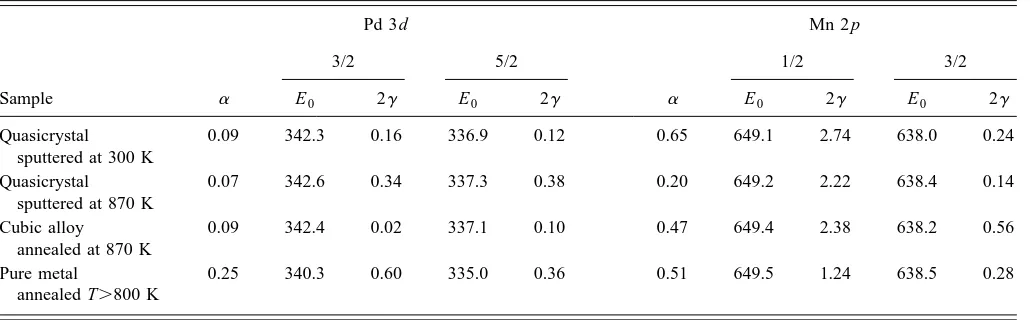
The values of the noninstrumental parameters which cor-respond to the best fits are given in Table II. To a zero-order approximation, the value of the fitting parameter a deter-mines the shape of the peak ~a50 for a purely Lorentzian shape!. Physically, a higher value of a indicates the photo-hole is more effectively screened, corresponding to a higher local density of states~DOS!at EF. The value ofa for the Pd peaks in the annealed quasicrystal, relative to pure Pd is very small ~0.07 vs 0.25!. This is consistent with the pseudogap at EF, and the lack of Pd character there.20–22,26,27
A similar reason may account for the low value ofa in the cubic alloy~0.09!. Although photoelectron data which could reveal the DOS at EF is not available for the cubic alloy, a low DOS at EF would be consistent with its high resistivity. Note that the value of a for the Pd peaks of the alloys is quite robust. Table II shows that it does not vary significantly in the alloy samples, regardless of temperature of prepara-tion, and regardless of whether the alloy is cubic or icosahe-dral.
The trend in the value of a for the Mn peaks is quite different, with the annealed quasicrystal exhibiting a value which is clearly lower than that of any of the other three samples. This accounts for the reduction in intensity of the high-energy tail noted previously, and thus accounts, at least in part, for the distinctive peak shape. However, if this were the only important factor, one would expect the 2 p1/2 and 2 p3/2peaks to show comparable relative reductions in width, since the value ofais set equal for both in any given sample. This expectation is not borne out by the full width at half maximum ~FWHM! values in Table I, suggesting that an additional factor is at play in determining the peak shape.
Taken together, the trends in afor the Pd and Mn peaks suggest that the density of states near EF varies less for Pd
than for Mn, within the range of alloy samples and prepara-tion routes studied here. In other words, the density of Mn states near EF ~the 3d states!appears more sensitive to the structural and/or chemical environment than does the density of Pd states. This is consistent with the fact that Mn 3d states form 3d bands around EF in metallic Mn, and remain near EF ~although hybridized with Al states! in the quasicrystal.21,22,26,27On the other hand, the Pd states lie sev-eral eV below EF in the quasicrystal; as noted above, the
invariance of a in going from the quasicrystalline to the crystalline alloy suggests that the Pd states lie well below EF in the crystalline alloy as well.
The other major fitting parameter is g, which, to zero order, determines the peak half-width. A smaller value ofg corresponds to a narrower peak and a longer lifetime of the photohole, indicating that the photohole is less effectively quenched. For this parameter, the most interesting trend re-vealed by Table II is the distinctively small value ofg, 0.07, for the 2 p3/2Mn peak in the annealed quasicrystal. This re-veals that the second factor responsible for the sharpness of the 2 p3/2peak is a long photohole lifetime. The value ofgin
FIG. 2. Doniach-Sunjic fits to the experimental spectra for Pd and Mn.~a!Quasicrystal Pd.~b!Pure Pd. ~c! Cubic alloy Pd.~d! Quasicrystal Mn. ~e!Pure Mn.~f!Cubic alloy Mn. In each panel, the solid line represents the experimental spectrum; bottom dashed line shows the best fit; and the top dashed line shows the residual
[image:6.612.52.567.599.759.2]~the experimental spectrum minus the fitted spectrum!, which re-flects the quality of the fit. Relative vertical scales are indicated.
TABLE II. Fitting parameters for the Pd and Mn peaks, corresponding to the data of Fig. 2.
Sample
Pd 3d Mn 2 p
a
3/2 5/2
a
1/2 3/2
E0 2g E0 2g E0 2g E0 2g
Quasicrystal sputtered at 300 K
0.09 342.3 0.16 336.9 0.12 0.65 649.1 2.74 638.0 0.24
Quasicrystal sputtered at 870 K
0.07 342.6 0.34 337.3 0.38 0.20 649.2 2.22 638.4 0.14
Cubic alloy
annealed at 870 K
0.09 342.4 0.02 337.1 0.10 0.47 649.4 2.38 638.2 0.56
Pure metal
annealed T.800 K
0.25 340.3 0.60 335.0 0.36 0.51 649.5 1.24 638.5 0.28
Table II for elemental Mn~fourth row!agrees well with that predicted for atomic Mn.48 It is somewhat surprising, there-fore, that the line in the quasicrystal is even sharper than that
~expected!for the free atom.
This may be rationalized as follows. The lifetime of a photohole is dominated by Auger processes. According to McGuire’s calculations,49 roughly half of the total transition probability for filling the 2 p3/2hole in Mn involves 3d elec-trons, i.e., L2/3, C, M4,5and L2/3, M4,5, M4,5processes. This can be seen in the relative strength of Auger lines in the spectrum reported by Va¨yrynen.50Lying in the valence band, it is reasonable that the population, and/or the residual dis-tribution, of Mn 3d electrons varies from the elemental metal to the cubic alloy to the quasicrystalline alloy, hence affect-ing the lifetime of the 2 p3/2hole. The 3d population must be lower, and/or the residual distribution at these states must be larger, in the annealed quasicrystal than in the free atom or in solid elemental Mn, in order for the photohole lifetime to be longer.
In short, for the Mn 2 p3/2line, both of the fitting param-eters aandg appear to reflect characteristics of the Mn 3d states in the annealed quasicrystal. The low value of a is associated with the change in peak shape ~specifically, the reduction in relative intensity of the high-energy tail!, and the low value of g reflects a reduction in the intrinsic line-width. It is their combined influence which makes the experi-mental 2 p3/2line distinctively sharp in the quasicrystal, rela-tive to the other samples studied here.
IV. CONCLUSIONS
Photoelectron spectra of a fivefold quasicrystalline alloy, Al70Pd21Mn9, reveal two noteworthy features. The first is
that the Pd 3d lines fall at binding energies which are 2.2 eV higher than in pure Pd. A similar effect is known to occur for Pd in other alloys, where it is attributed to a combination of initial- and final-state effects.34The second noteworthy fea-ture is that the Mn 2 p3/2line is very sharp in the quasicrystal. Fitting the experimental photoelectron peaks with a Doniach-Sunjic line shape suggests that both the position and population/residual distribution of the Mn states near EF~the
3d states!is very sensitive to the structural and/or chemical environment of Mn in the alloys. However, the results of the fitting should be regarded with some caution, due to the lack of experimental resolution between bulk and surface states, and to the simplistic form assumed for the density of states near EF. The latter concern is particularly relevant to the Pd fits.
In a very practical sense, the interesting result is that the sharpness of the Mn 2 p3/2line may be a useful fingerprint of the quasicrystalline phase within the AlPdMn system. This appears to be true within the range of samples and prepara-tion methods studied here; further comparisons are neces-sary, however, to see how far this conclusion may be ex-tended.
ACKNOWLEDGMENTS
We are indebted to A. I. Goldman and S. W. Kycia of the Ames Laboratory for cutting, polishing, and loaning us the quasicrystal disk. We are also grateful for help with some of the experiments from C.-M. Zhang, and for determination of ferromagnetic properties of the cubic alloy by M. J. Kramer. This work was supported by the Ames Laboratory, which is operated for the U.S. Department of Energy by Iowa State University under Contract No. W-7405-Eng-82.
1D. R. Nelson, Sci. Am. 254, 43~1986!. 2P. J. Steinhardt, Science 247, 1020~1990!.
3A. I. Goldman and M. Widom, Annu. Rev. Phys. Chem. 42, 685
~1991!.
4P. W. Stephens and A. I. Goldman, Sci. Am. 264, 24~1991!. 5C. Janot, Quasicrystals: A Primer, Monographs on the Physics
and Chemistry of Materials Vol. 48, edited by C. J. Humphreys, P. B. Hirsch, N. F. Mott, and R. J. Brook~Clarendon, Oxford, 1992!.
6A. I. Goldman and K. F. Kelton, Rev. Mod. Phys. 65, 213~1993!. 7Quasicrystals and Imperfectly Ordered Crystals, edited by K. H.
Kuo and S. Takeuchi ~Trans Tech, Aedermannsdorf, Switzer-land, 1994!, Vols. 150 and 151.
8Adv. Mater. Proc. 1991, 8~1991!.
9N. Rivier, J. Non-Cryst. Solids 153-154, 458~1993!.
10J.-M. Dubois, S. S. Kang, and Y. Massiani, J. Non-Cryst. Solids
153-154, 443~1993!.
11J. M. Dubois, Phys. Scr. T49A, 17~1993!.
12J.-M. Dubois, S. S. Kang, and A. Perrot, Mater. Sci. Eng. A
179/180, 122~1994!.
13J. M. Dubois, A. Proner, B. Bucaille, P. Cathonnet, C. Dong, V.
Richard, A. Pianelli, Y. Massiani, S. Ait-Yaazza, and E. Belin-Ferre, Ann. Chim. Mater.~Paris!19, 3~1994!.
14S. S. Kang, J. M. Dubois, and J. von Stebut, J. Mater. Res. 8,
2471~1993!.
15S. Takeuchi, H. Akiyama, N. Naito, T. Shibuya, T. Hashimoto,
and K. Edagawa, J. Non-Cryst. Solids 153-154, 353~1993!. 16C. Berger, E. Belin, and D. Mayou, Ann. Chim. Mater.~Paris!18,
485~1993!.
17A. P. Smith and N. W. Ashcroft, Phys. Rev. Lett. 59, 1365
~1987!.
18T. Fujiwara and T. Yokokawa, Phys. Rev. Lett. 66, 333~1991!. 19J. Hafner and M. Krajci, Phys. Rev. Lett. 68, 2321~1992!. 20X. Wu, S. W. Kycia, C. G. Olson, P. J. Benning, A. I. Goldman,
and D. W. Lynch, Phys. Rev. Lett. 75, 4540~1995!.
21E. Belin and Z. Dankha´zi, J. Non-Cryst. Solids 153-154, 298
~1993!. 22
E. Belin, Z. Dankha´zi, A. Sadoc, and J. M. Dubois, J. Phys. Condens. Matter 6, 8771~1994!.
23K. Kimura and S. Takeuchi, in Quasicrystals, The State of the
Art, edited by P. L. Steinhardt and D. Divincenzo~World Sci-entific, Singapore, 1991!.
24Y. Yokoyama, T. Miura, A.-P. Tsai, A. Inoue, and T. Masumoto,
Mater. Trans. 33, 97~1992!.
25C. J. Jenks, B. Cook, S.-L. Chang, and J. Ostensen~unpublished!. 26G. W. Zhang, Z. M. Stadnik, A. P. Tsai, and A. Inoue, Phys. Rev.
B 50, 6696~1994!.
27M. Krajcı´, M. Windisch, J. Hafner, G. Kresse, and M.
Mihal-kovic, Phys. Rev. B 51, 17 355~1995!.
28S.-L. Chang, W. B. Chin, C.-M. Zhang, C. J. Jenks, and P. A.
Thiel, Surf. Sci. 337, 135~1995!.
29S.-L. Chang, J. W. Anderegg, and P. A. Thiel, J. Non-Cryst.
Solids 195, 95~1996!.
30C. J. Jenks, D. Delaney, T. Bloomer, S.-L. Chang, T. Lograsso,
and P. A. Thiel, Appl. Surf. Sci.~to be published! 31M. J. Kramer~unpublished!.
32G. Comelli, M. Sastry, G. Paolucci, K. C. Prince, and L. Olivi,
Phys. Rev. B 43, 14 385~1991!.
33R. Nyholm, M. Qvarford, J. N. Andersen, S. L. Sorensen, and C.
Wigren, J. Phys. Condens. Matter 4, 277~1992!.
34P. Steiner, S. Hu¨fner, N. Ma˚rtensson, and B. Johansson, Solid
State Commun. 37, 73~1981!.
35U. Hillebrecht, J. C. Fuggle, P. A. Bennett, Z. Zolnierek, and C.
Freiburg, Phys. Rev. B 27, 2179~1983!.
36K. Siegbahn, C. Nordlin, A. Fahlman, R. Nordberg, K. Hamerin,
J. Hedman, G. Johansson, T. Bergmark, S.-E. Karlsson, I. Lindgren, and B. Lindberg, Electron Spectroscopy for Chemical Analysis–Atomic, Molecular, and Solid State Studies by Means of Electron Spectroscopy ~Almqvist and Wiksells, Stockholm, 1967!.
37K. Siegbahn, C. Nordlin, A. Fahlman, R. Nordberg, K. Hamerin,
J. Hedman, G. Johansson, T. Bergmark, S.-E. Karlsson, I. Lindgren, and B. Lindberg, Nova Acta Regiae Soc. Ups. Ser. IV
20, 1~1967!.
38D. A. Shirley, in Photoemission in Solids I, edited by M. Cardona
and L. Ley~Springer-Verlag, Berlin, 1978!, p. 165.
39M. Alde´n, H. L. Skriver, and B. Johansson, Phys. Rev. B 50,
12 118~1994!.
40N. Ma˚rtensson and B. Johansson, Solid State Commun. 32, 791
~1980!.
41B. Johansson and N. Ma˚rtensson, Phys. Rev. B 21, 4427
~1980!.
42J. N. Andersen, D. Hennig, E. Lundgren, M. Methfessel, R.
Ny-holm, and M. Scheffler, Phys. Rev. B 50, 17 525~1994!. 43
S. Doniach and M. Sunjic, J. Phys. C 3, 285~1970!.
44G. K. Wertheim and P. H. Citrin, in Photoemission in Solids I,
edited by M. Cardona and L. Ley ~Springer-Verlag, Berlin, 1978!, p. 197.
45G. K. Wertheim and L. R. Walker, J. Phys. B 6, 2297~1976!. 46G. K. Wertheim and S. B. Dicenzo, J. Electron Spectrosc. Relat.
Phenom. 37, 57~1985!.
47J. J. Joyce, M. del Gindice, and J. H. Weaver, J. Electron.
Spec-trosc. Relat. Phenom. 49, 31~1989!.
48O. Keski-Rahkkonen and M. O. Krause, At. Data Nucl. Data
Tables 14, 139~1974!.
49E. J. McGuire, Phys. Rev. A 3, 1801~1971!.
50J. Va¨yrynen, J. Electron. Spectrosc. Relat. Phenom. 22, 27
~1981!.