Q1) Auxiliary memory Ans:
Q2) Cache memory Ans:
Cache memory –
• Small amount of fast memory
• Sits between normal main memory and CPU • May be located on CPU chip or module
Q3) Multiprogramming Ans:
Q5) Memory hierarchy Ans:
As one goes down the hierarchy, the following occur: a. Decreasing cost per bit
b. Increasing capacity c. Increasing access time
d. Decreasing frequency of access of the memory by the processor.
Q6) Locality of reference Ans:
In practice, processors tend to access memory in a very patterned way. For example, in the absence of branches, the PC (Program Counter) is incremented by one after each instruction fetch. Thus, if memory location X is accessed at time t, there is a high probability that memory location X + 1 will also be accessed in the near future. This clustering of memory references into groups is an example of locality of reference.
There are three basic forms of locality:
• Temporal locality — Recently accessed items tend to be accessed again in the near future.
• Spatial locality — Accesses tend to be clustered in the address space (for example, as in arrays or loops).
• Sequential locality—Instructions tend to be accessed sequentially.
Q8) Mapping Ans:
Q9) Direct mapping Ans:
In Direct mapping each main memory block is assigned to a specific line in the cache.
If number of cache line = 4 and number of blocks in main memory = 64 then,
· Direct mapping cache treats a main memory address as 3 distinct fields » Tag identifier
» Line number identifier » Word identifier (offset)
· Word identifier specifies the specific word (or addressable unit) in a cache line that is to be read
· Line identifier specifies the physical line in cache that will hold the referenced address
· The tag is stored in the cache along with the data words of the line
» For every memory reference that the CPU makes, the specific line that would hold the reference (if it is has already been copied into the cache) is determined
Direct mapping summery
• Address length = (s + w) bits
• Number of addressable units = 2s+w words or bytes • Block size = line size = 2w words or bytes
• Number of blocks in main memory = 2s+ w/2w = 2s • Number of lines in cache = m = 2r
• Size of tag = (s – r) bits
Advantages of direct mapping » Easy to implement
» Relatively inexpensive to implement
» Easy to determine where a main memory reference can be found in cache
Disadvantage
» Each main memory block is mapped to a specific cache line
» Through locality of reference, it is possible to repeatedly reference to blocks that map to the same line number
» These blocks will be constantly swapped in and out of cache, causing the hit ratio to be low (a phenomenon known as thrashing)
Q10) Associative mapping Ans:
Associative mapping permits each memory block to be loaded into any line of the cache. In this case, the cache control logic interprets a memory address simply as a tag and a word field. The tag field uniquely identifies a block of main memory. To determine whether the block is in the cache, the cache control logic must simultaneously examine every line’s tag for a match. To summarize,
• A main memory block can load into any line of cache • Memory address is interpreted as tag and word • Tag uniquely identifies block of memory
Associative mapping summery • Address length = (s + w) bits
• Number of addressable units = 2s+w words or bytes • Block size = line size = 2w words or bytes
• Number of blocks in main memory = 2s+ w/2w = 2s • Number of lines in cache = undetermined • Size of tag = s bits
Advantages of Associative mapping • Flexible
• Fast
Disadvantages
• Complex circuitry required to examine the tags of all cache lines in parallel
Q11) Set Associative mapping Ans:
Set Associative mapping is a compromise between direct and associative mapping. In this case, the cache is divided into v sets; each set consists of k lines. If a set can hold k lines then, it is referred to as k way set associative mapping. In this case, a main memory block Bj can be mapped into any of the lines of set i. Here the cache control logic interprets the memory address simply as three fields: tag, set and word. The set bits specify one of v sets. With k-way Set Associative mapping, the tag in a memory address is compared to the k tags within a single set. To summarize,
• Cache is divided into a number of sets • Each set contains a number of lines
Set Associative mapping summery • Address length = (s + w) bits
• Number of addressable units = 2s+w words or bytes • Block size = line size = 2w words or bytes
• Number of blocks in main memory = 2s • Number of lines in set = k
• Number of sets = v = 2d
• Number of lines in cache = kv = k * 2d • Size of tag = (s – d) bits
Q12) Replacement algorithm Ans:
(1) Direct mapping a. No choice
b. Each block only maps to one line c. Replace that line
(2) Associative & Set Associative mapping
When an associative cache or a set associative cache set is full, which line should be replaced by the new line that is to be read from memory is a big question. For this different replacement algorithms are there.
accesses for every cache block, which requires significant space and slows down the operation of the cache.
First in, first out (FIFO) is another popular approach. With this algorithm, the block that has been in cache the longest (regardless of how recently it has been used) would be selected as the victim to be removed from cache memory.
Another approach is to select a victim at random. The problem with LRU and FIFO is that there are degenerate referencing situations in which they can be made to thrash (constantly throw out a block, then bring it back, then throw it out, then bring it back, repeatedly). Some people argue that random replacement, although it sometimes throws out data that will be needed soon, never thrashes. Unfortunately, it is difficult to have truly random replacement, and it can decrease average performance.
The algorithm selected often depends on how the system will be used. No single (practical) algorithm is best for all scenarios. For that reason, designers use algorithms that perform well under a wide variety of circumstances.
Q13) Associative memory or Content Addressable Memory (CAM) Ans:
Q14) Address space, memory space Ans:
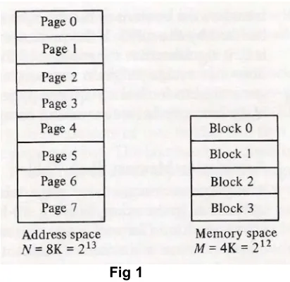
Q15) Page, blocks and page frames Ans:
Q16) Address mapping using pages Ans:
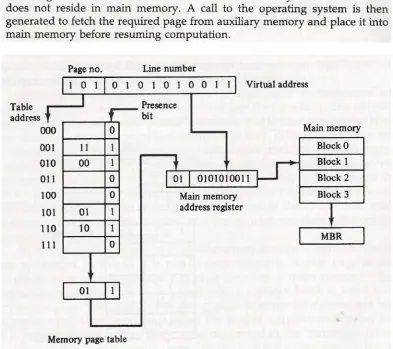
[image:9.612.202.408.323.523.2]Q17) Associative memory page table Ans:
Q19) Memory management unit Ans:
Q20) Segment Ans:
Q21) Logical address Ans:
Q23) Translation lookaside buffer Ans:
Q24) RAM Ans:
Even though a large number of memory technologies exist, there are only two basic types of memory: RAM (random access memory) and ROM (read-only memory). RAM is somewhat of a misnomer; a more appropriate name is read write memory. RAM is the memory to which computer specifications refer; if you buy a computer with 128 megabytes of memory, it has 128MB of RAM.
RAM is also called the “main memory”. Often called primary memory, RAM is used to store programs and data that the computer needs when executing programs; but RAM is volatile, and loses this information once the power is turned off. There are two general types of chips used to build the bulk of RAM memory in today’s computers: SRAM and DRAM (static and dynamic random access memory).
Dynamic RAM is constructed of tiny capacitors that leak electricity. DRAM requires a recharge every few milliseconds to maintain its data. Static RAM technology, in contrast, holds its contents as long as power is available. SRAM consists of circuits similar to the D flip-flops. SRAM is faster and much more expensive than DRAM; however, designers use DRAM because it is much denser (can store many bits per chip), uses less power, and generates less heat than SRAM. For these reasons, both technologies are often used in combination: DRAM for main memory and SRAM for cache. The basic operation of all DRAM memories is the same, but there are many flavors, including Multibank DRAM (MDRAM), Fast-Page Mode (FPM) DRAM, Extended Data Out (EDO) DRAM, Burst EDO DRAM (BEDO DRAM), Synchronous Dynamic Random Access Memory (SDRAM), Synchronous-Link (SL) DRAM, Double Data Rate (DDR) SDRAM, and Direct Rambus (DR) DRAM. The different types of SRAM include asynchronous SRAM, synchronous SRAM, and pipeline burst SRAM.
Q25) ROM Ans:
Q26) Magnetic disk technology Ans:
Disk drives are called random (sometimes direct) access devices because each unit of storage, the sector, has a unique address that can be accessed independently of the sectors around it. As shown in Fig, sectors are divisions of concentric circles called tracks. On most systems, every track contains exactly the same number of sectors. Each sector contains the same number of bytes. Hence, the data is written more “densely” at the center of the disk than at the outer edge. Some manufacturers pack more bytes onto their disks by making all sectors approximately the same size, placing more sectors on the outer tracks than on the inner tracks. This is called zoned-bit recording. Zoned-bit recording is rarely used because it requires more sophisticated drive control electronics than traditional systems.
Disk tracks are consecutively numbered starting with track 0 at the outermost edge of the disk. Sectors, however, may not be in consecutive order around the perimeter of a track. They sometimes “skip around” to allow time for the drive circuitry to process the contents of a sector prior to reading the next sector. This is called interleaving. Interleaving varies according to the speed of rotation of the disk as well as the speed of the disk circuitry and its buffers. Most of today’s fixed disk drives read disks a track at a time, not a sector at a time, so interleaving is now becoming less common.
Q27) Rigid or hard disk drives Ans:
actuator is energized, the entire comb of read-write heads moves toward or away from the center of the disk.
In a stack of disk platters, all of the tracks directly above and below each other form a cylinder. A comb of read-write heads accesses one cylinder at a time. Cylinders describe circular areas on each disk. Typically, there is one read-write head per usable surface of the disk. (Older disks—particularly removable disks—did not use the top surface of the top platter or the bottom surface of the bottom platter.) Fixed disk heads never touch the surface of the disk. Instead, they float above the disk surface on a cushion of air only a few microns thick. When the disk is powered down, the heads retreat to a safe place. This is called parking the heads. If a read-write head were to touch the surface of the disk, the disk would become unusable. This condition is known as a head crash.
Q28) Seek time Ans:
Seek time is the time it takes for a disk arm to position itself over the required track.
Q29) Rotational delay
Rotational delay is the time that it takes for the required sector to position itself under a read/write head.
Q30) Access time
The sum of the rotational delay and seek time is known as the access time.
Q31) Transfer time
If we add to the access time the time that it takes to actually read the data from the disk, we get a quantity known as transfer time, which, of course, varies depending on how much data is read.
Q32) Latency
Q33) Cache write policies Ans:
In addition to determining which victim to select for replacement, designers must also decide what to do with so-called dirty blocks of cache, or blocks that have been modified. When the processor writes to main memory, the data may be written to the cache instead under the assumption that the processor will probably read it again soon. If a cache block is modified, the cache write policy determines when the actual main memory block is updated to match the cache block. There are two basic write policies:
• Write-through—A write-through policy updates both the cache and the main memory simultaneously on every write. This is slower than write-back, but ensures that the cache is consistent with the main system memory. The obvious disadvantage here is that every write now requires a main memory access. Using a write-through policy means every write to the cache necessitates a main memory write, thus slowing the system (if all accesses are write, this essentially slows the system down to main memory speed). However, in real applications, the majority of accesses are reads so this slow-down is negligible.