AUT J. Elec. Eng., 51(1) (2019) 63-70 DOI: 10.22060/eej.2019.14603.5234
A High Efficient, Compact 4th Order CLCL Converter Features to Use
Constant-Current Power Supply
K. Davoodi1, J. Shokr elahi Moghani2, S. Salehi Dobakhshari2
1 Department of Electrical Engineering, Shahid Beheshti University,Tehran, Iran and Mazandaran Regional Electric Company, Sari, Iran. 2 Department of Electrical Engineering, Amirkabir University of Technology (AUT), Tehran, Iran
ABSTRACT: This paper presents a 4th order CLCL resonant converter which can be used as a constant current power supply (CCPS) with immittance property. This structure is one of the resonance converter topologies that has not been studied. This converter is designed with immittance characteristic with two inductors and two capacitors in the resonant network. A detailed analysis and design process of a 200w converter as a constant current supply have been provided and simulation results are verified with results of a constructed converter. In analyzing this converter, the AC analysis method is used. This converter with its unique structure, a combination of series and parallel resonant converter has the advantages of both. As a constant current supply, CLCL resonant converter has the advantages of rigidity against short circuit, no need to control against load changes, easy operation in parallel mode, low circulating currents and high efficiency about 93%, due to its soft-switching operation. For this converter, leakage and magnetizing inductance of a transformer can be used as a part of the resonance network and it decreases the converter size. As a result, the cost of constructing the converter is reduced. Also, series capacitor eliminates the DC component and prevents the transformer saturation in unbalanced conditions. With fixed-frequency performance, filter design will also be easier. Other structures have only some of these benefits, but this structure has all these. Considering these advantages, the proposed topology can be used in a variety of applications such as magnetic power supplies, capacitor charging power supplies and driver for laser diodes.
Review History:
Received: 16 June 2018 Revised: 4 December 2018 Accepted: 6 February 2019 Available Online: 6 February 2019
Keywords:
Constant current DC-DC immittance resonance converter high efficiency
1- Introduction
Resonant converters (RC) have special features such as zero-voltage switching (ZVS)[1], zero current switching (ZCS)[2], high-frequency performance [3], high efficiency [4], small size and low electromagnetic interference (EMI)[5]. These converters are used as DC power supplies for industrial, commercial, and domestic applications, and AC power supplies for induction heating [6], power factor correction [7] and ballast lamp discharging [8].
Series [9] and parallel [10] resonant converters (SRC and PRC) are the basis of the performance of the topologies of the other RCs which have two reactive elements. Each of these converters as the basis for resonant converters has advantages and disadvantages, and to remove limitations in SRC and PRC [11], resonant converters with three and four reactive elements are applied [12]. Despite the simplicity in design of third-order resonant converters, in terms of design flexibility and attraction of parasitic circuit elements, these converters have more restrictions than 4th order converters in the absorption of the circuit’s parasitic elements and design flexibility [13]; therefore, 4th order converters are more suitable to investigate.
By utilizing these basic structures, in this paper, we have achieved a 4th order topology that has a significant improvement in no-load regulation characteristic compared to the two previously mentioned topologies. This converter with its unique structure, a combination of series and parallel resonant converter, has the advantages of both. As a constant current supply, CLCL resonant converter has the advantages of rigidity against short circuit, no need to control against
load changes, easy operation in parallel mode, low circulating currents and high efficiency. When this 4th order converter, called the resonant CLCL converter, operates at a switching frequency equal to the resonance frequency, it will provide a load-dependent output voltage. Thus, the output voltage can be set against wide changes in load. Magnetic components of this converter could be integrated with the transformer and hence it can be a great candidate as a power supply with regulated output voltage. Circuit diagram of this topology is shown in Fig. 1. CLCL resonant network consists of inductors L1 and L2, and capacitors C1 and C2 which is incited by a half-bridge square wave inverter. The model shows that the resonant CLCL converter provides an output voltage which depends on the load and no-load regulation. When the circuit works at the resonant frequency, the resonant CLCL converter acts as a current source. Under these conditions, the output current is kept constant regardless of load changes. Moreover, performing at resonant mode, the output current of the inverter which is the inductor (L2) current, is in-phase with the voltage, that reduces changes in part-load conditions. The maximum efficiency of this converter in the part-load condition is less than full load condition, due to conduction losses. The resonant CLCL converters can be used to achieve a high power factor in rectifiers.
The feature that changes this resonant converter from a high-frequency constant voltage-source converter to a high frequency constant current-source converter is the utilization of immittance characteristic within this converter [14]. A constant current source is used in many commercial, industrial, and research applications such as electromagnetic [15], capacitor charging [16], battery charging [17], arc welding, etc. [18]. Resonant CLCL converters with the
advantages of a current-source can be a potential candidate for these applications.
The main use of the converter as a CCPS is for driving high power laser diode which these laser diodes are driven with the current basically. Laser diodes are one of the various types of lasers that are used widely in the lighting industry, medical industry, printing industry as well as higher-power applications such as welding, cutting, burning and sintering, brazing, lithography, marking plastic, metal, and silicon. The main characteristics of these laser diodes are noted as follows: Low resistance and High input current.
Although the laser diode behaves like a normal diode electrically, this laser diode turns on when a knee voltage is greater than 1 V. The equivalent circuit of a laser diode is shown in Fig. 2. In this figure, values of L, C, and R are very small and Rd is very large; but the inductor and capacitor in the equivalent circuit can be neglected in low frequencies in about hundreds of kHz. Therefore, the steady-state equivalent circuit of this type of diode _ similar to the conventional diode dynamic model_ is modeled as a resistance [19].
The rest of this paper is organized as follows. In section 2, the analysis of this converter is described. Designing of the converter with the required features for the high power laser diode is presented in section 3. The simulation and construction of the presented converter are given in section 4, respectively. At last, the conclusions of this paper are provided in section 5.
2- Analysis of the converter
Among analysis methods, the AC analysis method is chosen. In the AC analysis [20], the rectifier and filter output have been replaced by an equivalent resistance and the square-wave input voltage-source is replaced with an equivalent sine-wave one. It is assumed that the transmission of power from input to the output is done only by the main component. Also, higher-order harmonics are neglected because of the low-pass property of the resonant network. The simplified equivalent circuit for the analysis is shown in Fig. 3.
The following assumptions have been made, too:
• Equivalent ac resistance (Re) for the rectifier with a capacitor filter and the RMS value of the main component of the square-wave input voltage are explained in the following terms [21]:
, 2 2
2 2 , R 8 L.
in rms d e R
V V
n
π π
= = (1) • Resonance frequency (ω0) and normalized switching
frequency (ωn) are defined by :
1 1
1 , ,
o n o L C ω ω ω ω
= = (2)
where ωis the switching frequency.
• Also, the characteristic impedance (Zn) and F are defined as follows :
2 2 1 1 1 , o n n e e
n L n Z L
F Z
R R C
ω
= = = (3)
The ratio of the capacitors and the ratio of inductors are defined as follows:
2 2
1 1
, .
L C
L C
γ = ψ= (4)
The voltage gain (Vno ) and the current gain (Ino ) of the converter which are in fact normalized output Voltage and current are expressed as follows:
, o .
o no no d d n V nI n
I V V
V Z
= = (5)
Also, voltage gain and current gain of the resonant CLCL converter is shown in detail by expressions, below:
( )
(
)
(
)
3
4 1 n2 1 1 2 ,
no
n n n n
j V
F j
ψω
γψω ψ γψ ω ψω ω
− =
− + + + + − (6)
( )
(
)
(
)
3
2 4 2 2
8 .
1 n 1 1
no
n n n n
j F I
F j
ψω
π γψω ψ γψ ω ψω ω
− =
− + + + + − (7)
Eq. (7) shows that if the converter operates at ωn =1, the
SA 2Vd SB DB DA CA CB
C1 C2
L1
L2 1:n
Tr Dr1 Dr2 Dr3 Dr4 Cf
RL VO
IO
Fig. 1. Circuit diagram of the CLCL topology
L
R
dC
R
Fig. 2. Circuit diagram of a laser diode
L
1L
2V
inC
1C
2R
acoutput current will be independent of load and under these conditions:
2
1 8 .
n
no
I ω= =π (8) Then, the equation for RMS value of normalized current of capacitor C1(IC1N), based on the reference current (Vd / Zn) has been expressed in (9). It is also possible to achieve stress relationships of voltage and current on each element. The relationships for the value of normalized current inductor L1
(IL1N), inductor L2 (IL2N) and capacitors C2 (IC2N) and also RMS value of the normalized voltage of these elements (VL1N, VL2N, VC1N, and VC2N) based on the reference voltage and current (Vd and Vd / Zn) achieved. Current of capacitor C1 (IC1N) is summarized as follows :
( )
(
)
( )
( ) ( )
1 1
2 2
,
4 2 2
1 1
2 2 .
1 1 1
n n n
C rms C N
d n n n n
n
j F
I
I V
F j
Z
ψω γ ω ψ ψω
π γψω ψ γψ ω ψω ω
− − + −
= =
− + + + + − (9) By operating at ωn =1, the current of the capacitor C1 is simplified as follows :
( )
(
)
( )
(
)
1 1
1 1
2 2 .
1 1
n
C N
j F
I
F
ω
ψ γ ψ ψ
π γψ ψ γψ
=
− + + −
=
− + + + (10)
Therefore, the phase angle between Vin and IL1 could be obtained by :
( )
(
)
1 1
1 1 tan
n
Q
ω
γ ψ ψ
ϕ
ψ −
=
+ −
=
−
(11)
If the designed converter operates with γ 1ψ ψ −
= at ω
n=1, for all
F values, φ will be equal to zero. Therefore, the converter provides a constant output current which is in-phase with the
source voltage and current in all loading conditions. These conditions called immittance conditions changes a voltage source to a current source.
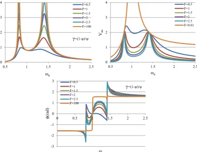
The variation of Ino for different values of F and γ 1ψ ψ − = is shown in Fig. 4 (a). For F = 100 which i s related to a condition close to the short-circuit load, t he characteristic shows the current-source behavior of the co n verter. Fig. 4(b) shows the variation of Vno for different values of F and
γ 1ψ ψ −
= . For F = 0.01, which is related to a condition close to the open-circuit load, it shows the voltage-source behavior of the converter. As illustrated in Fig. 4(b), the converter has the voltage source property in two operating frequencies with
voltage gain 2. Fig. 4.(c) indicates the φ changes as a function of ωn for different values of F and γ 1ψ
ψ −
= . It can be seen that for all the values of F, the output current is independent of the
load for ωn=1. In other words, this topology can be used as a
voltage source, in addition to the current source applications.
Meanwhile, for all values of F, φ = 0 at ωn=1. For resonant
converters, the existence of a lag between inverter’s output voltage and current is required to achieve ZVS. Eq. (11) shows that the resonant CLCL converter can operate in a lagging
power factor, if γ 1ψ ψ −
< . Therefore, the required phase delay can be achieved by keeping the γ slightly less than the 1ψ
ψ − .
3- Design of the converter elements
To design converter elements, serious attention is paid to the current ripple; due to this, a laser diode is sensitive to the current ripple and the laser diode will be burnt by changing the current more than the allowed amount. At the next level, the amount and density of the converter power are considered. To design CLCL converter, the values of voltages, currents, Fig. 4. (a) Ino, (b) Vno and (c) ϕ in CLCL according to different values of F and CLCL γ =
and reactive elements for immittance resonance network has
been determined. Conditions ωn=1 and γ 1ψ ψ −
= is required for the converter operation as a current source. By defining (kVA / kW) rate which is an indicator of the physical size of the converter and using voltage and current of each element in immittance conditions [22], the following equation would be obtained:
1 1 2 2 2 2 1 1
1 1,
2
1 1,
. . . .
. n
C N C N C N C N L N L N L N L N
n
KVA KW
V I V I V I V I H F
ψ ω γ ψ
ψ ω γ
ψ −
= =
− = =
=
+ + + (12)
By applying Eq. (12) for the CLCL topology and simplifying, the following equation is obtained:
2
2 1
1,
1 16 1 .
4
n
KVA F
KW ω γ ψ F
ψ
π
ψ π
− = =
= + (13)
Fig. 5 shows Eq. (13) as a function of F. Graphs show that for a certain value of F , the ratio (kVA / kW) is minimal. This value is called optimal F value (Fopt) and corresponds to the optimal value of (kVA / kW) and is shown as (kVA / kW)opt. Equations for Fopt and (kVA / kW)opt are as follows:
1 2
1,
8 ,
n
opt
F ω γ ψ
ψ
ψ π −
= = = (14)
1 1,
4 .
n
opt
KVA
KW ω γ ψ
ψ
ψ − = =
=
(15)
As the characteristics are shown in Fig. 5, the values of Fopt and (kVA / kW )opt differ for each ψ value. As the ψ value
increases, the (kVA / kW )opt ratio decreases; or in other words, the power density rises. Also, this causes a reduction in the inductance and the circuit total size. From the expression,
bigger ψ is sufficient for operation; but on the other hand, increasing ψ reduces γ more and therefore the size of L1 and L2 inductances drastically diminishes and variation in output current increases under load changes, thus, the current-source property of the converter declines. Since the circuit current variations should not exceed 2 percents under load changes, even without using a control loop, ψ=0.25 is chosen to design the circuit elements.
General design input are the DC input voltage, the output current (Io), maximum load resistance (RLmax) and switching frequency (fs). With a full load F, equivalent to Fopt, equations
for n, L1, L2 and C1 according to parameters of the converter terminal are as follows:
,max ,
o L
d
I R n
V ψ
= (16)
2
1 3 2
,max
4 d 1 ,
o L s
V L
I R f
π ψ
= (17)
2 ,max
1 16 2 .
o L
d s
I R C
V f
π ψ
= (18)
0.01 0.01001 0.01002 0.01003 0.01004 0.01005
Time (sec)
0 20 40 60 80 100
Voltage(V) Current(A)
Vsw Isw
(a) (b) Fig. 7. Voltage and current waveform of the switch: (a) simulation, (b) prototype
Fig. 6. A view of the built converter
Table 1. The converter specification
Parameter Quantity
Vd 80 V
Io 10 A
n 4
RL 2 Ω
fs 100 KHz
L1 21.6 uF
C1 120 nF
γ 3
Ψ 0.25
CA,CB 100 uF
4- Simulation and Prototyping of the converter
A simulation is done to verify the ability of the resonant CLCL converter as a current source and then to confirm the results, a model of the converter is built by modeling of the laser diode with resistance. So the results can be compared with each other. To construct a model of the converter, the specifications are shown in Table 1.
However, with aforementioned quantities, the circuit operate in in-phase mode and due to tolerances in the magnetic elements, it would be better to work in the lag mode to realize the ZVS in switches [23]. Therefore, the value of C1 would be slightly larger than the value given above to ensure that the switches will have ZVS operation.
To construct the converter, the leakage inductance of the transformer has been integrated as part of the L2 inductance; in a way that leakage inductance of the transformer is 7 micro Henry and by integrating with L2, the inductance size reaches 58 micro Henry. A view of the realized converter is shown in Fig.6. Results of the converter realization are provided in
0.01 0.01001 0.01002 0.01003 0.01004 0.01005
Time (sec)
-50 -25 0 25 50
Voltage(V) Current(A)
Vnet Inet
(a) (b) Fig.8. Input voltage and current waveforms of the resonantnetwork: (a) simulation, (b) prototype
0.01 0.01001 0.01002 0.01003 0.01004 0.01005
Time (sec)
-150 -100 -50 0 50 100 150
Voltage(V) Current(A)
VC1 IC1
Figures 7 to 10.
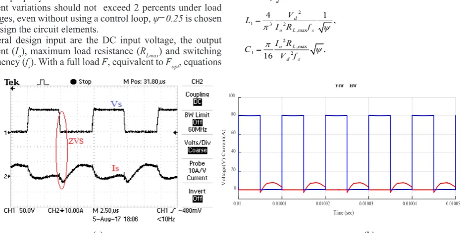
Voltage and current waveform of the switch is shown in Fig.
7. As the figure shows, the switch is turned-on softly and also
in practice switches have soft switching (ZVS). From the
figure it seems that voltage across the switch is 80 V which is
twice the voltage designed; also the peak current is about 8 A. In Fig. 8, the input voltage and current waveforms of the resonant network are shown in which the ZVS is clearly visible. The voltage across the switch is twice the voltage across the network, Therefore the voltage across the network alters between +40V and -40V.
Voltage and current waveforms of the converter’s capacitor C1 are shown in Fig. 9. Also, in this figure, the sinusoidal shape of the voltage and current of the capacitor due to the resonance with L1 can be seen. The 90-degree phase difference between voltage and current is also due to resonance. Fig. 10, shows the changes in output voltage and current when the load decreases from 2 ohms to 1.5 ohms. As the figure reveals, with the load altering from 2 ohms to 1.5 ohms, the current is almost constant and has not changed so much, but the output voltage is reduced. Therefore, it proves that the converter can practically operate as a constant current power supply without a feedback control.
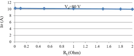
Fig. 11 shows a plot of output current versus load resistance. As Fig. 11 indicates, by reducing the load from the rated
value, 2 Ω to a point close to the short circuit in load, output
current has not changed so much and its total changes are less than 2 percent of the nominal current that is perfect for applications where accurate constant current source exists. Thus, it shows the independence of the output current of
the converter from its load and the fact which the converter operates as a constant-current power supply, regardless of the load. This feature is very convenient for a driver of a laser diode.
Fig. 12 shows a graph of the converter efficiency according to the output power. In the blue graph, the load resistance is kept
at its nominal value of 2 Ω and the input voltage is decreased
from its rated value. According to the plot, for output power near 20 W, the efficiency of the converter is above 80 percents which indicates that this topology in amounts far away from its nominal value, offers a good efficiency. Meanwhile, in the red graph, the input voltage is kept at its nominal value of 80 V and the load resistance is decreased from its rated value to a point close to the short circuit in load. According to the plot, for output power near 40 W, the efficiency of the converter is above 80 percent.
Employing a resonant converter as a constant current power supply is used in several articles with different topologies. [21-23]. The proposed converter in this paper is more efficient than other converters. Also, one of the main advantages of this converter is the inherent dc blocking of the isolation transformer due to the series capacitor in the resonant network. This converter has more output current capability, in other words, the range of the current of converter is 0 to 10 A, which is much larger than many converters. Also, with the
Fig. 11. Diagram output current as a function of load resistance
Fig. 12. Diagram efficiency as a function of power output. Plot (a) : RL=2 Ω and Vd is varied from 10 to 80 V. Plot (b) : Vd =80
V and RL is varied from 2 to 0.1 Ω
0.003 0.006 0.009 0.012 0.015
Time (sec)
0 5 10 15 20 25
Voltage(V) Current(A)
Vout Iout
Iout Vout
optimal design of inductors and capacitors, it is possible to use isolation transformer magnetization inductance in addition to the leakage inductance, which reduces the dimensions of the converter and reduces the cost. Therefore, this converter is an important candidate for use as a power supply.
5- Conclusion
This paper presents a detailed analysis of a resonant CLCL converter as a constant current source for laser diode driver and closed-form expressions of the converter gain and the stresses on the components. The converter shows a voltage gain that depends on the load and current gain that is independent of the load at a given operating frequency, which is suitable for a constant current power supply.
Conditions for the optimal design of the converter, for the minimum size of the resonant network, are revealed. In general, the leakage and magnetizing inductance of the transformer can be useful in resonant CLCL network. It is shown that using a series capacitor prevents the DC component in the isolation transformer. Efficiency at full-load is more than 92 percent, with an output current of 10 A, due to negligible eddy current and soft-switching operation. The advantages of the presented topology,
especially
with features constant current source and high efficiency can lead this converter to a vast variety of applications, especially for the constant current ones, for example, laser diode driver.References
[1] I. Batarseh, Resonant converter topologies with three and four energy storage elements, IEEE Transactions on power electronics, 9(1) (1994) 64-73.
[2] A. Bhat, M. Swamy, Analysis and design of a high frequency parallel resonant converter operating above resonance, in: APEC’88 Third Annual IEEE Applied Power Electronics Conference and Exposition, IEEE, (1988) 182-189.
[3] K. Liu, Y. Gao, Y. Sun, D. Zhang, P. Yan, High-frequency high-voltage DC power supply based on parallel resonant technology and phase shift control, IEEE International Power Modulator and High Voltage Conference (IPMHVC), IEEE, (2012) 469-472.
[4] M. Bartoli, A. Reatti, M. Kazimierczuk, Full-range high-frequency high-efficiency class D/sup 2/resonant power supply, Proceedings of IECON’94-20th Annual Conference of IEEE Industrial Electronics, IEEE, (1994) 159-163.
[5] T. Sato, H. Matsuo, Analysis of a novel current resonant DC–DC converter, IEEE Transactions on Industrial Electronics, 60(11) (2012) 4987-4995. [6] O. Lucia, H. Sarnago, J.M. Burdio, Soft-stop optimal
trajectory control for improved performance of the series-resonant multiinverter for domestic induction heating applications, IEEE Transactions on Industrial Electronics, 62(10) (2015) 6251-6259.
[7] M. Alam, W. Eberle, C. Botting, M. Edington, A bridgeless hybrid-resonant PWM zero voltage switching boost AC-DC power factor corrected converter, IEEE Energy Conversion Congress and Exposition (ECCE), IEEE, (2014) 606-610.
[8] R. Casanueva, C. Branas, F.J. Azcondo, F.J. Diaz,
Teaching resonant converters: Properties and applications for variable loads, IEEE Transactions on Industrial Electronics, 57(10) (2010) 3355-3363. [9] H. Wang, T. Saha, R. Zane, Control of series connected
resonant converter modules in constant current dc distribution power systems, IEEE 17th Workshop on Control and Modeling for Power Electronics (COMPEL), IEEE, (2016). 1-7.
[10] M. Borage, S. Tiwari, S. Kotaiah, A parallel resonant constant current power supply, Journal of the Indian Institute of Science, 83(5,6) (2013) 117.
[11] W. Zhang, F. Wang, D.J. Costinett, L.M. Tolbert, B.J. Blalock, Investigation of gallium nitride devices in high-frequency LLC resonant converters, IEEE Transactions on Power Electronics, 32(1) (2016) 571-583.
[12] R. Mazgut, M. Galad, S. Kascak, P. Spanik, Analysis of multi-resonant LLCLC converter, ELEKTRO, IEEE, (2016) 192-195.
[13] Y. Ang, C. Bingham, M. Foster, D. Stone, Analysis and control of dual-output LCLC resonant converters, and the impact of leakage inductance, 7th International Conference on Power Electronics and Drive Systems, IEEE, (2007) 145-150.
[14] M. Borage, K. Nagesh, M. Bhatia, S. Tiwari, Resonant immittance converter topologies, IEEE Transactions on Industrial Electronics, 58(3) (2010) 971-978. [15] M. Borage, S. Tiwari, S. Kotaiah, LCL-T resonant
converter with clamp diodes: A novel constant-current power supply with inherent constant-voltage limit, IEEE Transactions on Industrial Electronics, 54(2) (2007) 741-746.
[16] A.C. Lippincott, R.M. Nelms, A capacitor-charging power supply using a series-resonant topology, constant on-time/variable frequency control, and zero-current switching, IEEE transactions on industrial electronics, 38(6) (1991) 438-447.
[17] Y.-J. Choi, S.-Y. Choi, R.-Y. Kim, An integrated voltage-current compensator of LLC resonant converter for Li-ion battery charger applications, IEEE 8th International Power Electronics and Motion Control Conference (IPEMC-ECCE Asia), IEEE, (2016) 3783-3790.
[18] M. Borage, S. Tiwari, S. Bhardwaj, S. Kotaiah, A full-bridge DC-DC converter with zero-voltage-switching over the entire conversion range, IEEE Transactions on Power Electronics, 23(4) (2008) 1743-1750. [19] W.-E. Kassa, A.-L. Billabert, S. Faci, C. Algani,
Electrical modeling of semiconductor laser diode for heterodyne RoF system simulation, IEEE Journal of Quantum Electronics, 49(10) (2013) 894-900.
[20] X. Li, A. Rathore, A general study of soft-switching ranges of dual-bridge resonant converters using a modified complex AC analysis approach, 6th IEEE Conference on Industrial Electronics and Applications, IEEE, (2011) 322-327.
electronics, 52(6) (2005) 1547-1554.
[22] M. Borage, S. Tiwari, S. Kotaiah, Constant-current, constant-voltage half-bridge resonant power supply for capacitor charging, IEE Proceedings-Electric Power Applications, 153(3) (2006) 343-347.
[23] M.B. Borage, K. Nagesh, M. Bhatia, S. Tiwari, Characteristics and design of an asymmetrical duty-cycle-controlled LCL-T resonant converter, IEEE Transactions on Power electronics, 24(10) (2009) 2268-2275.
Pleasecitethisarticleusing:
K. Davoodi, J. Shokr elahi Moghani, S. Salehi Dobakhshari, A High Efficient, Compact 4th Order CLCL Converter
Features to Use Constant-Current Power Supply, AUT J. Elec. Eng., 51(1) (2019) 63-70.