ABSTRACT: The power dissolute by the links of a network-on-chip (NoC) starts to play with the power dissipated by the additional basic elements of to the communication sub-system within specifically, the routers &network interfaces (NIs). In this, we present a conventionaldata encoding schemes meant to reducing the dissipated of power by the links in the NoC. The proposed schemes are universal and transparent with respect to the fundamental NoC fabric (i.e., their application doesn’t require any amendment of the routers or in the link architecture). Tests carried out on both synthetic and real traffic circum-stances show the efficiency of the proposed schemes.
Keywords: NoC(Network on Chip), BI(Bus Invert), Encoding, Power dissipation, Hamming distance
Received: 18 January 2016, Revised 17 February 2016, Accepted 24 February 2016
© 2016 DLINE. All Rights Reserved 1. Introduction
The Network-on-Chip (NoC) paradigm has evolved to the replace ad-hoc global wiring interconnection and this system modules communicate bysending packets in one to another over a network. A conventional NoC consists of a packet switched network with a two-dimensional mesh type topology. NoCs typically employ wormhole routing, i.e., each packet is divided small unit. Currently proposed NoCs is employ between two and four VCs, but studies argue that this number should increase in future NoCs in order to the supply higher throughput demands. Power consumption is becoming a crucial factor in the design of high-speed digital systems. This static power consumption is due to leakage and short-circuit currents, dynamic power consumption stems from the switching activity, i.e., bit transitions. Modern device scaling results in the deep sub micron noises, which cause to interconnect errors be the more dominant and harder to predict, and also gives rise to new error sources.Embedded power design approaches include techniques for energy efficient micro architecture. For example, in a power-driven design of router for NoC is presented. The technique we present in this thesis can complement these approaches, and combining both schemes can help to further reduce Power.Popular methods include Bus Invert (BI), gray coding, adaptive coding and transition coding method. BI compares the data to be transmitted with in the current data on link. If the Hamming distance is(the number of bits in which the data patterns dicer) between to new information and to the link state is larger than the half number of bits (wires) on this link, then
Power Reduction Technique for Data Encoding in Network-on-Chip (NoC)
Venkatesh Rajamanickam1, M.Jasmin2
1, 2Department of Electronics and Communication Engineering 1, 2Bharath University,Selaiyur
Chennai, India
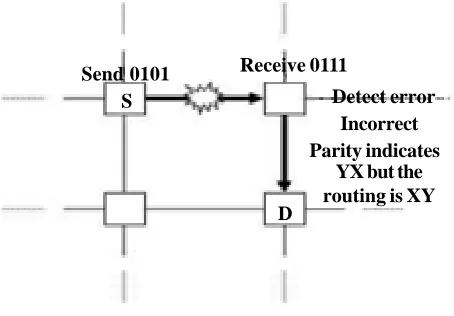
the data pattern is inverted before transmission. The reduction of NoC power consumption is achieved and using the four mentioned data encoding schemes. Experiments in 0:35nm technology showed that BI achieves the best results. The main idea behind our approach is to take advantage of the multiple routing paths between nodes. Path diversity was exploited, the past in order to theachieve load-balancing, by the routing some traffic XY and remaining traffic YX. We illustrate this in Figure 1.1, where a packet is transferred from the source node S and destination node, D, on a regular mesh NoC. The data parity determines the routing path: 1 for YX routing and 0 for XY. In Fig. 1.1 to refer the data is 0101, so the parity bit data is 0, which indicates to the XY routing. While transferring the packet data from S to the adjacent near horizontal node (according to XY routing), one error occurs, changing to the data 0111. At the node receiving, tothe calculate in parity bit data is then 1, which indicates to the YX routing. Since the edge packet is arrives on the expected path, an error is to deduced.A single parity data bit can be saved whenever there are two and more than available paths between the source to destination nodes. However, may not always be this case if we wish to the employ shortest-path routing: if the source node and destination nodes are share one coordinate (either X or Y) there is one shortest routing path only. In some cases, PaR adds an extra parity bit to the packet.
Figure 1. Example: bit flip detection
In the general case, where the reliability demand is r to redundant parity bits data, we expand the method for error protection using to the multiple routing paths between S to D. Some of the paths share edges, and therefore we save to redundant bit transmissions on some of the edges within routing paths, but not all to. We have verifyto the correctness of PaR using exhaustive of state exploration for all source and the destination pairs to the NoC grids of up to has 5x5 hops, and reliability requirements of 1 to 10 parity bits of data.
2. Existing System
2.1 Architecture
The data encoding scheme is to reduce the link power dissipation. The data encoding techniques may be classified into two categories. In the first category, encoding techniques to concentrate the lowering power due to self-switching activity of individual bus lines while ignoring to the power dissipation in their coupling switching activity. On the other hand, the gray code, T0, is working-zone encoding, and the T0-XOR were suggested for case of correlated data patterns. Application-specific ap-proaches also has been proposed. This category of encoding is to not suitable to be applied in the deep submicron meter technology nodes to the coupling capacitance constitutes a major part of the total interconnect capacitance. The works in second category concentrate to reducing power dissipation through the reduction of the coupling switching. For example, the data bus width is grow from 32 to 55 in. The techniques proposed in have a smaller number of control lines but complexity of their decoding logic is to the high level. The technique described in is as follows: first, the data are both odd and even inverted, then transmission is performed using the kind of inversion which reduces to more switching activity. In coupling switching activity is reduced up to 39%. In this paper, compared to use simpler decoder while achieve the higher activity reduction. Let us now discuss in more detail the works with which we compare our proposed schemes. This technique is only concerned to about that the self-switching without worrying the coupling switching. Note that the coupling capacitance to state-of–the-art silicon technology is consider-ably larger (e.g., four times) compared with self-capacitancehence, should be considered in any scheme the proposed for link power reduction method.
Receive 0111
Detect error Incorrect Parity indicates
YX but the routing is XY Send 0101
S
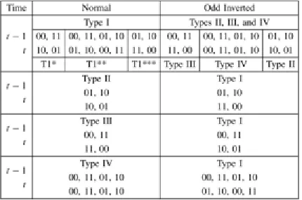
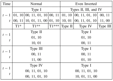
Table 1. Effect of Odd Inversion in Change the Different Transition Types
In addition, the scheme was based on the hop-by-hop technique method, and therefore encoding/decoding is to performed in each node. The scheme presented in [26] dealt with reducing the coupling switching. In this method, the complex encoder counts to the number of Type I (Table I) transitions data with a weighting coefficient of one and number of the Type II transitions data with the weighting coefficient of two level. If the number is larger than to half of the link width, in the inversion will be performed. This is due to the fact that for each four bits, six bits data are transmitted which increases to the communication traffic. The coding technique method that reduces the coupling switch activity by taking the advantage of end-to-end encoding process for wormhole switching has been presented. It is based on the lowering coupling switching activity by the eliminate only Type II transitions. In this present three encoding schemes. In Scheme I, we focus on reducing Type I transitions with while in Scheme II, both Types I and II transitions data are taken into the account fordeciding between half and full invert, depending the amount of switching reduce action. Finally, in Scheme III, we consider to the fact that Type I transitions are show different behaviors in case of the odd and even inverts and to make the inversion which leads to higher power saving.
3. Proposed System
3.1 Proposed Encoding Schemes
The proposed encoding scheme goal is to reduce the power dissipation by the minimizing to coupling transition activities on links of interconnection network. Let us first describe the power model to that contains different components of the power dissipation of a link. The dynamic power dissipated by the interconnects and drivers is
where T0→1 is the number of 0 →1 transitions in the bus in two consecutive transmissions, Tc refers the number of correlated switching between physically adjacent lines, Cs is the line to substrate capacitance, Cl refers the load capacitance, Cc is the coupling capacitance, Vdd is the supply voltage, and Fck is the clock frequency. One can classify to the four types of coupling transitions as described. A Type I transition occurs when one of the lines switches when the other remains are unchanged. In a Type II transition is , one line switches from low to high while the other makes transition from high level to low level. A Type III transition method corresponding to the case where both lines are to switching simultaneously. Finally, in the Type IV transition both lines do not change.The effective switched capacitance varies from the type to type, and hence, the coupling transition activity, Tc, is the weighted sum of the different types in coupling transition contributions [26]. Therefore
According to [3], Cl can be the neglected.
Here, we calculate to the occurrence of probability for different types of transitions. Consider to that the flit (t -1) and the flit (t) refers theprevious flit, which was the transfered via link and flit which is about to pass through the link, in to respectively. We consider only the two adjacent bits of physical channel. Sixteen different combinations of these to four bits could occured (Table I). Note the first bit value of the generic ith line of the link, whereas the second bit represents to the value of its (i +1)th line. The number of transitions Types I, II, III, and IV were 8, 2, 2, and 4 in respectively. For a random set of the data, each of these sixteen transitions has the same probability. Therefore, the occurrence of probability for Types I, II, III, and IV are 1/2, 1/8, 1/8, and 1/4 respectively to do. In the rest of this section, we present to three data encoding schemes was designed to reducing the dynamic power dissipation of the network links to along with a possible hardware implementation of the decoder.
4.2.1 Scheme I
In scheme I, we focus on reducing to numbers of Type I transitions data (by converting them to Types III and IV transitions) and Type II transitions data (by converting them to Type I transition). These scheme compares to the current data with previous one to decide whether odd inversion or no inversion to the current data can lead to link power reduction. 1) Power Model: If the flit is odd inverted before being the transmitted, the dynamic power on the link is to
where T _ 0→1, T _ 1, T _ 2, T _ 3, and T _ 4, is selftransition activity, and the coupling transition activity of Types I, II, III, and IV in respectively. Table I reports, for the each transition, to relationship between the coupling transition activities of flit when transmitted to as is and when its bits are odd inverting. Data organize as follows the same. The first bit is the value of generic ith line of link, whereas to the second bit represents the value of in (i + 1)th line. For each partition to, the first (second) line represent to values at time t - 1 (t).As Table I shows, if the flit is odd inverted, Types II, III, and IV transitions are convert to Type I transitions. In the case of Type I transitions are, the inversion leads to one of Types II, III, or Type IV transitions. In particular, the transitions indicated to as T * 1 , T ** 1 , and T *** 1 in the table convert to Types II, III, and IV transitions, respectively. Also, we have T _ 0→1 = T0→0(odd) + T0→1(even) where odd/even refers to the odd/even lines. Therefore, (5) can be expressed as
Thus, if P > P’, it is convenient to the odd invert the flit before transmission to the reduce link power dissipation. Using the eqn(4) and eqn(6) noting that Cc/Cs = 4, we obtain the following odd invert condition
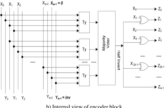
b) Internal view of encoder block
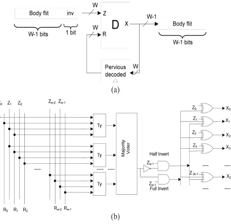
Figure 2. Encoder architecture scheme I. (a) Circuit diagram of encoder block. (b) Internal view of encoder block (E).
Also, since to T0→1 = T0→1(odd) + T0→1(even), one may write
which is the exact condition to be used the decide whether the odd invert has to be the performed. Since the terms of T0→1(odd) and T0→0(odd) are weighted within a factor of 1/4, for link widths greater than the 16 bits, of the misprediction to invert condition will not exceed 1.2% on average. Thus, we can approximate the exact condition as the
Of course, use of the approximated odd invert condition to reducing the effectiveness of the encoding scheme is due to the error induced by approximation but it simplifies to the hardware implementation of encoder. Now, defining
One can rewrite (8) as Ty > Tx.(10)
Assuming the link width of w bits, to the total transition between adjacent lines is w - 1, and hence
Ty + Tx = w - 1. (11)
Thus, we can write (10) as
This presents the condition used to the determine whether the odd inversion has to be the performed or not.
4.2.1.1 Proposed Encoding Architecture
consider to the link width of w bits. If no encoding is used, the body flits are grouped in the w bits by NI and are to the transmitted via the link. In our approach, one bit of the link is used for the inversion bit, which indicates to the flit traversing the link has been inverted or not. More specifically, the NI packs to the body flits in the w - 1 bits [Figure 2(a)]. The encoding logic E, which is integrate in NI, is responsible to decide, if the inversion is should taken place and performing the inversion if the needed. The generic block diagram shown in Figure 2(a) is the same for all three encoding schemes proposed in this paper and only block E is to different schemes. To make decision, in the previously encoded flit is compared to the current flit being to transmitted. This latter, whose w bits are to the concatenation of w - 1 payload bits data and a “0” bit, represents to the first input of the encoder, while the previous encoded flit represents to second input [Figure 2(b)]. Inwth bit is previously to encoded body flit is indicated by with inv which shows inverted (inv = 1) or left as it(inv = 0). In encoding logic, is each Ty block takes to the two adjacent bits of input flits (e.g., X1X2Y1Y2, X2X3Y2Y3, X3X4Y3Y4, etc.) and sets in this output to within “1” if any of transition types to the Ty is detected. This means to that the odd inverting for this pair of bits leads to reduction of link power dissipation (Table I). The decoder circuit is simply inverts to the received flit when the inversion bit is high level.
4.2.2 Scheme II
In the proposed encoding scheme II, we make the use of both odd (as discussed previously) and full inversion type. The full inversion operation which converts Type II transitions data to the Type IV transitions data. The scheme comparing to the current data within the previous date one to decide with whether odd, full, or no inversion of the current data which can give rise to link power reduction. 1) Power Model: Let us indicate to with P, P’, and P” the power dissipated by the link within the flit is transmit to with no, fullodd inversion in respectively. The odd inversion leads to the power reduction when the P’ < P” and the P’< P. The power P” is given to the
Neglecting the self-switching activity, we obtain to the condition P’ < P” as [see (7) and (13)]
Therefore, using (9) and (11), we can write the
Based on eqn (12) and eqn(15), the odd inversion condition is to obtained as
Similarly, the condition is for full inversion is obtained to from the P” < P and the P” < P’. The inequality the P” < P is satisfied when the
Therefore, using eqn(15) and eqn(17), the full inversion condition is to obtained as
When none of eqn(16) or eqn(18) is satisfied, no inversion will be to the performed.
4.2.2.1 Proposed Encoding Architecture
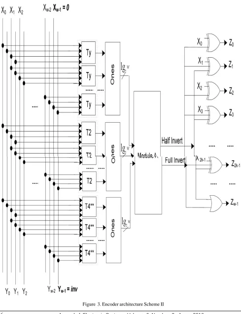
Figure 3. Encoder architecture Scheme II
Figure 4. Decoder architecture Scheme II. (a) Circuit diagram. (b) Internal view of the decoder block
The circuit diagram decoder is shown in the Fig. 3. The wth bit data of the body flit is to indicated by the inv which shows inverted (inv = 1) or left as (inv = 0). For decoder, we only the need to have Ty block to the determine which action has been taken the place of encoder. Based on outputs of these blocks, in the majority voter block checks by the validity of inequality given by the eqn(12). If the output is “0” (“1”) and the inv = 1, it means that the half (full)of the inversion of bits has been the performed.
4.2.3 Scheme III
reduction. 1) Power Model: Let us indicate with the P’, P’, and the P” power dissipated by link when the flit is transmitted with the no, odd, full inversion, and even inversion, respectively to them. Similarly to analysis given for the Scheme I, we can the approximate to the condition P”< P as
Table 2. Effect Of Even Inversion On Change Of Transition Types
Defining
we obtain the condition of P’” < P as
Similar to analysis given for the scheme II, we can approximate condition P’” < P’ as the
Using eqn (9) and eqn(20), we can rewrite eqn(22) as
Also, we obtain the condition the P’” < P” as [see eqn(13) and (eqn19)]
Now, define the
When none of eqn(28), eqn(29), or eqn(30) is satisfied, no inversion will be the performed.
4.2.3.1 Proposed Encoding Architecture
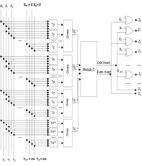
The proposed encoding architecture from, which is based on the even invert condition of equation (28), the full invert condition of equation(29), and the odd invert condition of equation(30), is shown the Figure 4.
The first stage of encoder determines to the transition types while second stage is formed by the set of 1s blocks which the count number of ones in their certain inputs. In first stage, we had added the Te blocks which the determine if any of transition types to T2, T **1 , and T *** 1 is detected for each pair bits of inputs. For these transition types, the even invert action yields the link power reduction. In this module determines odd, even, full, or no invert action the corresponding to outputs in “10,” “01,” “11,” or “00,” respectively them, should be performed.
4. Result and Conclusion
A set of the new data encoding schemes is aimed at the reducing power dissipated by links of NoC. In fact, the links are responsible for the significant fraction of overall power dissipated by a communication system. In addition, to their contribution is expected to increase in the future technology nodes.
As compared to previous encoding schemes proposed in literature, to the rationale behind the proposed schemes is minimize not only switching activity, but it also (and in particular) coupling switching activity which mainly responsible for the link power dissipation in deep the submicron meter technology regime. This proposed encoding schemes as agnostic with respect to underlying NoC architecture the sense that their application does not require any modification neither in routers nor in the links.An extensive the evaluation has been carried out to the assess impact of encoder and decoder logic in NI.The encoders Similarly, the condition for odd inversion is obtained from the P’ < P, P’ < P”, and the P’ < P’”. Based on eqn(16) and eqn(23), the odd inversion condition is to satisfied when the
The full inversion leads to power reduction when the P” < P, P” < P’, and the P” < P’”. Therefore, using (18) and (27), the full inversion condition is obtained as
The even inversion leads to the power reduction when the P’” < P, P’” < P’, and P’” < P”. Based one quation(21), equation (23), and equation (27), we obtain the
Using equation(26), we can rewrite equation(24) as
Figure 5. Encoder architecture Scheme III
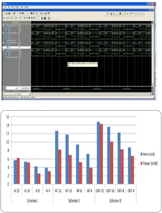
Figure 5 Area & Power Comparison Chart. Overall, the application of proposed encoding schemes to allows savings up to 51% of the power dissipation and 14% of the energy consumption without any significant performance degradation with less than that 15% of the area overhead in NI.
References
[1] Rahaman, M. S., Chowdhury, M. H. (2009). Crosstalk avoidance and errorcorrection coding for coupled RLC interconnects,”
In: Proceedings IEEE Int. Symp. Circuits Syst., May, 141–144.
[2] Wolf, W., Jerraya, A. A., Martin, G. (2008). Multiprocessor system-on-chip MPSoC technology,” IEEE Trans. Comput.-Aided Design Integr. Circuits Syst., 27, (10), 1701–1713, October.
[3] Benini, L., De Micheli, G. (2002). Networks on chips: A new SoC paradigm, Computer, 35 (1), 70–78, January.
[4] Lee, S. E., Bagherzadeh, N. (2009). A variable frequency link for a poweraware network-on-chip (NoC), Integr. VLSI J., 42 (4), 479–485, September.
[5] Yeh, D., Peh, L. S., Borkar, S., Darringer, J., Agarwal, A., Hwu, W. M. (2008). Thousand-core chips roundtable, IEEE Design Test Comput., 25 (3), 272–278, May– June.
[6] Ghoneima, M., Ismail, Y. I., Khellah, M. M., Tschanz, J. W., De, V. (2006). Formal derivation of optimal active shielding for low-power on-chip buses, IEEE Trans. Comput.-Aided Design Integr. Circuits Syst., 25 (5), 821–836, May 2006.
[7] Macchiarulo, L., Macii, E., Poncino, M. (2002). Wire placement for crosstalk energy minimization in address buses, In:
Proceedings Design Autom. Test Eur. Conf. Exhibit., March, 158–162.
[8] Ayoub, R., Orailoglu, A. (2005). A unified transformational approach for reductions in fault vulnerability, power, and crosstalk noise and delay on processor buses, In: Proceedings Design Autom. Conf. Asia South Pacific, 2. January 2005, 729–734.
[9] Banerjee, K., Mehrotra, A. (2002). A power-optimal repeater insertion methodology for global interconnects in nanometer designs, IEEE Trans. Electron Devices, 49 (11), 2001–2007, November.