Advances in Radio Science, 3, 281–285, 2005 SRef-ID: 1684-9973/ars/2005-3-281
© Copernicus GmbH 2005
Advances in
Radio Science
Gate Leakage Reduction by Clocked Power Supply of Adiabatic
Logic Circuits
Ph. Teichmann, J. Fischer, E. Amirante, St. Henzler, A. Bargagli-Stoffi, Ch. Otte, and D. Schmitt-Landsiedel
Lehrstuhl f¨ur Technische Elektronik, Technische Universit¨at M¨unchen, Theresienstrasse 90, D-80290 Munich, Germany
Abstract. Losses due to gate-leakage-currents become more
dominant in new technologies as gate leakage currents in-crease exponentially with decreasing gate oxide thickness. The most promising Adiabatic Logic (AL) families use a clocked power supply with four states. Hence, the fullVDD
voltage drops over an AL gate only for a quarter of the clock cycle, causing a full gate leakage only for a quarter of the clock period. The rising and falling ramps of the clocked power supply lead to an additional energy consumption by gate leakage. This energy is smaller than the fraction caused by the constantVDD drop, because the gate leakage
expo-nentially depends on the voltage across the oxide. To ob-tain smaller energy consumption, Improved Adiabatic Logic (IAL) has been introduced. IAL swaps all n- and p-channel transistors. The logic blocks are built of p-channel devices which show gate tunneling currents significantly smaller than in n-channel devices. Using IAL instead of conventional AL allows an additional reduction of the energy consump-tion caused by gate leakage. Simulaconsump-tions based on a 90nm CMOS process show a lowering in gate leakage energy con-sumption for AL by a factor of 1.5 compared to static CMOS. For IAL the factor is up to 4. The achievable reduction varies depending on the considered AL family and the complexity of the gate.
1 Introduction
Future applications raise the needs for computing complex-ity. Device scaling increases the integration density, but with smaller devices and thinner gate oxides, leakage cur-rents are not neglectable any longer and leakage reduction methods are of concern in modern CMOS design methodolo-gies. Many proposals have been presented to supress leakage currents in static CMOS, e.g. Henzler et al. (2004, 2005); Drazdziulis et al. (2003); Narenda et al. (2001); Hamazoglu et al. (2002).
Adiabatic Logic is a promising low power circuit method to reduce the energy dissipation in digital logic, by using a constant current to efficiently charge a capacity. Therefore, a
Correspondence to: Ph. Teichmann
teichmann@tum.de
clocked power supply (power clock) is used, that consists of four states. Only during one of the four states the whole sup-ply voltageVDDdrops across the gate. Hence a reduction of
the leakage currents is implemented explicitely by the power clock in AL circuits.
In this paper the reduction of gate leakage currents through the power clock is investigated. The following Sect. 2 gives a short overview of the physical principles of gate leakage. Section 3 deals with the adiabatic power clock leading to an estimation of the savings in gate leakage in Sect. 4. A single MOS device is taken into account, driven by a constant sup-ply voltage on the one hand and the dynamic power clock of an adiabatic system on the other hand. Section 5 presents the results of simulations in a 90 nm CMOS technology. Three different adiabatic logic topologies are simulated and com-pared to an implementation in static CMOS.
2 Gate leakage
In state of the art devices with oxide thicknesses below 2 nm, gate leakage currents become a noticable part of static energy dissipation. Depending on the voltage from gate to substrate, gate tunneling can be divided into two parts. One is called Fowler-Nordheim tunneling (FNT) and the other is called di-rect tunneling (DT). FNT occurs, when the charges tunnel through a triangular potential barrier. Hence, a high voltage is needed in order to gain FNT. In normal device operation only DT results in a significant gate leakage current value. For an n-channel device, the electrons tunnel from the con-duction band of the substrate through a trapezoidal oxide po-tential barrier (see Fig. 1). The equation describing the DT current density is given by Schuegraf et al. (1994).
JDT =AEox2 exp
−Bh1−(1−Vox
φox)
3/2i
Eox
(1)
A=q3/16π2hφ¯ ox (2)
B=4 √
2m∗φ3/2
ox /3hq ,¯ (3)
whereφox is the barrier height. Asφox for holes in the
E
E
CE
FDT
Fig. 1. Direct tunneling of electrons from the conduction band of
the substrate into the conduction band of the polysilicon. The elec-trons tunnel through a trapezoidal oxide potential barrier.
in the conduction band, the gate leakage current in n-MOS devices is higher than the gate leakage current in a p-MOS device. From simulations with parameters of a 90 nm tech-nology we obtained gate leakage currents in n-MOS devices that are about 10 times higher than in a p-MOS device. This leads to the assumption, that designs using predominantly p-channel devices suffer less from gate leakage than those using n-channel devices.
3 Adiabatic power clock
Adiabatic logic families suitable for building digital systems use a power clock consisting of four phases (see Fig. 2). A phase is separated into four states (Fig. 3a) named Evaluate
E), Hold (H), Recover (R) and Wait (W). The duration of
each state isT /4, whereT is the period of the clock cycle. During E the internal nodes of the AL gate are charged de-pending on the outputs of the preceding gate. The outputs of the gate are valid during H. Charge is recovered from the internal nodes to the oscillator in the R state. For symmetry reasons and thus easier generation of the waveform, the state
W has been introduced.
The gates are connected to the power clock in such a way, that if a gate is in E state, its preceding gate is in H state. In Fig. 2 the way data is transferred is symbolized by the arrows. So the gate connected to phaseφ1 evaluates the inputs that are deliverd by the preceding gate at phaseφ0. Looking at the power clock, the full supply voltage drops at the gate for just a quarter of a cycle. During E and R the voltage is ramped from 0 toVDDand vice versa, leading to
a leakage power dissipation as well. Compared to a static CMOS gate, where the supply voltageVDD is constant the
whole time, a reduction in static power dissipation through gate leakage is expected. Figure 3b shows the gate leakage current for a phase of the adiabatic power clock and it’s static CMOS counterpart.
4 Estimation of the savings through adiabatic power clock
For a prediction of the savings through the adiabatic power clock compared to static CMOS using a constant
t
Φ2
t
Φ3
t t
Φ1
Fig. 2. The power clock for the considered adiabatic logic families.
It consists of four phases. The arrows show, when data is transferred from one gate to the consecutive gate.
VDD supply, a single MOSFET device is characterized
here. Therefore, the gate leakage energy dissipation factor (GLEDF)ηbetween the energy dissipation caused by gate leakage for the different arrangements in Fig. 4 is introduced. η= Egl,CMOS
Egl,AL
(4) Taking Eq. (1) and the waveformu(t ) of a power clock phase, we can calculateηas follows.
η= R
TVDDJDT(VDD)dt R
Tu(t )JDT(u(t ))dt
= VDDJDT(VDD)T
2R0T /4u(t )JDT(u(t ))dt+R0T /4VDDJDT(VDD)dt
(5)
η= JDT(VDD)T
8 T
RT /4
0 t JDT(u(t ))dt+T4JDT(VDD)
η−1=
8 T
RT /4
0 t JDT(u(t ))dt JDT(VDD)T
+1
4 (6)
Looking atηin Eq. (6) we see two terms in the denom-inator. The first term represents the dissipation of energy due to gate leakage during the ramps E and R of the power clock phase, the second term arises from the constantVDD
drop during H state of the power clock phase. Neglecting the first term in the denomiator, the energy dissipation fac-torηwould obviously be four. Considering the whole equa-tion and assuming a linear dependence of the gate leakage current on the voltage across the oxide,ηwould be as low as two. From Eq. (1) the gate leakage current is exponen-tially dependent on the voltage across the oxide, resulting in a lower gate leakage than in case of a linear dependence. So the expected value will be in betweenη=2 andη=4.
The GLEDF is dependent on the supply voltageVDD. If
Ph. Teichmann et al.: Gate Leakage Reduction by Clocked Power Supply of Adiabatic Logic Circuits 283
Book: Kleinheubacher Berichte
MS No.: KH2004-A-00014
First author: Philip Teichmann 3
Looking at the power clock, the full supply voltage drops at the gate for just a quarter of a cycle. During E and R the voltage is ramped from0toVDDand vice versa, leading to a leakage power dissipation as well. Compared to a static CMOS gate, where the supply voltageVDDis constant the whole time, a reduction in static power dissipation through gate leakage is expected. Figure 3.b) shows the gate leakage current for a phase of the adiabatic power clock and it’s static CMOS counterpart.
a)
T
E
H
R
W
t
u(t)
b) igl,AL igl,CMOS Φ i t tFigure 3. a) A phase of the adiabatic power clock is separated into four states. b) Respective gate leakage current at a single transistor.
4
Estimation of the savings through adiabatic power clock
For a prediction of the savings through the adiabatic power clock compared to static CMOS using a constantVDDsupply, a single MOSFET device is characterized here. Therefore, the gate leakage energy dissipation factor (GLEDF)ηbetween the energy dissipation caused by gate leakage for the different arrangements in figure 4 is introduced.
V
DDFigure 4. The estimation for the savings is performed on a single transistor. On the left one can see the circuit in case of static CMOS and on the right
the circuit for the clocked power supply of an adiabatic system.
η=Egl,CM OS
Egl,AL
(4)
Taking equation (1) and the waveformu(t)of a power clock phase, we can calculateηas follows.
η =
R
T
VDDJDT(VDD)dt R
T
u(t)JDT(u(t))dt
= VDDJDT(VDD)T
2 T /R4
0
u(t)JDT(u(t))dt+ T /R4
0
VDDJDT(VDD)dt
(5)
η = JDT(VDD)T 8
T T /R4
0
tJDT(u(t))dt+T4JDT(VDD)
η−1= 8
T T /R4
0
tJDT(u(t))dt
JDT(VDD)T +1
4 (6)
Looking atηin equation (6) we see two terms in the denominator. The first term represents the dissipation of energy due to gate leakage during the ramps E and R of the power clock phase, the second term arises from the constantVDD drop during H state of the power clock phase. Neglecting the first term in the denomiator, the energy dissipation factorη
would obviously be four. Considering the whole equation and assuming a linear dependence of the gate leakage current on the voltage across the oxide,ηwould be as low as two. From equation (1) the gate leakage current is exponentially dependent on the voltage across the oxide, resulting in a lower gate leakage than in case of a linear dependence. So the expected value will be in betweenη= 2andη= 4.
The GLEDF is dependent on the supply voltageVDD. If we have a look at the inverse GLEDFη−1 we see, that the
Fig. 3. (a) A phase of the adiabatic power clock is separated into four states. (b) Respective gate leakage current at a single transistor.
Book: Kleinheubacher Berichte
MS No.: KH2004-A-00014
First author: Philip Teichmann 3
Looking at the power clock, the full supply voltage drops at the gate for just a quarter of a cycle. During E and R the voltage is ramped from0toVDDand vice versa, leading to a leakage power dissipation as well. Compared to a static CMOS gate, where the supply voltageVDDis constant the whole time, a reduction in static power dissipation through gate leakage is expected. Figure 3.b) shows the gate leakage current for a phase of the adiabatic power clock and it’s static CMOS counterpart.
a)
T
E
H
R
W
t
u(t)
b) igl,AL igl,CMOS Φ i t tFigure 3. a) A phase of the adiabatic power clock is separated into four states. b) Respective gate leakage current at a single transistor.
4 Estimation of the savings through adiabatic power clock
For a prediction of the savings through the adiabatic power clock compared to static CMOS using a constantVDDsupply, a single MOSFET device is characterized here. Therefore, the gate leakage energy dissipation factor (GLEDF)ηbetween the energy dissipation caused by gate leakage for the different arrangements in figure 4 is introduced.
V
DDFigure 4. The estimation for the savings is performed on a single transistor. On the left one can see the circuit in case of static CMOS and on the right
the circuit for the clocked power supply of an adiabatic system.
η=Egl,CM OS
Egl,AL (4)
Taking equation (1) and the waveformu(t)of a power clock phase, we can calculateηas follows.
η =
R
T
VDDJDT(VDD)dt R
T
u(t)JDT(u(t))dt
= VDDJDT(VDD)T
2 T /R4
0
u(t)JDT(u(t))dt+ T /R4
0
VDDJDT(VDD)dt
(5)
η = JDT(VDD)T 8
T T /R4
0
tJDT(u(t))dt+T4JDT(VDD)
η−1= 8
T T /R4
0
tJDT(u(t))dt
JDT(VDD)T + 1
4 (6)
Looking atηin equation (6) we see two terms in the denominator. The first term represents the dissipation of energy due to gate leakage during the ramps E and R of the power clock phase, the second term arises from the constantVDD drop during H state of the power clock phase. Neglecting the first term in the denomiator, the energy dissipation factorη would obviously be four. Considering the whole equation and assuming a linear dependence of the gate leakage current on the voltage across the oxide,ηwould be as low as two. From equation (1) the gate leakage current is exponentially dependent on the voltage across the oxide, resulting in a lower gate leakage than in case of a linear dependence. So the expected value will be in betweenη= 2andη= 4.
The GLEDF is dependent on the supply voltageVDD. If we have a look at the inverse GLEDFη−1we see, that the Fig. 4. The estimation for the savings is performed on a single
tran-sistor. On the left one can see the circuit in case of static CMOS and on the right the circuit for the clocked power supply of an adiabatic system.
η−1comes from the integration over the gate leakage power during the H state. For higher values ofVDD, the integral of
the power during the ramps becomes less remarkable com-pared to the integral over the gate leakage power during the
H state.
A Matlab simulation was performed to calculate the fac-torη. The parameters for modeling the gate leakage current according to equation (1) were taken from a 90 nm CMOS technology. As expected, the results in Fig. 5 show, thatηis dependent on the supply voltage. Higher supply voltages re-sult in a higher reduction of gate leakage currents in adiabatic logic compared to static CMOS.
The factor ηis an estimation for the savings at a single transistor. For each logic family the topologies and the logic functions have to be taken into account. The Efficient Charge Recovery Logic (ECRL) (Moon et al., 1996) consists of a pair of cross-coupled p-channel devices (Fig. 6a). The logic function blocksF andF are connected between the outputs of the gate and GND. The Positive Feedback Adiabatic Logic (PFAL) (Fig. 6b) uses a latch as basic cell with the function blocks connected from power clock to the outputs of the gate. These two families use logic function blocks consisting of n-channel devices. To additionally reduce the adiabatic losses the Improved PFAL (IPFAL) family (Fig. 6c) has been intro-duced (Fischer et al., 2003). IPFAL, like PFAL, consists of a cross-coupled latch but the logic blocks are implemented with p-channel devices only. This is advantageous, because gate leakage currents – as mentioned in Sect. 2 – are almost a decade lower in p-channel devices. But all three families have in common, that an inverter cell uses at least twice as many MOSFET devices as the corresponding CMOS gate. Hence, the factor of the estimation is influenced by the logic family and the implemented logic function. A device quan-tity factor (DQF)f nfor the relation of the count of n-channel
Book: Kleinheubacher Berichte
MS No.: KH2004-A-00014
First author: Philip Teichmann 4
numerator in the first term is the integral over the gate leakage power at the ramps. The denominator in the equation for
η−1comes from the integration over the gate leakage power during the H state. For higher values ofV
DD, the integral of the power during the ramps becomes less remarkable compared to the integral over the gate leakage power during the
H state.
A Matlab simulation was performed to calculate the factor η. The parameters for modeling the gate leakage current
according to equation (1) were taken from a 90nm CMOS technology. As expected, the results in figure 5 show, thatηis
dependent on the supply voltage. Higher supply voltages result in a higher reduction of gate leakage currents in adiabatic logic compared to static CMOS.
0 0.5 1 1.5 2 2.6 2.7 2.8 2.9 3 3.1
VGS[V]
η
Figure 5. A Matlab simulation of equation (6) using parameters of a 90nm CMOS technology. The energy dissipation factorηis dependent on the supply voltage.
The factorηis an estimation for the savings at a single transistor. For each logic family the topologies and the logic
functions have to be taken into account. The Efficient Charge Recovery Logic (ECRL) [Moon et. al. (1996)] consists
of a pair of cross-coupled p-channel devices (figure 6.a)). The logic function blocksF andF are connected between
the outputs of the gate and GND. The Positive Feedback Adiabatic Logic (PFAL) (figure 6.b)) uses a latch as basic cell with the function blocks connected from power clock to the outputs of the gate. These two families use logic function blocks consisting of n-channel devices. To additionally reduce the adiabatic losses the Improved PFAL (IPFAL) family (figure 6.c)) has been introduced [Fischer et. al. (2003)]. IPFAL, like PFAL, consists of a cross-coupled latch but the logic blocks are implemented with p-channel devices only. This is advantageous, because gate leakage currents - as mentioned in section 2- are almost a decade lower in p-channel devices. But all three families have in common, that an inverter cell uses at least twice as many MOSFET devices as the corresponding CMOS gate. Hence, the factor of the estimation is
influenced by the logic family and the implemented logic function. A device quantity factor (DQF)f nfor the relation
of the count of n-channel devices is defined. The p-channel devices are neglected, because the gate leakage currents are almost a decade lower than in n-channel MOSFETS.
f n= nAL
nCM OS
= transistorcountn,AL
transistorcountn,CM OS (7)
Three logic functions are investigated. An inverter (INV), a NAND and a function called LOGIC5. LOGIC5 is a five
input logic, where the logic function treesFandFare balanced, i. e. the number of parallel and serial devices is equal in
the two logic function blocks. The count of n-channel devices and the corresponding factorf nfor the investigated logic
functions are listed in table 1.
a) nMOS
F
nMOSF
in1 inN out out in1 inbN b) F F in1 inN out out in1 inN c) VDD F in1inN F inN
in1 out out
Figure 6. Schematics of a) ECRL, b) PFAL and c) IPFAL cell. The logic function blocks consist of p-channel devices for IPFAL and n-channel devices otherwise.
Fig. 5. A Matlab simulation of equation (6) using parameters of a
90 nm CMOS technology. The energy dissipation factorηis depen-dent on the supply voltage.
devices is defined. The p-channel devices are neglected, be-cause the gate leakage currents are almost a decade lower than in n-channel MOSFETS.
f n= nAL nCMOS
= t ransist orcountn,AL t ransist orcountn,CMOS
(7) Three logic functions are investigated. An inverter (INV), a NAND and a function called LOGIC5. LOGIC5 is a five input logic, where the logic function treesF andF are bal-anced, i.e. the number of parallel and serial devices is equal in the two logic function blocks. The count of n-channel de-vices and the corresponding factor f nfor the investigated logic functions are listed in Table 1.
284 Ph. Teichmann et al.: Gate Leakage Reduction by Clocked Power Supply of Adiabatic Logic Circuits
Table 1. Transistor counts and DQF (f n) of the investigated logic families and functions.
nCMOS nECRL nP F AL nI P F AL f nECRL f nP F AL f nI P F AL
INV 1 2 4 2 2 4 2
NAND 2 4 6 2 2 3 1
LOGIC5 5 10 12 2 2 2.4 0.4
First author: Philip Teichmann 4
numerator in the first term is the integral over the gate leakage power at the ramps. The denominator in the equation for
η−1comes from the integration over the gate leakage power during the H state. For higher values ofV
DD, the integral
of the power during the ramps becomes less remarkable compared to the integral over the gate leakage power during the
H state.
A Matlab simulation was performed to calculate the factorη. The parameters for modeling the gate leakage current according to equation (1) were taken from a 90nm CMOS technology. As expected, the results in figure 5 show, thatηis dependent on the supply voltage. Higher supply voltages result in a higher reduction of gate leakage currents in adiabatic logic compared to static CMOS.
0 0.5 1 1.5 2 2.6
2.7 2.8 2.9 3 3.1
V
GS[V]
η
Figure 5. A Matlab simulation of equation (6) using parameters of a 90nm CMOS technology. The energy dissipation factorηis dependent on the
supply voltage.
The factorηis an estimation for the savings at a single transistor. For each logic family the topologies and the logic functions have to be taken into account. The Efficient Charge Recovery Logic (ECRL) [Moon et. al. (1996)] consists of a pair of cross-coupled p-channel devices (figure 6.a)). The logic function blocksF andF are connected between the outputs of the gate and GND. The Positive Feedback Adiabatic Logic (PFAL) (figure 6.b)) uses a latch as basic cell with the function blocks connected from power clock to the outputs of the gate. These two families use logic function blocks consisting of n-channel devices. To additionally reduce the adiabatic losses the Improved PFAL (IPFAL) family (figure 6.c)) has been introduced [Fischer et. al. (2003)]. IPFAL, like PFAL, consists of a cross-coupled latch but the logic blocks are implemented with p-channel devices only. This is advantageous, because gate leakage currents - as mentioned in section 2- are almost a decade lower in p-channel devices. But all three families have in common, that an inverter cell uses at least twice as many MOSFET devices as the corresponding CMOS gate. Hence, the factor of the estimation is influenced by the logic family and the implemented logic function. A device quantity factor (DQF)f nfor the relation of the count of n-channel devices is defined. The p-channel devices are neglected, because the gate leakage currents are almost a decade lower than in n-channel MOSFETS.
f n= nAL
nCM OS
= transistorcountn,AL
transistorcountn,CM OS
(7) Three logic functions are investigated. An inverter (INV), a NAND and a function called LOGIC5. LOGIC5 is a five input logic, where the logic function treesF andF are balanced, i. e. the number of parallel and serial devices is equal in the two logic function blocks. The count of n-channel devices and the corresponding factorf nfor the investigated logic functions are listed in table 1.
a)
nMOS
F
nMOS
F
in1
inN
out out
in1
inbN
b)
F F
in1
inN
out out
in1
inN
c)
VDD
F
in1
inN F inN
in1 out out
Figure 6. Schematics of a) ECRL, b) PFAL and c) IPFAL cell. The logic function blocks consist of p-channel devices for IPFAL and n-channel devices otherwise.
Fig. 6. Schematics of (a) ECRL, (b) PFAL and (c) IPFAL cell. The logic function blocks consist of p-channel devices for IPFAL and
n-channel devices otherwise.
Table 2. Effective gate leakage energy dissipation factor (effective
GLEDF) at a supply voltage of 0.8V.
ηeff@0.8V ECRL PFAL IPFAL
INV 1.43 0.715 1.43
NAND 1.43 0.95 2.86
LOGIC5 1.43 1.19 7.15
With the knowledge off nan effective GLEDFηeff can
be calculated.
ηeff = η
f n (8)
With Eq. (8) the factor η, obtained from the estimation of a single device, is adapted to the used logic family and the implemented logic function.
The arrangement of the devices in the logic function has an influence on the gate leakage induced energy dissipation. Additionally for PFAL another fact reduces the gate leakage caused by the input transistors. If the voltage of a PFAL inverter input transistor is VDD, the phase is connected to
drain and source of the input device, leading to decreasing voltagesVGS andVGD. Hence, the gate leakage is reduced
with the rising voltage of the phase. As the DQF contains no information about the arrangement of the devices inside the logic function blocks,ηeff is a rough estimation.
The effective GLEDFηeff can be calculated with the
fac-torη. For the supply voltage of 0.8 V,ηis 2.86 (see Fig. 5). With that,ηeff@0.8 V can be calculated using the
informa-tion onf nprinted in Table 1, leading to Table 2.
5 Simulation results
Looking at the simulation arrangement of the INV function in Fig. 7, a chain of five gates is used for the simulation. Fig-ure 7 shows the scheme of the simulation arrangement. The gates S1 and S2 are used to provide a realistic input signal at the device under test S3. The gates S4 and S5 are used to pro-vide a realistic load. The chain is terminated with capacities of 0.1 fF. The transistor model is BSIM4 with parameters of an industrial 90 nm CMOS technology. The supply voltage is 0.8 V.
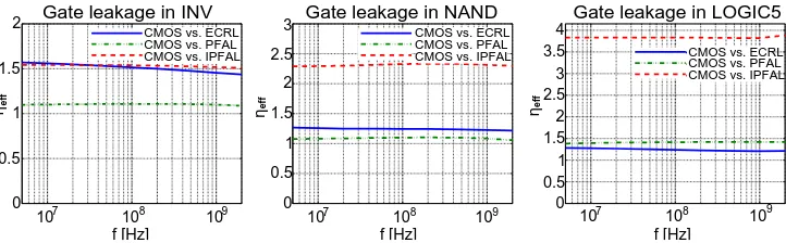
The simulation results are shown in Fig. 8. The effective GLEDFηeff is plotted against the frequency. First we take a
look at the influence of the logic functions onηeff for each
adiabatic family.
ECRL has approximately the same value for all logic func-tions. For the INV function, ECRL reaches a factorηeff=1.5.
Looking at the simulation results for the NAND function one can see, that the simulated value is worse than the predic-tion. This comes from the fact, that parallel connected de-vices cause more gate leakage than serial connected dede-vices. The ECRL and the CMOS NAND contain a serial connection of two n-channel devices. Additionally, the ECRL NAND includes a parallel connection of n-channel devices in theF block. In fact, the different gate leakage for serial and par-allel connected devices is not considered in the estimation, leading to a deviation from the predicted value. For PFAL the factorηeff increases for functions with more inputs, as the
overhead due to the two additional n-MOSFETs inside the latch becomes less important. The advantageous location of the logic blocks in PFAL result in a higherηeff for LOGIC5
for PFAL (ηeff≈1.4), compared to ECRL (ηeff≈1.3). PFAL
reaches its maximum ofηeff for functions with higher input
Ph. Teichmann et al.: Gate Leakage Reduction by Clocked Power Supply of Adiabatic Logic Circuits 285
Book: Kleinheubacher Berichte
MS No.: KH2004-A-00014
First author: Philip Teichmann 5
nCM OS nECRL nP F AL nIP F AL f nECRL f nP F AL f nIP F AL
INV 1 2 4 2 2 4 2
NAND 2 4 6 2 2 3 1
LOGIC5 5 10 12 2 2 2.4 0.4
Table 1. Transistor counts and DQF (f n) of the investigated logic families and functions.
ECRL uses n-channel devices for its logic blocks, so the factorf nstays 2, independent of the implemented logic function. For PFAL, the INV uses 4 n-MOSFETs. Two as input transistors in the logic function blocks, and two more in the latch. The CMOS inverter just uses one n-channel device. Hence, the two additional n-channel devices in the latch of a PFAL gate result in a drastic overhead for logic functions with few input signals (e. g. INV, NAND, NOR). But for PFAL gates with a higher input signal count, the overhead caused by the two additional devices in the latch is smaller. For the LOGIC5 gate, the factorf n= 2.4, compared tof n= 4for the INV gate. As the logic function blocks in IPFAL are buildt with p-channel devices, the count of n-MOSFETs in IPFAL stays 2, independent of the size of the logic function. So the factorf nis decreased for IPFAL, with increasing size of the logic function.
With the knowledge off nan effective GLEDFηef fcan be calculated.
ηef f = η
f n (8)
With equation (8) the factorη, obtained from the estimation of a single device, is adapted to the used logic family and the implemented logic function.
The arrangement of the devices in the logic function has an influence on the gate leakage induced energy dissipation. Additionally for PFAL another fact reduces the gate leakage caused by the input transistors. If the voltage of a PFAL inverter input transistor isVDD, the phase is connected to drain and source of the input device, leading to decreasing voltagesVGSandVGD. Hence, the gate leakage is reduced with the rising voltage of the phase. As the DQF contains no information about the arrangement of the devices inside the logic function blocks,ηef f is a rough estimation.
The effective GLEDFηef f can be calculated with the factorη. For the supply voltage of 0.8V,ηis 2.86 (see figure 5). With that,ηef f@0.8V can be calculated using the information onf nprinted in table 1, leading to table 2.
ηef f@0.8V ECRL PFAL IPFAL
INV 1.43 0.715 1.43
NAND 1.43 0.95 2.86
LOGIC5 1.43 1.19 7.15
Table 2. Effective gate leakage energy dissipation factor (effective GLEDF) at a supply voltage of 0.8V.
5
Simulation results
Figure 7 shows the scheme of the simulation arrangement. The gates S1 and S2 are used to provide a realistic input signal at the device under test S3. The gates S4 and S5 are used to provide a realistic load. The chain is terminated with capacities of 0.1fF. The transistor model is BSIM4 with parameters of an industrial 90nm CMOS technology. The supply voltage is 0.8V.
DUT
S3 S4 S5
gensig S1 S2
Figure 7. The simulation arrangement for the INV is a chain of five gates. For the functions with higher input counts, each input uses a chain of two inverters to condition the signal.
The simulation results are shown in figure 8. The effective GLEDFηef fis plotted against the frequency. First we take a look at the influence of the logic functions onηef ffor each adiabatic family.
ECRL has approximately the same value for all logic functions. For the INV function, ECRL reaches a factor
ηef f = 1.5. Looking at the simulation results for the NAND function one can see, that the simulated value is worse than
Fig. 7. The simulation arrangement for the INV is a chain of five gates. For the functions with higher input counts, each input uses a chain
of two inverters to condition the signal.
Book: Kleinheubacher Berichte MS No.: KH2004-A-00014
First author: Philip Teichmann 6
the prediction. This comes from the fact, that parallel connected devices cause more gate leakage than serial connected devices. The ECRL and the CMOS NAND contain a serial connection of two n-channel devices. Additionally, the ECRL NAND includes a parallel connection of n-channel devices in theF block. In fact, the different gate leakage for serial and parallel connected devices is not considered in the estimation, leading to a deviation from the predicted value. For PFAL the factorηef f increases for functions with more inputs, as the overhead due to the two additional n-MOSFETs
inside the latch becomes less important. The advantageous location of the logic blocks in PFAL result in a higherηef f
for LOGIC5 for PFAL (ηef f ≈1.4), compared to ECRL (ηef f ≈1.3). PFAL reaches its maximum ofηef ffor functions
with higher input counts.
IPFAL follows the trend in the prediction, but the estimated factorηef f= 7.15for LOGIC5 is not reached. Actually the
value for the IPFAL LOGIC5 is close to 4.
107 107 107
108 108 108
109 109 10
0 9
0.5
0 1
0.5
0 1.5
1
0.5 2
1.5
1 2
1.5 2.5
2
f [Hz]
η
3
2.5 Gate leakage in INV
3 3.5
f [Hz]
η
Gate leakage in NAND 4
CMOS vs. ECRL CMOS vs. PFAL CMOS vs. IPFAL
f [Hz]
η
Gate leakage in LOGIC5 CMOS vs. ECRL
CMOS vs. PFAL
CMOS vs. IPFAL CMOS vs. ECRL
CMOS vs. PFAL CMOS vs. IPFAL
eff eff eff
Figure 8. Energy dissipation factorηef ffor the investigated logic functions.
6
Conclusion
In this paper we have shown that the power clock used in the investigated adiabatic logic families reduces gate leakage currents implicitly. The simulation results show that ECRL and PFAL save up to 30% and IPFAL up to 75% of dissipated energy through gate leakage, compared to static CMOS. The effective gate leakage energy dissipation factor stays nearly constant for ECRL, independent of the size of the function blocks. PFAL and IPFAL save most for devices with large logic blocks. IPFAL reaches the highest effective GLEDFηef f, since an IPFAL gate is buildt of p-MOSFETs mainly.
An estimation method, based on the simulation of a single transistor has been presented and adopted for the investigated logic families and the implemented functions.
The power clock implements a power down at gate level for a quarter of the clock period. Hence, all leakage currents are supressed by the adiabatic power clock in W state. Therefore, also subthreshold leakage is reduced by the clocked power supply in adiabatic logic circuits.
Acknowledgement. This work is supported by the German Research Foundation (DFG) under the grant SCHM 1478/1-3.
References
St. Henzler, Th. Nirschl, S. Skiathitis, J. Berthold, J. Fischer, P. Teichmann, F. Bauer, G.Georgakos, D. Schmitt-Landsiedel, Sleep Transistor Circuits
for Fine-Grained Power Switch-Off with Short Power-Down Times. accepted for publication at ISSCC, 2005.
St. Henzler, J. Berthold, G. Georgakos, D. Schmitt-Landsiedel, Single Supply Voltage High-Speed Semi-Dynamic Level-Converting Flip-Flop With Low
Power And Area Consumption. PATMOS International Workshop on Power and Timing Modeling, Optimization and Simulation, 392–401, 2004.
J. Fischer, E. Amirante, A. Bargagli-Stoffi, D. Schmitt-Landsiedel, Improving the Positvie Feedback Adiabatic Logic Family. Kleinheubacher Berichte, 2003.
M. Drazdziulis, P. Larsson-Edefors, A Gate Leakage Reduction Strategy for Future CMOS Circuits. ESSCIRC European Solid State Circuit Conference, 2003.
K. Roy, S. Mukhopadhyay, H. Mahmoodi-Meimand, Leakage Current Mechanisms and Leakage Reduction Techniques in Deep-Submircometer CMOS
Circuits. Proceedings of the IEEE, Vol. 91, No. 2, 305–327, 2003.
F. Hamzaoglu, M. R. Stan, Circuit-Level Techniques to Control Gate Leakage for sub-100nm CMOS. ISLPED, 2002.
S. Narendra, Sh. Borkar, V. De, D. Antoniadis, A. Chandrakasan, Scaling of Stack Effect and its Application for Leakage Reduction. ISLPED, 2001. A. Blotti, S. Di Pascoli, R. Saletti, Simple model for positive-feedback adiabatic logic power consumption estimation. Electronic Letters, Vol. 36, No.2,
2000.
Y. Moon, D.-K. Jeong, An Efficient Charge Recovery Logic Circuit. IEEE Journal of Solid-State Circuits, Vol. 31, No. 4, 514–522, 1996. Fig. 8. Energy dissipation factorηeff for the investigated logic functions.
IPFAL follows the trend in the prediction, but the esti-mated factorηeff=7.15 for LOGIC5 is not reached. Actually
the value for the IPFAL LOGIC5 is close to 4.
6 Conclusion
In this paper we have shown that the power clock used in the investigated adiabatic logic families reduces gate leakage currents implicitly. The simulation results show that ECRL and PFAL save up to 30% and IPFAL up to 75% of dissipated energy through gate leakage, compared to static CMOS. The effective gate leakage energy dissipation factor stays nearly constant for ECRL, independent of the size of the function blocks. PFAL and IPFAL save most for devices with large logic blocks. IPFAL reaches the highest effective GLEDF ηeff, since an IPFAL gate is buildt of p-MOSFETs mainly.
An estimation method, based on the simulation of a single transistor has been presented and adopted for the investigated logic families and the implemented functions.
The power clock implements a power down at gate level for a quarter of the clock period. Hence, all leakage currents are supressed by the adiabatic power clock in W state. There-fore, also subthreshold leakage is reduced by the clocked power supply in adiabatic logic circuits.
Acknowledgement. This work is supported by the German Re-search Foundation (DFG) under the grant SCHM 1478/1-3.
References
Blotti, A., Di Pascoli, S., and Saletti, R.: Simple model for positive-feedback adiabatic logic power consumption estimation, Elec-tronic Letters, Vol. 36, No. 2, 2000.
Drazdziulis, M. and Larsson-Edefors, P.: A Gate Leakage Reduc-tion Strategy for Future CMOS Circuits, ESSCIRC European Solid State Circuit Conference, 2003.
Fischer, J., Amirante, E., Bargagli-Stoffi, A., and Schmitt-Landsiedel, D.: Improving the Positvie Feedback Adiabatic Logic Family, Kleinheubacher Berichte, 2003.
Hamzaoglu, F. and Stan, M. R.: Circuit-Level Techniques to Con-trol Gate Leakage for sub-100 nm CMOS, ISLPED, 2002. Henzler, St., Berthold, J., Georgakos, G., and Schmitt-Landsiedel,
D.: Single Supply Voltage High-Speed Semi-Dynamic Level-Converting Flip-Flop With Low Power And Area Consumption, PATMOS International Workshop on Power and Timing Model-ing, Optimization and Simulation, 392–401, 2004.
Henzler, St., Nirschl, Th., Skiathitis, S., Berthold, J., Fischer, J., Teichmann, P., Bauer, F., Georgakos, G., Schmitt-Landsiedel, D.: Sleep Transistor Circuits for Fine-Grained Power Switch-Off with Short Power-Down Times, accepted for publication at ISSCC, 2005.
Moon, Y. and Jeong, D.-K.: An Efficient Charge Recovery Logic Circuit, IEEE Journal of Solid-State Circuits, Vol. 31, No. 4, 514–522, 1996.
Narendra, S., Borkar, Sh., De, V., Antoniadis, D., and Chan-drakasan, A.: Scaling of Stack Effect and its Application for Leakage Reduction, ISLPED, 2001.
Roy, K., Mukhopadhyay, S., and Mahmoodi-Meimand, H.: Leak-age Current Mechanisms and LeakLeak-age Reduction Techniques in Deep-Submircometer CMOS Circuits, Proc. of the IEEE, Vol. 91, No. 2, 305–327, 2003.