Doctoral Thesis
Linear and non linear coupling effects in
sequence of microresonators
Author: Mattia Mancinelli Supervisor: Lorenzo Pavesi
Abbreviations v
1 Introduction 1
1.1 Optical network on chip: state-of-the-art . . . 8
1.1.1 Waveguides . . . 8
1.1.2 Sources . . . 11
1.1.3 Routing blocks: optical microresonators . . . 11
1.1.3.1 Optical router . . . 14
1.1.3.2 Coherent control of the routing. . . 15
1.1.4 Active modulators . . . 17
1.1.5 Delay lines . . . 18
1.1.6 Detectors . . . 18
1.1.7 External interface: grating coupler . . . 19
1.2 Non linear optics on chip . . . 20
2 Optical network on chip components and its applications 22 2.1 Introduction. . . 22
2.2 SOI based Optical waveguides . . . 23
2.2.1 Waveguides theory . . . 24
2.2.2 Simulations of waveguides . . . 27
2.3 Directional coupler . . . 30
2.4 Bends . . . 34
2.5 Straight-bend directional coupler . . . 37
2.6 Surface roughness. . . 38
2.7 Chip to fiber interface . . . 42
2.7.0.1 In plane coupling . . . 43
2.7.0.2 Out of plane coupling: gratings. . . 44
2.8 Optical microresonators . . . 45
2.9 Microresonator theory . . . 46
2.9.1 Spectral response . . . 48
2.9.2 Phase shift and group delay . . . 52
2.10 Optical microresonator experimental investigation . . . 54
2.10.1 Effective index and group index . . . 54
2.10.2 Bend effective index . . . 57
2.11 Surface roughness effect on microresonators . . . 58
3 Introduction to fabrication Process: main techniques and fabrication
errors 60
3.1 Introduction. . . 60
3.2 Three layer (Si-SiO2-Si) structure fabrication . . . 61
3.2.1 SIMOX-SOI (Separation by IMplanted OXygen) . . . 61
3.2.2 Bond and Etch-back SOI (BESOI) . . . 62
3.2.3 Smartcut Process (Unibond) . . . 63
3.3 Deep UltraViolet photolitography . . . 63
3.3.1 Metal wires as thermal heaters . . . 68
3.4 Fabricated wafer . . . 69
3.5 Global and local disorder on a SOI wafer. . . 69
4 Side-coupled integrated spaced sequence of resonators (SCISSOR) 71 4.1 Some hints on the SCISSOR theory . . . 72
4.2 SCISSOR experimental characterization . . . 75
4.2.1 Racetracks based SCISSOR . . . 75
4.2.2 Rings based SCISSOR . . . 77
4.3 Introduction to thecoupled resonators induced transparency effect . . . . 79
4.3.1 Theoretical description. . . 80
4.3.2 Experimental investigation . . . 84
4.4 Localized states in a SCISSOR structure . . . 87
4.4.1 Localized states in a SCISSOR structure. . . 87
4.4.1.1 Local optical tuning of a localized state . . . 89
4.5 Fabrication defects and localized states. . . 91
4.5.1 Statistical investigation of the localized states . . . 92
4.5.2 Test device for fabrication process errors estimate . . . 95
5 Coupled resonator induced transparency for routing application 99 5.1 Introduction. . . 99
5.2 Exploiting CRIT in a tapered SCISSOR . . . 101
5.2.1 Working principle . . . 101
5.2.2 Two different ways to control the coherence condition . . . 104
5.2.2.1 Local method . . . 104
5.2.2.2 Bragg method . . . 106
5.3 Performances of the CRITAD: spectral investigation . . . 107
5.4 Performances of the CRITAD: Switching capability . . . 110
5.4.1 Switching through anR variation. . . 111
5.4.2 Switching through anLc variation . . . 112
5.5 Performances of the CRITAD: delay investigation . . . 114
5.6 Performances of the CRITAD: errors robustness. . . 114
5.7 CRITAD based multiplexer/demultiplexer . . . 116
5.8 CRITAD based 2x2 router . . . 118
5.9 CRITAD vs ADF . . . 119
5.10 Experimental investigation. . . 121
5.10.1 Bragg based CRITAD: Transmission spectrum . . . 122
5.10.2 Switching capability: ∆R method . . . 124
5.10.4 Robustness to fabrication defects . . . 129
5.10.5 Proof of concepts of the 1x4 CRITAD based multiplexer . . . 130
5.11 Dynamic switching capability of the CRITAD . . . 132
5.11.1 Experimental setup. . . 133
5.11.2 Experimental results . . . 134
5.11.3 CRIT channel eye diagram . . . 139
5.12 Conclusions . . . 140
6 Interferometric switching in reconfigurable optical device 144 6.1 Introduction. . . 144
6.2 Some hints on CROW theory . . . 145
6.2.1 Interferometric ADF . . . 147
6.3 The proposed interferometric band interleaver (BIL) . . . 151
6.3.1 Experimental test . . . 152
6.3.2 Influence of the resonators number . . . 155
6.3.3 Influence of the fabrication defects . . . 156
6.4 Conclusions . . . 158
7 Non linear effects in single and coupled microresonators 160 7.1 Introduction. . . 160
7.2 Nonlinear optical medium: General theoretical introduction . . . 162
7.2.1 TPA induced nonlinearities in silicon . . . 163
7.3 Thermal bistability: theory and experiment . . . 166
7.3.1 Experimental verification: TOE induced optical bistability . . . . 168
7.3.2 Nonlinear spectrum deformation . . . 169
7.3.3 Non linear resonance broadening . . . 171
7.4 A more in depth view of optical bistability. . . 172
7.4.1 Optical bistability with one nonlinearity . . . 172
7.4.2 Optical bistability with two nonlinearities: self pulsing phenomena 175 7.5 Self pulsing in single microresonator: experiment and simulation results . 177 7.5.1 Experiment . . . 177
7.5.2 Simulations . . . 180
7.6 Non linear effects in a SCISSOR device . . . 184
7.6.1 Studied device: self-pulsation induced by localized states. . . 185
7.6.2 Non linear regime: fixed power at differentλ . . . 186
7.6.3 Non linear regime: fixedλat different powers . . . 189
7.6.4 Non linear regime: characteristics time distribution and auto-correlation . . . 190
7.6.5 A possible approach to prove the presence of chaos . . . 192
7.7 Conclusions . . . 193
8 Conclusions 195
9 List of publications 197
A.1 Resonance frequency shift induced by small refractive index perturbations198
A.1.0.1 Resonance frequency shift induced by thermo optic effect 199
A.1.0.2 Resonance frequency shift induced by free carrier
disper-sion . . . 200
A.1.0.3 Resonance frequency shift induced by Kerr effect . . . 200
A.1.1 Cavity energy dynamics . . . 201
A.1.2 Temperature dynamics. . . 203
A.1.3 Free carrier dynamics . . . 204
A.1.4 Final set of coupled equations . . . 204
B Experimental Set-Up 207 B.0.5 Transmission spectrum setup . . . 207
B.0.6 Optical pump setup . . . 209
B.0.7 Electrical setup . . . 210
B.0.8 Non-linear setup . . . 211
C A simplified model to describe the Ti:Sa external pump effect in a
CRITAD 212
Bibliography 215
WG WaveGuide
OC OpticalCircuit
CF Confinement Factor
CMOS Complementary MmetalOxideSemiconductor
RMS Root MeanSquare
CMT Coupled Mode Theory
CG Coupling Gap
LER Line Edge surfaceRoughness
FEM FiniteElement Domain
PML PerfectMatchedLayer
CC power Coupling Coefficient
ONC OpticalNetwork onChip
MMI MultiModeInterference
RTR RaceTrack Rresonator
RR RingRresonator
TMM Tranfer MatrixMethod
FWHM FullWidth at Half Maximum
ER Extionction Ratio
FSR FreeSpectralMrange
EF Enhancement Factor
DBR Distributed Bragg Reflector
DUV DeepUultraViolet
PVD PhysicalVapour Deposition
WDM WavelenghtDivisionMultiplexing
AWG Aarray Waveguide Grating
SCISSOR Side Coupled IntegratedSpacedSequenceOf Resonators
CROW Coupled Resonator OpticalWaveguide
CRIT Coupled Resonator IducedTransparency
CRITAD Coupled Resonator IducedTransparency Add Drop filter
BIL Band Interleaver
SMF SingleMode Fiber
ASE Amplified Spontaneus Emission
OSA OpticalSpectrumAnalizer
TOE Termo Optic Effect
FCD FreeCarrierDispersion
FCA FreeCarrierAbsorption
OB OpticalBistability
ChC CoherenceCondition
SB Sub Band
MZI MachZhenderInterferometer
SP Self Pulsing
GDS GraphicDatabaseSystem
Alla mia famiglia che, nonostante la distanza, sento sempre al mio
fianco . . .
Introduction
Integrated photonics is a quite old research field since the first ideas of integrated devices
were born at the end of 1970 [1,2,3]. The early work was associated with ferroelectric
materials such as Lithium Niobate (LiNbO3), and III-V semiconductors such as Gallium
Arsenide (GaAs) and Indium Phosphide (InP) based systems. LiNbO3 was interesting
almost solely due to the fact that it possesses a large electro optic coefficient enabling
optical modulation via the Pockels effect [4]. Alternatively, III-V compounds were
in-teresting because of the relative ease of laser fabrication, and the prospect of optical
amplification and electronic integration.
However, no great advancements in integration density followed those first years. The
reasons can be looked for a poor market demand, in the use of an exotic compound
semiconductor and in the high costs needed to process and fabricates devices.
The stalemate was unlocked when the development of silicon-based microelectronics
makes available to photonics a mature production process, and urged an alternative
solution for the power dissipation problem and for the bottleneck in high bandwidth
requirement in VLSI industry.
For this reason, starting with this century there has been an explosion of research and
achievements in Group IV photonics [5, 6]. Group IV photonics is a technology which
is based on standard CMOS processing, i.e. to fabricate photonic devices.
Many basic components, which enable an optical network-on-chip (ONC), were
de-signed and fabricated [2, 3, 7]. Nowadays, thanks to the enabling CMOS fabrication
technologies, essential silicon photonic passive and active components have been
demon-strated, including low-loss sub-micrometer-sized waveguides [8], micrometer-scale optical
filters [8,9], gigabit/second-speed low-power-consumption (pJ/bit) modulators [10,11],
hybrid-integrated evanescent lasers [12], and gigahertz-bandwidth SiGe photodetectors
Figure 1.1: Moore’s law. Source Intel.
[13,14]. These silicon photonic devices make on-chip optical interconnection a real
pos-sibility. The small footprint and the CMOS compatibility makes a silicon photonic chip
a perfect candidate to be integrated in a microelectronic chip. This is one of the big
goals of silicon photonics since this integration appears to be the only possible solution
to widen the future super-computers performances preserving the continuity of Moore’s
law [15].
Figure 1.2: 3D integration of electronics and photonics on a single CMOS chip. Image taken from [16].
In particular, multi-core microprocessors are based on the integration of sixteen or more
cores in a single processor chip. The number of cores per chip is expected to double
every 18 months [17]. Therefore, it is fundamental to replace the conventional
metal-lic interconnection by its photonic counterpart. As pointed out in the International
Technology Roadmap for Semiconductors (ITRS), optical communication on a chip is
one alternative interconnection technology that promises high-data-rate signal
paradigm in computer system design. At the same time, it also opens an entirely new set
of associated fundamental problems and engineering challenges spanning from materials
science, to nanoelectronics and to nanophotonics, and to on-chip network [18,19].
The components needed to build a ONC can be summarized as follows:
• Waveguides
• Sources
• Active modulators
• Detectors
• Delay lines
• Routing blocks
All these components should have the highest performance in terms of bandwidth
(capac-ity), power consumption, footprint and scalability. A sketch illustrating an application
of these building blocks in an ONC is shown in figure 1.3. Hybrid laser sources
pro-vide the signals which is pulsed through optical modulators which encode on the optical
signal the datastream generated by the electronic signals. The data are then processed
by routing blocks composed by active and passive microresonators and crossings [20]
arranged in a specific topology (matrix switch in figure 1.3) [21]. Through this stage,
the data can be either redirected to other networks, N-E-S, or be delayed, W, or be
extracted to another electronic level by means of detectors.
Wavelength division multiplexing (WDM) is another way to increase the
communica-tion bandwidth between cores. It is extensively used in telecomunicacommunica-tion networks to
increase the maximum bandwidth without the need of installing additional optical fibers.
WDM is a technology which multiplexes a number of optical carrier signals onto a single
optical fiber by using different wavelengths (i.e. colours) of laser light(see Fig. 1.4).
This technique enables bidirectional communications over one strand of fiber, as well
as multiplication of capacity. A WDM system uses a multiplexer at the transmitter to
join together the signals, and a demultiplexer at the receiver to split them apart [23].
The optical filtering devices which were used in the past, were etalons: stable
solid-state single-frequency FabryP´erot interferometers in the form of thin-film-coated optical
glasses. These were large and expensive devices. So large that a WDM node occupied
an entire room. The same operations can be nowadays performed by using integrated
photonics and benefiting of its low footprint and low cost. Several configurations have
been demonstrated as, for example, the arrayed waveguide grating (AWG)[24] or the
microresonator based multiplexer/demultiplexer matrix [25].
Mux/ Demux
Mux/ Demux
(a)
(b) Demux/
Mux Demux/
Mux
Figure 1.4: Sketch of the WDM principle with zooms on the basic block: (a) Mi-croresonator based mux/demux, (b) AWG based mux/demux [24].
Optical microresonators are important for ONC as well. They form the basic node
of the network. In this thesis we deal specifically with single optical microresonators
and with sequences of microresonator systems, like SCISSORs (side-coupled integrated
spaced-sequences of resonators) and CROWs (coupled resonator optical waveguides) (see
figure1.5) [26,27,28,29,30].
We carried out this study within the european project WADIMOS [31]. WADIMOS aims
to build a complex photonic interconnect layer incorporating multi-channel microsources,
…
… …
Single
SCISSOR
CROW
Figure 1.5: Example of resonance in 1x2 SCISSOR and the 3 main microresonator
configurations: Single resonator, SCISSOR, CROW.
with electronic driver circuits. In WADIMOS such electro-photonic ICs will be used in
two representative applications:
• Optical Network on Chip for ST Microelectronics multi-processor chips.
• Terabit optical datalink for MAPPER [32]
The first studies were performed on a 8 ring SCISSOR [33]. We observed multiple
anoma-lous resonances in the device response. These resonances were induced by nanometer
scale fabrication disorders and were the results of multiple coupled resonator induced
transparency (CRIT resonances)[11]. Since this discovery, we searched for ways to
re-duce the effect of defects in the optical response of a device and, at the same time,
exploit the narrow line width of CRIT. A modified SCISSOR with tapered radii was
proposed [34]. The control of the radii in the resonator chain allowed to tuning the
CRIT at the desired resonant wavelength. This component can be used as an hitless
switching element of an ONC [35]. As a result, we experimentally demonstrated a 1×4
mux/demux based on this design [36].
Exploiting the link between random fabrication defects and CRIT resonances, we
devel-oped an all-optical on-chip test device to quantify the errors in any fabrication process
of integrated optical components.
In parallel we developed several devices based on the interference of two input signals,
with a controlled phase relation, that co-propagates within a microresonator sequence
(SCISSOR version [37], CROW version [38]). These devices exploit the characteristics
of a classic Mach Zehnder interferometer [39] and of SCISSOR or CROW. In fact, they
The characteristic transmission lineshape of these devices is of the Fano type because
it derives from the interference between the discrete resonator state and the waveguide
continuum of propagation modes. Optical interleaving [40] and coarse WDM are possible
applications of our proposed devices, thanks to their characteristic periodic and wide
band response.
The last part of this work focuses on the behaviour of sequence of resonators in the
non-linear regime. We focused, in particular, on the dispersive effects that arises in
silicon-based single and multiple cavities such as the free carrier dispersion (FCD) and the
thermo-optic effect (TOE) generated bytwo photon absorption (TPA)[41, 42]. Firstly, we verified the main phenomena that occur in an integrated resonator subjected to a
high incident power in continuous regime, such as optical bistability (OB) [43] and
self-pulsing (SP) [44, 45]. Subsequently, the effect of these non-linearities has been studied
in a SCISSOR system. We found the presence of oscillations of complex shape and also
of chaotic oscillations with a strong dependence on the number of cavities involved [46].
From the chaotic sequence we were able to extract random sequences. To our knowledge,
this is a new result that could pave the way for the creation of a device able to generates
random sequences to be used in ONC and for all-optical signal cryptography.
My work was carried out with the aim of devising and characterize new devices for signal
routing in optical networks on chip. Particular attention has been paid in the study of
structures robust with respect to manufacturing defects. In fact, these structures do
not need to be readjusted after production which turns out into a saving of energy.
Energy efficiency is one of the points needed to be considered for the development of
future computing and communication networks. All devices were fabricated through a
standard CMOS facility by using deep UV lithography in order to verify the reliability
of resolution and throughput similar to those required for commercial applications. In
fact, for research purposes, nanophotonic components are traditionally fabricated by
using e-beam lithography, which is slow and unsuitable for mass-fabrication. Deep UV
lithography at 248nm or 193nm, the technology used for advanced CMOS fabrication,
offers both the resolution and throughput needed for commercial applications.
In my PhD work I have covered the various steps necessary for the fabrication of a device
for integrated optics, a part device processing. These steps are:
• Device conception
• Preliminary device simulations for the performance estimation
• GDS mask design
• Samples characterizations
• Confirmation of the obtained results through both analytical and numerical
sim-ulations
The fundamental step of sample fabrication were carried out externally by LETI [47] and
IMEC [48] by using process technologies on 200mmSOI wafers. These, in general, were
fabricated with a 220nm thickness of the Si core layer on 2µm buried oxide substrate
and aSiO2 top cladding 0.75µmthick. It was used a DUV 193nm lithography.
In the first part of chapter 2, will be presented a brief introduction on the theory of
waveguides and their applications. With the help of a finite element method software
(COMSOL [49]) the parameters of the SOI WGs, that will be used during the rest of the
work, will be estimated. I will also calculate the coupling coefficients for a directional
coupler composed by a straight-straight WG section and straight-curved WG section
and the effect of the surface roughness in a straight WG. The second part introduces
the optical microresonator which is the basic component of all the studied devices. A
transfer matrix code will be used to describe the operation of micro resonators. From the
measurements of some microresonator test devices, the values of losses, effective index,
group index, effective curved index are estimated. These values are used by the transfer
matrix code to design new devices and to understand the experimental results.
Chapter3introduces the various steps of the optical lithography process and the common
techniques used to fabricate the SOI wafers. The main causes of fabrication errors and
their effects on the final device are explained.
Chapter 4 describes the theory and the experimental characterization of the SCISSOR
device and of its main spectral characteristics. The difference between localized states
andCRIT state will be explained and demonstrated. Then, I will show that the origin of
these phenomena can be attributed to manufacturing errors. This effect is then exploited
to propose a test device able to quantify the defects in a wafer with just a white source
and a photodiode.
In chapter 5 the acquired knowledge of the defects in a SCISSOR is used to design a
new type of device that exploits the CRIT phenomenon to perform signal routing. This
device, which uses a tapered SCISSOR is called CRITAD. At first, the theoretical
in-vestigation of the device is carried out, that includes the characterization of the losses
and crosstalk, the switching capability, and the robustness to defects. Some optical
net-works topologies, suitable for this device, are proposed. In the second part, the CRITAD
Chapter 6introduces the CROW interferometric device. After a brief theoretical intro-ductions, the experimental characterization of this device is shown.
In the first part of chapter 7, the theory of nonlinear optics in silicon, with attention
to the phenomenon of two photon absorption, is described. Subsequently, the optical
bistability and self-pulsation regime is experimentally demonstrated in a single micror-ing device together with the theoretical simulations. In the second part, it is shown,
through experiments on a SCISSOR structure, the existence of chaotic regimes from
which aperiodic sequence of optical pulses can be extracted.
1.1
Optical network on chip: state-of-the-art
This section reports an overview of the major advances in the design and characterization
of integrated optical components for ONC. I will focus, in particular, on microresonators
and on routing devices. For an in depth description of these arguments, refer to already
existing review articles [22,50,51,52].
The components for an ONC can be summarized as follows:
• Waveguides(crossing, splitting)
• Sources
• Active modulators
• Delay lines
• Routing blocks
• Detectors
• External interface: grating coupler
Other key passive components such as distributed Brag reflectors (DBRs) [53], arrayed
waveguide gratings (AWGs) [54] have all been demonstrated, in each case with very low
losses.
1.1.1 Waveguides
There is a wide variety of waveguide geometries that have been developed in
glass can be deposited on top of an oxidized silicon substrate and turned into a
waveg-uide. For purposes of CMOS process compatibility, however, the community has
con-verged on a few fairly standard geometries. The most common is the high-confinement
waveguides made by a thin active device layer, either etched fully to the bottom oxide
layer or partially etched [55, 56]. It took several years to reduce the losses of these sub
micron waveguides to acceptable levels, since the strong interaction of the optical fields
with the sidewalls lead to substantial losses, driven by roughness [57]. Propagation losses
can be reduced either by process optimization to smooth the sidewall [58] or by
waveg-uide geometry optimization to reduce modal field intensity at the sidewall [59]. One
can either make the core very thin [59], so that most of the optical mode field spreads
into the waveguide cladding, or make the core very thick combined with a shallow ridge
[60,61], so that most of the field is confined within the Si core. Both approaches aim to
minimize the optical overlap with the interfaces.
Figure 1.6: Schematic top view of a double-level taper which couples light from
shallow-ridge waveguides to narrow strip waveguides [61].
Typical losses for high-confinement guides are in the 2dB/cm range for commercial
pro-cesses, today [62]. Low-loss multimode straight waveguides in combination with tight
single-mode waveguide bends turn out to be an optimal choice for routing, achieving
0.026 dB/cm [63]. More recently, CMOS compatible waveguides that can be formed in
a dielectric, e.g. made out of silicon nitride, have become available. With dedicated
pro-cessing, the losses of these waveguides, callednano-core waveguides, are extraordinarily
low (0.4−0.8dB/m), though the compatibility of such processes with front-end active
devices is an open issue, given the requirement for an high-temperature growth [64].
Another desirable feature for efficient routing is to yield a high-density of components,
including tightly spaced parallel waveguides and tight bends. In addition, if the
waveg-uide routing is implemented on a single photonic layer [65], waveguide crossings will
very low loss (∼0.1dB) and low crosstalk (40dB) through the shallow etch techniques
[66], they present severe constraints to network scaling as a massive number of crossings
may be needed for single-layer routing. One way to avoid this problem is to use
multi-layer routing [67], which avoids waveguide crossings but needs interlayer optical couplers
[68]. The actual choice is also linked to the choice of the interfacing techniques with the
electronic level that can be realized either on the same layer as the photonic circuitry
or on different levels exploiting, for example, the flip-chip technique [69].
Device type Working Principle
Footprint Platform Performance
Resonant
tunnelling (1998) Mode field expander (2005) Mode field expander (2007) Multimode interference (2006) Holes in waveguide Elliptical tapering Double-etching
elliptical Tapered multimodewaveguides
--- 1.6 x 10.4 mm2 6 x 6 mm2 11 x 11 mm2
Proposal SOI SOI SOI 0.45 dB insertion loss
< -30 dB crosstalk Narrowband
0.65 dB insertion loss < -30 dB crosstalk
Broadband
0.16 dB insertion loss < -40 dB crosstalk
Broadband
0.4 dB insertion loss < -30 dB crosstalk
Broadband
Figure 1.7: Some examples of low-Loss High-Index-Contrast Wire Waveguide
Cross-ings [50].
Together with the crossings, there might be also the need to have a broadband component
that splits or combines the signal. Multi-mode interferometers (MMI) are the evolution
of the more simple Y-junction, where the excess splitter loss was of the order of 1.5dB.
These can be used to redistribute light in different waveguides. The simplest example is
a 1×2 symmetric splitter, which can be used for signal distribution, or to split light in a
symmetric MZI. A state-of-art MMI shows excess loss of the order of 0.2dB or less, with
10
m
m
25
m
m
in
out 1 out 2
Figure 1.8: MMI 1x2 splitter example
an imbalance lower than 0.02dB. Such kind of structures is quite tolerant to fabrication
same technique it is possible to obtain a 1xN divider as shown in ref. [71], where an
1x12 divider is demonstrated.
1.1.2 Sources
One of the main challenges of the silicon photonics platform is the lack of an on-chip
light source. The current generation of silicon chips uses light from an external laser.
While edge and grating couplers have both seen improvements in coupling efficiency
(see next sections), the lack of an on-chip laser source limits the potential applications
of these chips.
A number of techniques has been proposed to address the light source issue. Hybrid
silicon lasers have been demonstrated using both bonding [72] and epitaxial growth [73]
to transfer III-V materials to the silicon wafer. These techniques, however, are hindered
by the incompatibility of III-V materials with the standard CMOS process along with
the high cost and low yield of bonding and the small size of the available III-V wafers.
Germanium has been proposed as a CMOS compatible gain medium, though its photo
emission efficiency is hindered by its indirect band gap. The small difference (134 meV)
between the indirect and direct band gaps can be overcome by a combination of strain
and heavy n-type doping. Recently the first electrically driven laser using a germanium
gain medium on silicon was demonstrated [74].
1.1.3 Routing blocks: optical microresonators
Passive silicon waveguide structures have shown an unprecedented reduction in footprint
of waveguides, and especially wavelength selective devices [24,70]. Ring resonators are
a first example of this. Ring resonators silicon photonics have reached very small size.
In fact, thanks to the high index contrast between silicon and silica, radii of the order
of some wavelength without a significant loss increase can be used [70]. A 1.5µm bend
still shows only 0.05dB/90◦. Using such a small radius, a ring microresonator with a Q
of 10000 was demonstrated [75].
A generic ring resonator consists of an optical waveguide which is looped back on itself,
such that a resonance occurs when the optical path length of the resonator is exactly a
whole number of wavelengths. Ring resonators therefore support multiple resonances,
and the spacing between these resonances, the free spectral range (FSR), depends on
the resonator optical length.
For routing applications, it is preferred to have a relatively large FSR (several nm).
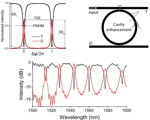
0 1 0.0
0.5 1.0
N
or
m
al
iz
ed
in
te
ns
ity
∆φ/2π T D
ERD
ERT
FWHM FSR
input T
D
Cavity enhancement
1500 1520 1540 1560 1580 1600
-15 -10 -5 0
In
te
ns
ity
(d
B)
Wavelength (nm)
Figure 1.9: Ring resonator example and spectral response.
to reduce the mode losses. The SOI platform with its tight waveguide geometries,
ensures such high confinement. Usually, ring resonators are coupled with a bus by
the co-directional evanescent coupling method. The transmission spectrum of the bus
waveguide with a single ring resonator will show dips around the ring resonances. This
way, the ring resonator behaves as a spectral filter, which can be used for applications in
optical communication, especially wavelength division multiplexing (WDM). There are
several types of resonators as, microdisks, polygonal microdisk, microspiral and double
notch-shaped microdisk [76] , but we are going to focus on the most used types in the
ONC, i.e. ring and racetrack resonators. Ring resonator is the most widespread single
mode cavity. The racetrack resonator is the answer to the needs of high coupling to
the bus waveguide in the case of a high confined mode. A microresonator coupled to 2
0
0
ADF
Add
Drop
In
Through
0
Figure 1.10: Schematic view of an add drop filter
bus waveguides is called add-drop filter (ADF). The wavelength selectivity of this device
makes it suitable to route a single wavelength to the through or drop port. While the
add port is used to add a new wavelength into the network. These features have brought
shape the system optical response for the final application, multiple resonators are used
both in coupled and in uncoupled configurations.
Applications include band filters [9], multi-bit delay lines [8,77], slow-wave devices [78]
and high-sensitivity sensor functionality [79]. The parameters of the individual ring
resonators and the coupling between ring resonators and input/output waveguides give
the degrees of freedom to be used in the design to tailor the device characteristics to
the required specication. The Vernier effect is often exploited to create filters with
an extended FSR [80]. The design of multi-ring resonator circuits in silicon requires
knowledge of effects with a particular influence in silicon: ring resonance matching,
process biases and coupling induced frequency shifting (CIFS) [81].
The resonance matching of ring resonators in a multi-ring device plays a critical role.
Even in tailored process technology, the uniformity of ring resonators closely packed (i.e.
placed in nearby position on the chip) is of the order of 0.5nm. This is of the same order
as the typical channel spacing used in a WDM system or of the resolution required for
sensor devices. In cascaded ring devices, this will lead to faulty devices if the rings are
not tuned or trimmed. However, trimming process requires extra power which decreases
the power efficiency of the network.
1540 1545 1550 1555 0.0
0.5 1.0
N
o
rm
a
liz
e
d
T
i
n
te
n
s
it
y
Wavelength (nm)
N=1 N=2 N=4 N=8
. . . .
CROW SCISSOR
Figure 1.11: Spectral response examples of CROW (image taken from [22]) and
SCISSOR.
The two common configurations of sequence of ring resonatros are the Coupled
Res-onator Optical Waveguide (CROW) and the Side-Coupled Integrated Spaced Sequence
Of Resonators (SCISSOR). The CROW configuration is being used to make the optical
analogue of electronic high order filtering and for optical delay line. The SCISSOR can
generate large flat stop band [82] and is being used to controll the device dispersion
and to slow down the light [83]. SCISSOR are also used for other applications, such
as: all optical analogous of the electromagnetic induce transparency [11], slow light [78],
tunable delay line [84,85] and XOR/XNOR logic [86].
As mentioned above, variation in device dimensions due to fabrication process variations
of devices. Since the process of tuning do not require a fast time response, thermal tuning
is the most widely used technique because of the large thermo-optic response of silicon
[4]. This is achieved by using micro-heaters. The most common heater conguration
is placing the heater on top of the device after a layer of silica to avoid the optical
mode coupling to the metal. The silica, being an insulator, has the advantage to limit
the thermal crosstalk to the nearby cavities but limits also the tuning efficiency. The
Figure 1.12: Heater example.
thermal efficiency can be improved by reducing the heat loss and confining the heat flow
to the device, which resulted in an efficiency of 4.8nm/mW but with a slow tuning speed
of 170µs[87] . A similar approach was followed in [88], where the silicon substrate was
removed to improve conduction loss.
Another method corrects the resonance position after the device production by a
mod-ification of the cladding refractive index either by using photo-oxidation of polymer
cladding [89] or by inducing stress to BOX layer [90]. This trimming method is
perma-nent and cannot be reversed.
1.1.3.1 Optical router
The thermo-optic switches integrated in a network topology constitute an on-chip optical
router. Here we give an example of a representative microresonator-based optical router.
Sherwood-Droz et al [91] demonstrated a 4×4 nonblocking silicon optical router using
thermo-optic switching. The device uses eight microring resonators and ten waveguide
crossings, with a footprint of 0.07mm2 [91]. The insertion loss of each crossing was
shown to be 0.51dB. Their design enabled bidirectional communications among the
four input ports and the four output ports. Each communication path demonstrated a
maximum extinction rate of 20.79dB and a bandwidth of 38.5GHz. The shortcomings
of such optical routers are relatively slow switch on/off times, of the order ofµslinked to
the used switching method, and a relatively high power consumption for the resonance
Cross grid
Banyan network
Microring resonator cross-grid array
(2000)
Third-order coupled microring
resonator cross-grid array
(2008)
Two microring resonator coupled
cross-grid array (2007)
4x4 optical hittless router (2008)
Second order coupled microdisk resonator
based add-drop filters array
Non-blocking
Non-blocking Third order coupled miroring for each cross-grid
4x4 switch Each crossing routes two links simultaneously Blocking
4x4 switch Non-blocking
4x4 switch
Multiple wavelength channel for routing Non-blocking
Figure 1.13: Some examples of router matrix topologies. [21]
1.1.3.2 Coherent control of the routing
Resonance lineshape tuning by means of coherent interference provides additional
func-tionalities. This means that the routing protocol is not only the wavelength, as for
a resonant system, but also the signal phase, as commonly used by Mach-Zehnder
in-terferometers. There are three common schemes proposed and demonstrated in silicon
microresonators:
1. coherent interference between a microresonator resonance and a detuned
microres-onator resonance, as in electromagnetically induced transparency (EIT) [11].
2. coherent interference between a microresonator resonance and a nonresonant
back-ground, as in Fano resonances [92]
3. coherent interference between a microresonator resonance and a coherent feedback
[93]
df
df
(1) (2)
(3)
Figure 1.14: Phase based routing devices: (1) CRIT , (2) Micro resonator with
feedback, (3) Mach-Zehnder assisted by a micro resonator. [22]
1. SCISSOR structure that exhibits the coupled resonator induced transparency
(CRIT) [33]. EIT-like phenomenon can occur in a microresonator system in
which two coupled microresonators coherently interfere [11]. The coherent signal
from two slightly detuned microresonators destructively interfere at the
through-put port. Such silicon coupled microresonator structures with EIT-like lineshapes
have found applications in tunable optical delay lines [84,85] or DWDM [34].
2. Resonance interference with a coherent feedback The resonance lineshape can also
be enhanced or suppressed by means of interference with a coherent feedback
[93]. By tuning the feedback phase and amplitude it is possible to enhance or
suppress the resonance. Such coherent feedback control highly depends on the
resonance wavelength thus, the resonance lineshape modulation varies among
res-onances. The feedback-microresonator, that enables controlled resonance lineshape
tuning with a large dynamic on-off ratio, offers more functionalities than simple
waveguide-coupled microresonator resonators. The fact that the phase and the
mi-croresonator resonance can be tuned separately it has been used for reconfigurable
filters [93,94], switches and modulators [76,95].
3. Resonance interference with a coherent background. The first proposed
config-uration was a MZI assisted by a microresonator [92]. The resonance pathway
corresponds to the lightwave propagating in the microresonator-coupled MZI arm,
and the coherent background pathway corresponds to the amplitude-split lightwave
propagating in the MZI reference arm. The two lightwaves recombine at the MZI
output ports. The system transfer function is characterized by an asymmetrical
phase in the MZI reference arm. The sharp asymmetrical lineshapes find
applica-tions in biosensing [96]. The MZI-coupled Micro resonator have also been proposed
for tailoring the filter lineshape with a flat-top and box-like spectral response [97].
1.1.4 Active modulators
Apart from the already discussed thermo-optic modulation, that is mainly used for
trim-ming, modulation in silicon is most commonly achieved by means of free carrier
disper-sion effect [4]. Free-carrier density changes induce changes in the refractive index which
modulates the light. Several different mechanisms for manipulating free-carrier densities
have been implemented in monolithic devices [98]. Among them, carrier-depletion mode
devices, usually based on a reverse-biased pn junction, are widely used to achieve high
speed. Since the first GHz silicon modulator was demonstrated by Intel [99],
modula-tor performance metrics have been significantly improved. Mach-Zehnder interferometer
(MZI) structures [100] are typically used for amplitude modulation. With traveling-wave
designs, data rates of up to 50Gb/shave been experimentally demonstrated [101,102].
At 20Gb/s, a record low power consumption of 200f J/b has recently been reported
[103]. Resonant structures can be used to dramatically reduce device footprints and
further reduce power consumptions, although at the cost of a significantly narrower
op-erating wavelength window and high thermal sensitivity. First introduced by Xu et al.
[10] in 2005, high-speed ring modulators have been demonstrated to operate at up to
40Gb/s [104] and, recently, were reported to achieve 7f J/b at 25Gb/s and with
ther-mal tuning capabilities [105]. Recent development includes breaking the cavity photon
lifetime limit by means of coupling modulation [106].
Si Si wg
p+ n
-SiO2
SiO2
n
-p+ doped
Vf
In
Out
Waveguide Ring
1.1.5 Delay lines
Optical delay lines are another key component for on-chip optical interconnects. The
traditional way to obtain optical delay is by passing the light through a dispersive
medium. Other than relying on a strongly dispersive medium, the strong dispersion can
be obtained from microresonator based structures. Figure1.16summarizes the
state-of-the-art of microresonator-based optical delay lines on silicon chips found literature. The
key performance metrics for the optical delay lines are time delay, bandwidth, insertion
loss and delay tunability. The figure-of-merit is the delay-bandwidth product (DBP).
Figure 1.16: Comparison between several delay line structures. [22]
1.1.6 Detectors
At the operating wavelengths of a silicon photonic chip, materials with a narrower
bandgap than silicon need to be integrated to function as the detection (absorption)
medium. Germanium or SiGe can be grown and can absorb light at the
telecommu-nication wavelengths [107], which is necessary for compatibility with standard CMOS
infrastructure. Bonded III-V materials are also used for photodetection [108], based
on bonding technologies. These materials are integrated close to or directly connected
to a silicon waveguide, so that the guided light can be evanescently coupled or butt
coupled into the photodetector and the photodetector can have a small cross section to
reduce device capacitance and improve speed [109]. The state of the art of germanium
photodetectors, in a photodiode configuration, is a 120GHz bandwidth with
wavelength of 1.550nm[110], which amounts to 84% quantum efficiency. Very low
pho-todetector capacitance of 2.4f F has been achieved in a photoconductive device [111] with
an estimated quantum efficiency of 90% operating with a bandwidth of 40GHz. Low
bias avalanche detection with 10dB gain and improved noise performance was achieved
by IBM, with a speed exceeding 30GHz [112].
1.1.7 External interface: grating coupler
One of the drawbacks of the high refractive index contrast is the large mismatch in
mode size and mode shape between the fundamental mode of the SOI waveguide and
the mode of the optical fiber, making efficient coupling of light from waveguide to fiber
an important issue.
Λ
1500 1550 1600
0.0 0.5 1.0
N
o
rm
a
liz
e
d
i
n
te
n
s
it
y
Wavelength (nm)
Figure 1.17: A grating coupler sketch together its spectral response.
In the literature, one-dimensional [113] and two-dimensional [114] grating structures
were proposed to tackle this problem. These grating couplers have the advantage to
enable wafer-scale testing of the integrated circuits and holds the promise of low-cost
packaging. Furthermore, they are very compact and have a large optical bandwidth.
Although one-dimensional structures are polarization dependent, a polarization diversity
scheme based on a two-dimensional grating coupler can be used in practical applications
[114]. To obtain a high coupling efficiency, different strategies can be followed. By
including a bottom mirror to redirect the downward diffracted light, a high coupling
efficiency can be obtained. This can be a metallic mirror [115] or a distributed Bragg
reflector-type mirror [116]. Another way to improve the coupling efficiency is to optimize
the design parameters of the grating unit cell while tailoring the pitch and duty cycle of
the individual grating periods [117]. The use of a slanted grating coupler was proposed
efficiency of these devices, which settles around 20% with relative ease, and the complete
compatibility with the CMOS process makes them the best candidates for interfacing to
the outside world an integrated photonics chip.
1.2
Non linear optics on chip
The high index contrast provided by SOI platform allows to have a tight light
confine-ment in a sub-micrometer waveguide. Such a small confineconfine-ment enhances the material
non linearities as a consequence of a higher power density. Moreover, the silicon
third-order nonlinearity exceeds that of silica exhibiting a Kerr coefficient 100 times larger
[120] and a Raman gain coefficient 1000 times larger [121] in the telecom window .
Sili-con is also optically transparent above 1.1µmallowing to realize low loss photonics device
[122]. Therefore, a great effort has been used to study nonlinear effects in silicon as
self-phase modulation (SPM) [123,124,125,126], cross-phase modulation (XPM) [127,128],
stimulated Raman scattering (SRS) [78,129], and four-wave mixing (FWM) [130,131].
Furthermore, the semiconductor propriety of silicon together with the imaginary part of
the third-order nonlinearity give rise to several peculiar effects as two photon absorption
(TPA) [120,123], free-carrier dispersion [4], and anisotropic and dispersive third-order
nonlinearity [132]. The passive and active linear and nonlinear proprieties of SOI based
photonic devices allow many degrees of freedom to create integrated optical devices for
practically whichever applications [133,134,135,136].
Naturally, in a microresonator these effects become more pronounced, since close to a
resonance there is a strong increase in power density. In magnitude, the thermal effects
are actually dominant, but they are slow. Bistable behavior has been demonstrated
in silicon microring resonators [43, 44]: the increased optical power will result in a
skewing of the resonance peak. This is illustrated qualitatively in Fig. 20 for the drop
port transmission of an ADF filter. At a certain power level, the resonance peak will
fold back, resulting in three possible transmission levels, of which only two are stable
solutions.
The thermal nonlinearities translate the optical power into a phase shift. A similar
effect occurs with the free carriers generated through TPA. The resulting free carriers
can be used in a ring resonator to induce a non-linear change in the real part of the
refractive index [42, 137]. These carrier effects are much faster than thermal effects.
When combining both effects with a different time scale, this can result in self-pulsing
1.549 1.550 1.551 1.552
0.00 0.05 0.10 0.15 0.20 0.25 0.30
Time (ns)
Self pulsing
Optical bistability
Figure 1.18: Optical bistability and self pulsing phenomena.
Together to the self pulsing effect, theoretically it was predicted the existence of chaotic
states in coupled cavity systems with a kerr nonlinearity [46,141,142]. This effect has
not yet been demonstrated experimentally. Chaotic system in integrated device could
Optical network on chip
components and its applications
2.1
Introduction
In the first part of this chapter, will be presented a brief introduction on the theory of
WGs and their applications. With the help of the COMSOL software the parameters
of the SOI WGs, that will be used during the rest of the work, will be estimated.
In particular, the coupling coefficients for a directional coupler (straight-straight and
straight-curve) and the effect of the surface roughness in a straight WG will be calculated.
The effect of a WG bend on the guided mode inside a WG will be also described by
simulations [143].
The second part of this chapter will introduce the optical microresonator component
with information about the main sources of linear losses, e.g. line edge roughness (LER)
induced losses. Theory will be developed by means of simulations performed using a
transfer matrix code. Examples will be given only for a racetrack resonator since it is
almost equivalent to a ring resonator with an elongated coupling section. The theoretical
transmission spectrum and the group delay are presented. Then, several test samples
are experimentally investigated in order to estimate the values of losses, of the effective
index, of the group index and of the effective curved index. The extracted parameters
are introduced in the transfer matrix code which is then used to design new devices and
to understand the experimental results.
We design the width of our waveguide for both TE and TM polarization while still
preserving the single mode condition. The racetrack resonator (RTR) and the ring
resonator (RR) are the resonators types treated. The former is used in the case of TE
polarization, where the high mode confinement does not ensure enough coupling to the
bus WG, while the latter is used in TM polarization since, the small effective coupling
section limits the coupling to the bus WG in the case of TE polarization. One of the
advantage of the use of silicon as guiding material is to allows using small bending radius
while maintaining low losses. Therefore, in our work we use bending radii of maximum
7µm in order to minimize the footprint of the final device.
2.2
SOI based Optical waveguides
All the waveguides (WG) used through this work are SOI based and are covered by a
SiO2 layer. That means that the index contrast between the core and the cladding is
symmetric in thexy plane (See Fig2.1). This has important consequences, as this type
of geometry allows always the propagation of the fundamental mode. Thus it is possible
to shrink the WG size maintaining the condition of guiding light.
Si SiO2 SiO2
Si
z y x
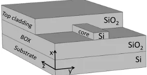
Figure 2.1: Example of SOI based optical WG. For clarity part of the top cladding has been removed to better show the core.
A sketch of a SOI WG is shown in figure 2.1. The guiding material is provided by the
silicon core with a refractive index of 3.4. The core hosts the most of the optical mode
power. The index contrast is provided by the silica box and top cladding that have
a refractive index of 1.4 . In this configuration the index contrast is 2.4, 2 orders of
magnitude greater than that of an optical fiber. In fact, the SOI material provide the
basis for the high index contrast photonics. A high contrast allows to fabricate devices
with a very small footprint. For example, a bend can be reduced up to the wavelength
of the traveling light while maintaining low losses.
Generally TE or TM linearly polarized light will be used. The definition of TE is shown
in Figure 2.2, where it is seen that the electric field exists only along the yz plane. The
TM is characterized by the electrical field in the xz plane since E and H are orthogonal.
The z axis indicates the propagation directions.
These support materials allow to build sub-nanometer guides maintaining low losses.
A guide with characteristic dimensions smaller than the wavelength of the guided light
z y
x E
H
Figure 2.2: TE polarized light. Z is the propagation direction.
is the heart of integrated photonics and is one of the foundations for the construction of
complex integrated photonic networks.
2.2.1 Waveguides theory
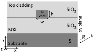
Figure2.3represents the cross section of a SOI based WG. A wave propagating through
the z direction in the core is guided or not depending on the value of the angleφicreated
by the wavevector k and xy plane. φi must be greater than the critical angle defined
as sin(φc) =ncl/nco wherencl and nco are the refractive index of the cladding and the
core respectively.
Si core
SiO2
SiO2
h w
Si
Top cladding
BOX
Substrate y
x z
i
φx
y
p
la
n
e
k
Figure 2.3: Left: Cross section of a WG and its characteristics dimensions: the height hand the width w. The z axis indicates the propagation direction and the xy plane contains the oscillating fields. Right:lateral view of the WG with the definition ofφi.
The electric(magnetic) field of an electromagnetic wave propagating through the z
di-rection in the core can be written as:
~
E=E0e
~
kz±ωtH~ =H
0e
~
kz±ωt (2.1)
The term φ=~kz±ωtis called phase of the field. The time variations of phase gives
∂φ
∂t =ω (2.2)
The spatial variations of phase gives
∂φ
∂z =k (2.3)
wherekis thewavevector of the wave. The propagation in the core material is described
by the refractive index:
k=k0nco (2.4)
wherek0 is the free space wavevector ant is related to the wavelength by
k0 =
2π
λ (2.5)
k
yk
xk
zi
φ
k
core
Figure 2.4: Wavevector decomposition inside the core.
The wavevectork can be decomposed into its components xyz,
~k=kxxˆ+kyyˆ+kzzˆ kz =k0ncosin(φi) (2.6)
valid for a k lying in the xz plane. The z component is imaginary and is also called
kz = β, the propagation constant of the wave. The z wavevector component depends
on the medium refractive index and on the incident angle. In the core of the WG, the
components kx and ky are imaginary while in the cladding these are real. This means
that the field will be attenuated exponentially to a degree determined by the decay
constant following this law:
Excl(y)=E0cle−kx(y)x(y) (2.7)
Excl(y) represents the field amplitude in the cladding. The fact that the field outside
the core is non-zero is represented by the evanescent field concept. It is worth to say
that, evenβ in a real case has a real part, calledα, which is related to the losses of the
For the x axis, for example, we can write the phase shift (neglecting the delay at the
boundaries) as:
φw = 2kxw= 2πm (2.8)
where m is the mode number that comes from the discretization of the eigensolutions,
called modes, along this axis imposed by w, the width of the WG (see fig. 2.3) . Such
a treatment may also be made for the ky, considering h the height of the core. The
confinement along y adds another mode number, n. The mode identified by m = 0
and n = 0 is called the fundamental mode. Therefore, the WG dimensions, the index
contrast (or the incident angle equivalently), the light wavelength and the polarization
set the number of allowed modes in the WG. Depending on these parameters may exist
single mode or multi mode WG. Figure 2.5shows the field distributions of these modes
labelled by the termT EMmn.
Figure 2.5: Rectangular transverse mode patterns T EMmn. Image taken from
Wikipedia.
The mode numbers are the evidence of the fact that there are two standing waves that
propagate in the x, y direction. These values correspond to the number of minima
of the field profile along x, for m, and along y, for n. β is an important parameter
because describes the rate at which a wave propagates. To simplify the treatment of
the propagation of light, the effects of the incident angle may be incorporated inside the
effective index, nef f. Fork lying in the xz plane, we define it such that:
nxzef f =ncosinφi
Then the equation for β becomes:
Note the similarity with the equationk=k0nco. This is equivalent to think of the mode
as propagating straight down the waveguide, without bouncing back and forth, with an
effective refractive index nxzef f. The effective indexnef f is then calculated making the
same considerations but for theyzplane and by using, instead ofnco,nxzef f. The effective
index always ranges between the core index and the cladding index.
To describe the magnitude of the evanescent field, the field which propagates out from
the core, it is usually used the confinement factor. This parameter is the ratio between
the energy confined in the core and the sum of the energy in the core and in the cladding.
It is defined as [144]:
Γ =
R R
coreE2(x, y)dxdy
R R∞
−∞E2(x, y)dxdy
(2.9)
2.2.2 Simulations of waveguides
The WG is the basis of any integrated ONC. In this section we want clarify the order
of magnitude of the fundamental parameters that characterize a WG, in order to have
the basic guidelines to develop the structures studied throughout this work.
SiO2
SiO2
h
w
Si nco
ncl
htop
hBOX
Figure 2.6: Cross section of a WG and its characteristic dimensions, the heighth, the width w. hbox is the height of the buried oxide layer andhtop is the height of the
top cladding.
Figure 2.6 shows the section of the used waveguides. They are of the strip WG type.
The constructive parameters are given in the following table:
Table 2.1: WGs parameters
h w hBOX htop nco ncl
TM 220nm 500nm 1.5−2µm =0.75µm 3.47 1.44
TE 220nm 450nm 1.5−2µm =0.75µm 3.47 1.44
As can be seen, it was chosen a different width for the two polarizations in order to allow,
for both, only the propagation of the fundamental mode at the wavelength of 1550nm
and avoid the coupling between the TE and TM mode (i.e. birifrangence). The refractive
function of the wavelength through the Sellmeier equations in order to compensate for
the material dispersion. In the table we specified these values forλ= 1.55µm. In what
follows, if it is said that a device is designed for the TE(TM) polarization, then the WGs
of which it is composed have a width of 450nm(500nm).
Here is reported a table with the commonly used values of the BOX and of the WG
height found in the literature:
Table 2.2: SOI wafer thickness specification for silicon photonics found in literature
WG height (nm) BOX (nm)
IBM 220 2000
MIT 220 1000
Uni. Glasgov 260 1000
Cornell Univ 240 3000
Intel 500 1000
From figure2.7it is possible to see that the TM mode has substrate losses 1 or 2 order of
magnitude higher than the TE mode. This is due to the less vertical confinement of TM
mode. In this work we use a BOX of 1.5µmthat gives losses of about 0.1dB/cm. In any
case, in order to estimate the losses of a mode, the scattering losses due to roughness
have to be taken into account since they typically dominates(see section2.6).
0 . 8 1 . 0 1 . 2 1 . 4 1 . 6
1 0 - 4 1 0 - 3
1 0 - 2 1 0 - 1
1 0 0
1 0 1
L
e
a
k
a
g
e
l
o
s
s
(
d
B
/c
m
)
B O X t h i c k n e s s (µm )
T M T E
Figure 2.7: Substrate leakage loss in dB/cm as a function of BOX thickness (µm) for
the TE and TM polarization atλ= 1550nm
Figure 2.8 reports the simulated values of the effective index and of the confinement
factor (Equation2.9) for a wavelength range of 1500−1600nmand TE/TM polarization
of the fundamental modeT EM00.
We can see that the TM mode has a lower effective index compared to the TE mode.
The same applies to the CF. This is due to the fact that h < w. It is important to
remark that the CF for the TE mode is about 0.5. This means that half of the energy
1 5 0 0 1 5 3 0 1 5 6 0 1 5 9 0 1 . 7
1 . 8 1 . 9 2 . 0 2 . 1 2 . 2 2 . 3 2 . 4
1 5 0 0 1 5 3 0 1 5 6 0 1 5 9 0 0 . 1 0 . 2 0 . 3 0 . 4 0 . 5 0 . 6 ( b )
E
ff
e
c
ti
v
e
i
n
d
e
x
W a v e l e n g t h ( n m )
T E T M
( a )
C
o
n
fi
n
e
m
e
n
t
fa
c
to
r
W a v e l e n g t h ( n m )
Figure 2.8: (a) Simulated effective index for TE and TM polarization. (b) Simulated
confinement factor index for TE and TM polarization. Fundamental mode T EM00.
Simulation parameters reported in the tab2.1.
For convenience, the values of thenef f and CF are reported in table2.3
Table 2.3: nef f andCF for several values ofλand for TE and TM polarization
TE TM TE TM
λ(nm) nef f nef f CF CF
1500 2.417 1.840 0.62 0.21791
1525 2.386 1.800 0.611 0.20
1550 2.355 1.772 0.59 0.18
1575 2.324 1.741 0.58 0.16
1600 2.293 1.712 0.56 0.15
Observing the field profile of the WG in the picture2.9you can realize how much energy
travels outside the core. This has a negative impact on mode losses. A low confined
mode ”feels” more the presence of defects and roughness on the surface of the WG and
cladding, increasing its propagation losses.
TE
TM
Figure 2.9: Simulated fundamental mode profile for TE and TM polarizations. Plot of the Electric field module.
Just to give an idea, the modern CMOS facilities are able to produce sub-nanometer
treatment to reduce the surface roughness [146,147]. In fact, achieving low loss without
post processing is desirable to avoid fabrication overhead and complexities.
Some values of WG losses, found in the literature, are reported in the following table:
Table 2.4: WGs propagation loss comparison. Fabrication technology: 193 and 248nm
lithography. TE polarization.
Reference Cross-section(nm) TE loss (dB/cm)
CEA-LETI 512x200 4.18±0.21 [47]
MIT-BAE 420x200 8.2±0.5 [148]
470x200 5.7±0.5
520x200 4.6±0.5
570x200 4.3±0.5
Ghent Univ.-imec 515x220 2.74±0.06 [146]
500x220 2.73±0.1
485x220 2.85±0.07
2.3
Directional coupler
In the previous section we said that part of the field propagates outside the waveguide.
Let’s see how this effect is used in thedirectional coupler. These devices serve to exchange
energy between two WGs separated in space and are widely used in ONC.
The coupled mode theory (CMT) is the most fundamental theoretical approach to the
design and construction of practical integrated photonic devices.
CMT is the theory that describes the interaction between modes and the new modes
arising from the modified structure.
The fundamental principle on which it is based is that there is an orthogonal
rela-tion between the modes supported by a waveguide structure, which implies that each
mode propagates independently along the waveguide without power exchange among
the modes itself. The modes become mutually coupled when energy transfer between
them takes place if the original waveguide structure is altered.
There are many articles (see for example [149]) that describe in depth the CMT for
electromagnetic fields, here an approximate version is presented, anyway useful to
un-derstand the physics behind this phenomenon.
z y
x h
w
gap
1 2
Figure 2.10: System under study. w and h are the size of the WG, cg is the separation
between WGs (coupling gap). The two WGs are labelled whit 1 and 2 .
Let’s start from these equations
da1(z)
dz = i kca2(z)e
−(β2−β1)z (2.10)
da2(z)
dz = i kca1(z)e
(β2−β1)z (2.11)
derived from Maxwell’s equations in perturbation theory [150, 151]. These equations
describe the propagation of the fields a1 and a2 in the two WGs along the z direction.
kc is a field integral of the field which indicates how much of the two modes overlaps.
This parameter is strongly linked to the size of the evanescent field, that iskx,y. In the
CMT the approximation of kc small is used , i.e. kx,ygap >1, this means a rapid decay
of the field outside the WG.
F = 1
1−δ/kc
; δ =β2−β1
whereF is the power-coupling efficiency,β1and β2 are the propagation constants of the
first and second WG and 2δ is the mismatching. For two equal WGs β1 = β2. This
is called perfect phase matching conditions for which all the power can be exchanged
between the WGs, and F, the efficiency, is 1.
Using these ansatz
a1(z) = x1eikcz+x2e−ikcz (2.12)
a2(z) = y1eikcz+y2e−ikcz (2.13)
and solving for x1,2, y1,2 we obtain:
a1(z) = a1(0) cos(kcz)−a2(0)i sin(kcz) (2.14)
By imposing as initial conditions that only the first WG is exciteda1(0) =a0, a2(0) = 0,
we get:
a1(z) = a0 cos(kcz) (2.16)
a2(z) = −i a0 sin(kcz) (2.17)
To obtain the power exchanged between the WGs, we have to square them:
P1(z) = 1−sin2(kcz) (2.18)
P2(z) = sin2(kcz) (2.19)
with a0 = 1. These equations tell us that energy is periodically exchanged between
the WGs, with a period of kc. The maximum power coupled between the two WGs is
reached at z= 2πk
c(2m+ 1),(m= 0,1,2...) and the length z at m = 0 is called coupling
length (Lcp).
Lcp=
π
2kc
(2.20)
Even if the CMT works in a weak coupling regime, it can nevertheless be used to provide
an approximate representation of the light propagation in two strongly coupled photonic
WGs ( as, for example, working near Lcp).
To do that, we have to consider the two interacting WGs as one system where a splitting
of the first symmetric and second anti-symmetric order modes occurs. The equation for
the electric field can be approximated by a sum of the even and odd modes:
E(x, z) =Ee(x)e−i βez+Eo(x)e−i βoz (2.21)
with Ee,o and βe,o the even and odd mode electric fields and propagation constant
respectively. We can extract the coupling coefficient kc by looking at the eigen modes
of the previous equations. Forz= 0 we find the first eigen modeE1(x):
E(x, z) =|Ee(x) +Eo(x)|=E1(x) (2.22)
For anyz:
that atz= (β π
e−βo) becomes
E(x, z) =|Ee(x)−Eo(x)|=E2(x) (2.24)
whereE2(x) denotes the eigen mode of the second WG. If we compute at which length
there is the maximum power transfer we found:
Lcp=
π βe−βo
= π
2kc
, (2.25)
so finally the coupling coefficient is:
kc=
βe−βo
2 (2.26)
Using the relationβ = 2π/λnef f we can writekc as a function ofnef f.
kc=
λ
2 (ne
ef f)−noef f
(2.27)
Figure2.11is the cross section of the geometry in figure2.10. It shows the profile of the
Ex field within the structure for the TE polarization. The panel (a) shows the profile of
the even eigenstate while panel (b) the odd.
+
-Ex
Odd
Even
x
Figure 2.11: X component of the electric field for the even (a) and odd (b) modes.
Table 2.5: Relative effective index variations for the even and off mode
∆neef f ∆noef f nef f
160 nm −0.81% 1.1% 2.36
200 nm −0.62% 0.74% 2.36
The two eigenstates are characterized by an effective index which differs from that of the
single isolated WG: greater for the even and lower for the odd. The deviation fromnef f
is negligible for large separations but, in resonator systems where also a slight variation of
for small gaps. These are calledcoupling-induced resonance frequency shifts (CIFS) and
can have deleterious effects on high-order resonant filters [152]. For example, the relative
variation for aλ= 1550µm, a gap of 160nm and 200nm and TE polarization are:
∆neef f = 0.90%
∆n0ef f =−0.71%
The gap clearly influences the magnitude of the index mismatch.
The table below reports the values of Lcp for several parameters. The simulation refers
to the geometries defined in table 2.1.
Table 2.6: Lcpfor several values of gap
TE TM
λ(nm)\gap(nm) 160 180 200
![Figure 1.2: 3D integration of electronics and photonics on a single CMOS chip. Imagetaken from [16].](https://thumb-us.123doks.com/thumbv2/123dok_us/553817.2054887/10.596.175.456.81.292/figure-integration-electronics-photonics-single-cmos-chip-imagetaken.webp)
![Figure 1.4: Sketch of the WDM principle with zooms on the basic block: (a) Mi-croresonator based mux/demux, (b) AWG based mux/demux [24].](https://thumb-us.123doks.com/thumbv2/123dok_us/553817.2054887/12.596.147.487.357.563/figure-sketch-principle-croresonator-based-demux-based-demux.webp)
![Figure 1.13: Some examples of router matrix topologies. [21]](https://thumb-us.123doks.com/thumbv2/123dok_us/553817.2054887/23.596.163.472.82.408/figure-some-examples-of-router-matrix-topologies.webp)
![Figure 1.16: Comparison between several delay line structures. [22]](https://thumb-us.123doks.com/thumbv2/123dok_us/553817.2054887/26.596.148.491.253.462/figure-comparison-delay-line-structures.webp)