Page 263 www.ijiras.com | Email: [email protected]
Advanced PV System For Domestic Applications
Jeevan N D
Assistant Professor, Department of Electrical and Electronics Engineering, K.V.G. College of Engineering, Sullia, India
I. INTRODUCTION
Energy turns into the essential part of human lifestyle. The substantial boom within the electricity condition and the fast depletion of fossil fuels within the globe drives mankind towards the use of nonconventional electricity assets together with wind, solar, geothermal, etc. Amongst all non-traditional electricity assets solar electricity is suiting up since of this one recyclable, renewable and non-polluting nature. It has the brought benefits of sustaining no gas cost, fixed and sound less operation and subsequently much a smaller amount renovation requirements. It attracted the interest of the government, industries and researchers because of its zero greenhouse emission at some stage in its operation. The lifestyles cycle of the PV panel could be around two decades. Solar panels from the very best widespread production agencies may want to change 23% of the solar strength into electricity and it decreases to 10-16% at low sun radiation situations.
The electrical strength era in means of the PV board relies upon on the factors which include climate situations, sun emission level, ambience temperature, kind of PV cell and
arrangement quality. The energy switch since PV array to AC load is performed with energy specifies structures. For the reason that performance of the PV panel is poor, the electricity preparing device should have high efficiency[2]. The energy preparing system includes alteration stages. A dc-dc converter with most strength factor monitoring constitutes the primary degree and a dc-ac inverter providing electricity to the load is the second level[1]. The electricity production of the PV system may be expanded also via growing the solar irradiation the usage of solar trackers or by MPPT methods. The MPPT tracks the supreme electricity point of the PV arrangement under all special conditions and allocations as much as 96% of the most energy era of the PV array to the subsequent level. Execution of the MPPT strategies will increase the end product energy from solar array via 46.3% for a distinct fair weather day. This will be accomplished by the utilization of superior power electronics devices and the implementation of tender switching converter topologies. In dc-dc conversion stages its miles important to step up the voltage for most of the application. For this boost converter is the most appropriate preference. However to gain excessive voltage, the duty period of the converter ought to be more than zero and 95% is
Abstract: Conventional source like fossil fuel were used earlier to satisfy the energy demand. Nowadays these are being replaced by renewable source like photo-voltaic source. Photo-voltaic is a method of generating electrical energy by converting the energy from the sun into DC sources with the utilization of semiconductors device that exhibits photovoltaic effects. They do not cause environmental pollutions and do not requires any moving part. Different types of DC-DC Converter have been proposed in literatures but Inter-leaved boost Converters (IBC) is widely used because of its fast dynamic response and high power density. This paper presents analog design, and implementation of An Effective High Step ups IBC (Interleaved Boost Converter) Photovoltaic Grid Connection System. MPPT algorithm is incorporated into the developed controllers of the interleaved dc-dc converter to maximize the obtained power from the PV system. The interleaved dc-dc converters are compared with the normal boost converters topology. The interleaved dc-dc converter reduce a filter size due to the reduction in the ripple contents at the input and the output terminal of the converter. Designing of a closed loop controlled single phases inverters with SPWM is implemented for AC stand-alone load.
Page 264 www.ijiras.com | Email: [email protected] difficult to gain due to operational constraints. The interleaved
boost converter (IBC) brings down the conduction loss by the distribution of the input current and in turn will increase the performance. IBC has low current stress, decreased passive component size, small input current ripple and output voltage ripple.
A. LITERATURE SURVEY
Several investigations were carried out on the performance of Interleaved DC-DC converters. A brief review of the literature regarding this project is discussed in this section. There is a growing hobby in separate generating structures primarily established on extended electricity, anywhere the assembly towards the application is also difficult or high priced [4]. Minor separate PV structures offer electric power to lighting, indicators, water-pumps, and plenty of different minor power application [5]-[6]. They contain a MPPT to maximize strength output of the PV structures. Several MPPT techniques take to be established and differ in difficulty, sensors essential, union speed, price, and variety of usefulness, employment hardware, reputation and dissimilar aspects [7]. Interleaved converter switching on the equal frequency are worked during equivalent although by even phase modification among them [8]-[9]. This reasons an growth within the ripple frequency and a bargain in the ripple at the input and the output terminals of the converter [10]. These bring a compact filter size as compared to at least individual necessary for a solo converter without interleaving [11].
B. OBJECTIVE OF THE PROPOSED WORK
There is high need of solar energy utilization in house hold and the MPPT tracking is important of the design of PV based scheme. The Interleaved converters are used to solve the problem of current ripples in the boost converter. Main objective of the proposed paper is to design and simulate interleaved boost converter with MPPT for single phase home appliances.
II. PROPOSED STRUCTURE OF PV SCHEME FOR DOMESTIC APPLICATIONS
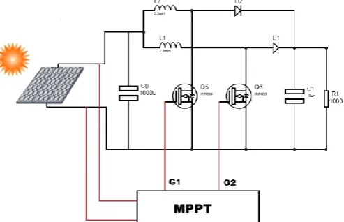
Figure 1: PV system for domestic applications
The above Fig.1 shows the proposed model of the PV scheme for driving domestic appliances. The solar panels are connected to interleaved step-up converter to step-up the voltage. The MPPT is utilised to track the supreme power drawn from the PV arrays. The controlled step-up output is given to the 1ϕ inverter is connected to the load. The controller produces pulses and the driver circuit is used to enhance the pulses and isolate from the MOSFET switches. A. PV MODULE AND MPPT METHOD
The two familiar versions for solar cell: single diode version and multiple diode version. Although multiple diode model is more accurate, its disadvantages outweigh the advantages it is because, the number of variable which should be calculated is more than one-diode model. Hence, for simulation in this project one-diode version is used[4].
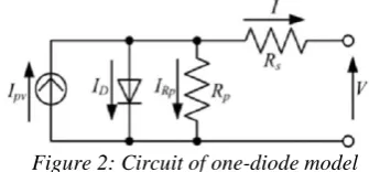
Figure 2: Circuit of one-diode model
PV cell contains one diode parallel with photocurrent sources. To have more accurate model series resistance and parallel resistance added to this combination. Fig 2 shows corresponding circuit of single diode model.
According to equivalent circuit output current of one PV cell is calculated as follows:
I=Ipv-ID-IRP ……….. (1)
I=Ipv-Io( -1) - ………….. (2)
Where IPV is the current producing by light radiation, I is
reverse capacity current, α is diode idealist factor. Vt which stands thermal voltage of PV module can be computed from equation below:
Vt = ………. (3)
Current producing through each cell is something among 2A to 10A and output voltage is lesser than 1V and depends on its material, for silicon is approximately 0.6V. Usually the cells are arranged to sort the output voltage increment of 12 V. Therefore, the output voltages of PV panels which are available in marketplace are 12V, 24V or 36V.
The same equation is utilized to model PV element, the only distinction is around output voltage and current, within the situation of voltage the whole output voltage would be divided by using the quantity of sequence cell and current is produced by using the amount of parallel sequence multiply by current respectively.
a. INCREMENTAL CONDUCTANCE METHOD
Page 265 www.ijiras.com | Email: [email protected] established on the differentiation of power w.r.t voltage, due
to this fact that this value in maximum power point is equal to zero.
= +Vpv =0………(4)
………(5)
Besides, is called instantaneous conductance and is incremental conductance, the place where these two values are equal the MPP will be there.
Figure 3: P-V arc module
Thus, meeting the MPP requires checking the operating point in each sample; generally operating points in a P-V curve are classified into three groups:
, Vpv<VMPP……….(6)
, Vpv=VMPP………...……(7)
, Vpv>VMPP………...…..(8)
Besides, the incremental variations can be stated approximately due to subtracting of actual value of VPV and
IPV in two following sampling time.
dIpv ≈ ΔIPV= IPV(t1)-IPV(t2)…………(9)
dVpv ≈ ΔIPV= VPV(t1)-VPV(t2)………(10)
Analysis of data values is much easier with this approximation. Algorithm flow chart of Inc.Cond method has been drawn in Fig. 4. Practically, it is impossible to achieve exact MPP ( 0), Consequently, more experimenting format is:
……….(11)
Figure 4: Algorithm flow chart of Incremental Conductance method
B. DC-DC CONVERTERS
DC-DC step up converter with MPPT controller have been utilized at the output of the solar array to offer power to the load. Step up converters are utilized PV energy packages due to the simple topology, rapid transient response then nonstop input current. Aimed at presenting excessive output voltage dc-dc converters needs to be worked at exciting inductors duty cycle, which would topics switching devices to small pulse which leads in reverse recovery and Electromagnetic interference troubles. Converters with attached can offer excessive output voltage then much a smaller amount of switching voltage stress exclusive of extreme duty cycle. However the trickle energy loss in the coupled inductor decreases the efficiency of the converter. C. OPERATION PRINCIPLE OF INTERLEAVED BOOST
CONVERTER
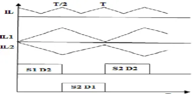
To enhance the overall presentation of the step-up converter adding method can be used. Interleaving is the process of connecting or extra switching converters in parallel as illustrated in Fig 5. In interleaved step up converters the i/p current ripple is decreased due to the summation of the inductor modern current through the L1 and L2 to get the
current iL as in figure 5. Because of interleaving the number of
inductors required decreases without altering its performance compared to normal boost converter[12]. The growth of no. of phases reduces the ripple content by an aspect of 9% in a dual phase interleaved converter in comparison to normal boost converter. However increasing the ranges of phases lacking restrict will rise the quantity of modules besides later the device price without huge fall in ripple. In entirely phases the range, form and ratings of the additives must remain the similar. The phase modification among the PWM controls indications carried out for exceptional stages must be 360/n wherein n is the no. of phases. For a 2-ϕ converter should be 180 degrees.
Page 266 www.ijiras.com | Email: [email protected] Figure 6: Wave forms of inductor current and switching
pulses
D. PROPOSE TECHNIQUES OF IBC
The technique at all types of IBC want a choice of appropriate value of inductors, capacitors & desire of the power semiconductors components to decrease the switching harms. The step tangled in scheming IBCs are as follow:
a. CHOICE OF DUTY RATIO AND QUANTITY OF
PHASE
Dual phase IBCs is selected because the ripples contented material decreases with growth in the no. of phases. Uncertainty the range of the phases is improved and much reduction in the ripple contents. Therefore, as a trade-off among the ripple contents material, cost & difficulty no. of phase is selected. The no. of inductor, switch and diode are identical as the no. of phase and switching frequency is same to all of the phase.
(0.31<D<0.67) …….(12)
b. CHOICE OF INDUCTOR
The choice of the appropriate inductors and capacitors the scheme equations part for the converter is:
Coupled Inductors
The equivalent inductances (Leq) for coupled IBC is
L = ……….. (13)
Where Vin signifies input voltage, D signifies duty ratio. The phases current ripple given as
ΔIphase= ………. (14)
To discover out the values of (Lm), the input current is designed by the input voltage and power. Through a coupling coefficient α of 0.61.
L= ……… (15)
Lm is considered as
Lm= αL……… (16) Input current ripple as
ΔIin= ………. (17)
Since the above calculations it is clear that growing the rate of the coupling factor can efficiently decrease input current ripple, then the phases currents ripples is amplified.
Consequently, the rate of couplings factor is sensibly selected as 0.61.
c. CHOICE OF POWER DEVICE
The semiconductors devices selected for building the 2ϕ interleaved boost converters is the MOSFET. The principle profit of MOSFET is lesser on states resistances, lesser transmission loss and greater switching action. The highest voltages throughout the switching device is set as
Vswitch=Vin ………..(18)
The diode has much a smaller amount forward voltage, maximum reverse breakdown voltage and much low reverse recoverie current which ends up in decreased switching losses. Appropriate to lack of reverse recovery current, and no requires of active snubber circuits for safety. Therefore the circuit difficulty is minimized. Circuit dependability is stepped forward and designed of the converters is easy.
d. FILTERS
Capacitors filters are essential at the outputs to restrict the ripples of the output voltages. The capacitance of the output filter are purpose of the duty cycle, frequency and smallest load resistance for the duration of full load. Designed for 6% output voltage ripple, the rate of the capacitance is specified assumed by,
C= ………. (19)
Where R defined as load resistance, Vo defined as output voltage and T defined as switching period.
III. SIMULINK MODEL OF CLOSED LOOP CONTROL OF PROPOSED SYSTEM
Designed values used for closed loop system are: Input Voltage (Vin) = 120V
Input Inductor (L1 & L2) = 6.3130×10⁻⁵ H C1 = C2= 100μF
R =50Ω
Page 267 www.ijiras.com | Email: [email protected] Figure 8: Simulink model of pulse generator for proposed
converter
Figure 9: Simulink model of MPPT controller
IV. SIMULATION RESULTS OF PROPOSED SCHEME A. PHOTO VOLTAIC OUTPUT
Figure 10: Photo voltaic output voltage
Fig. 10 shows the Photo Voltaic output voltage & current with the function of time, the output voltage is 120V & output current is 16A.
B. GATE PULSES FOR THE MOSFETS
Figure 11: PWM output
The gate pulses for the MOSFETs are shifted by 360/n for an „n‟ phase design. Since the no. of phases selected here is 2, the pulses be shift by 360/2 i.e., 180 degrees apart.
C. INTERLEAVED BOOST CONVERTER OUTPUT
Figure 12: Interleaved Boost Converter Output
Fig.12 shows the interleaved boost converter output of voltage by the characteristics of time; the output voltage is 240V.
D. THD VALUE OF SINGLE PHASE INVERTER
Figure 13: THD value of single phase inverter exclusive of 2nd order filter
Fig.13 shows THD value of 1.63% of Single phase inverter output voltage without second order filter connection. E. SINGLE PHASE INVERTER OUTPUT
Figure 14: Single phases Inverters Output
Fig. 14 shows the single phase inverter output of voltage by the characteristics of time, the output voltage is 240V. F. SUMMARY OF SIMULATION RESULT
Photo voltaic output 120V Interleaved step-up converter output 240V DC
Single phase inverter output 240V AC
Ripple current 0.03A
Voltage ripple 0.00028V
Table 1
V. CONCLUSION
Page 268 www.ijiras.com | Email: [email protected] MPPT. A contrast among the conventional and IBC converter
is offered to reveal up the result of interleaving. The use of interleaving in boost converter reasons an amplify in the ripple frequency as well as decrease in the ripple contents at the input and the output terminal of the converters which grades into a reduced filter size. Ripple cancellation exist a characteristic of the duty cycle of a converter and number of phases.
REFERENCES
[1] D.Meneses, F.Blaabjerg, O.Gracia, and J.Cobos, "Review and Comparison of Step-up Transformer less Topologies for Photovoltaic AC-Module Application", IEEE Transactions on Power Electronics, Vol.28, No.6, pp.2649-2663, June 2013.
[2] B. Alajmi, K.Ahmed, G.Philip, and B.Williams, "Single-Phase Single Stage Transformer less Grid-Connected PV System", IEEE Transactions on Power Electronics, Vol.28, No.6, pp.2665-267, June 2013.
[3] G. Velasco-Quesada, and F.Guinjoan-Gispert, R. Pique-Lopezand, M. Roman-Lumbrers, and A. Conesa-Rosa, “Electrical PV Array Reconfiguration Strategy for Energy Extraction Improvement in Grid connected PV Systems” IEEE Trans. on Industrial Electronics, 2009.
[4] Eduard Muljadi, “PV Water Pumping with a Peak-Power Tracker Using a Simple Six Step Square-Wave Inverter”, IEEE Transactions on industry applications, Vol.33, No.3 May/June 1997.
[5] S. Mekhilef, N. A. Rahim, and A. M. Omer, “A new solar energy conversion scheme implemented using grid-tied
single phase inverter”, Proceedings of IEEE TENCON-2000, Kuala Lumpur, Malaysia, 2000.
[6] VarinVongmanee, “The photovoltaic pumping system using a variable speed single phase induction motor drive controlled by field oriented principle”, The 2004 IEEE Asia-Pacific Conference on Circuits and Systems, December 6-9, 2004.
[7] Mona N. Eskander and Aziza M. Zaki, “A Maximum efficiency photovoltaic-induction motor pumping system”, Renewable Energy, Vol. 10, No. l, pp. 53- 60, 1997.
[8] Jancarle. L. Santos. Fernando Antunes. AnisChehab. C‟cero Cruz, “A maximum power point tracker for PV systems using a high performance boost converter”, Solar Energy 80 PP 772–778, 2006.
[9] D. Nguyen, and B.Lehman, “An Adaptive Solar Photovoltaic Array using Model-based Reconfiguration Algorithm ” IEEE Trans. on Industrial Electronics, 2008. [10]P. W. Lee, Y. S. Lee, D. K. Cheng, X. C. Liu,“Steady-state analysis of an interleaved boost converter with coupled inductors,” IEEE Trans. Ind. Electron., Vol. 47, Issue 4, pp. 787-795, Aug., 2000.
[11]Y.Kim, Y.Ji, J.Kim. Y.Jung, and C.Won, „„A New Control Strategy for Improving Weighted Efficiency in Photovoltaic AC Module-Type Interleaved Fly back Inverters‟‟, IEEE Transactions on Power Electronics, Vol.28, No.6, pp.2688-2663, June 2013. Electronics, Vol.28, No.6, pp.2688-2663, June 2013.