Vol. 2(10), 2010, 5526-5533
FPGA BASED DESIGN &
IMPLEMENTATION OF SERIAL DATA
TRANSMISSION CONTROLLER
A.R.M. KHAN
Department of Electronics & Telecomm, Jawaharlal Darda Institute of Engineering & Technology Yavatmal Maharashtra-445001, India
A.P.THAKARE
Member IEEE, Head of Department of Electronics & Telecomm, Sipna’s College of Engineering & Technology, Amravati. Maharashtra-444606, India
Abstract:
In most of the applications, the physical systems require a real-time operation to interface high speed constraints. This paper presents an experimental design and implementation of the I2C bus controller as per the specification
given by the Philips, on cyclone-II EP2C35F72C6 FPGA in Altera DE2 board.I2C bus controller was designed using
VHDL language, which demonstrates the complete I2C protocol operation to drive the Wolfson Codec WM8731,
where Altera Quartus II 9.0 is used for the synthesis and ModelSim- Altera 6.5b is used for the simulation. Using the I2C bus as a communication channel, the master controller will be able to send data to the slave and the slave
will response accordingly. Utilization of FSM reduces the synthesized hardware. Designed controller is mapped to FPGA of 90nm technology, out of 33,216 LEs, 55 LEs are used in the design and 8 I/O pins are used from 475 pins of FPGA.
Keywords: I2C bus controller; Wolfson Codec; cyclone-II FPGA; Quartus II; ModelSim.
1. Introduction
The physical size of ICs has reduced dramatically over the years. The main reason, of course, is attributed to the fact that more and more transistors can be cramped into a smaller space. A less mentioned reason is because the pins for interconnections between ICs have also decreased both in size and in number. As you probably know, the actual circuitry of the IC is much smaller than the packaging of the IC. The reason why the packaging has to be larger is because of the larger pins needed for the connections on the PCB by using the Inter-Integrated Circuit bus the number of pins requirement get reduced[Enoch (2008)]. USB/SPI/MicroWire and mostly UARTS are all just 'one point to one point' data transfer bus systems. USB then uses multiplexing of the data path and forwarding of messages to service multiple devices. Only CAN and I2C use SOFTWARE addressing, to determine the participants
in a transfer of data between two (I2C) or more (CAN) chips all connected to the same bus wires. I2C is the best bus
Table.1 Pros & Cons of Serial Buses Available
BUS PROS CONS
UART Well Known
Cost effective, Simple
Limited functionality
Point to Point
CAN Secure, Fast Complex,
Automotive oriented
Limited portfolio, Expensive firmware
USB Fast
Plug & Play HW
Simple
Low cost
Powerful master required
No Plug & Play SW –Specific drivers required
SPI Fast
Universally accepted
Low cost
Large Portfolio
No Plug& Play HW
No“fixed” standard
I2C Simple, Well
known
Universally y accepted
Plug &Play
Large portfolio Cost effective
Limited speed
2. DE2 Development Board
Vol. 2(10), 2010, 5526-5533
Fig. 1 Block Diagram of DE2 Board [Altera (2006)]
3. Structure of Serial Transmission Controller
The controller is design and implemented for the transfer of the data from FPGA to the Wolfson codec with the two line I2C (Inter-Integrated Circuit) protocol , the FPGA communicates with the Wolfson codec using two pins:
'SDIN' (the data line), and 'SCLK' (the bus clock) . The figure (2) shows the actual system used in the implementation of the I2C protocol. Design use the LED from the DE2 board to verify the operation after
implementation of the protocol, the reset and the word enable, control the data transfer on the SDIN line of the protocol.
Fig. 2 Block Diagram of control System
3.1 I2C Protocol Specification
The I2C bus is a very easy bus to understand and use. I2C is the best bus for low speed maintenance and control
applications. Where rise time is measured between 30% and 70% of VDD. This becomes important when buffers ‘distort’ the rising edges on the bus. By keeping any waveform distortions below 30% of VDD, that portion of the rising edge will not be counted as part of the formal rise time.I2C is a low to medium speed serial bus with an
impressive list of features [Philips (2003)]
Resistant to glitches and noise
Supported by a large and diverse range of peripheral devices
A well-known robust protocol
A long track record in the field
A respectable communication distance which can be extended to longer distances with bus extenders
3.2 Data transmission requirement of I2C
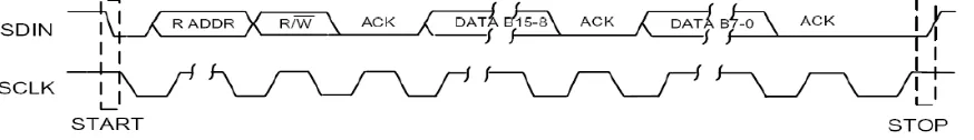
Figure (3) shows the complete requirement of data transmission through I2C .Within the procedure of the I2C bus,
unique situations arise which are defined as START (S) and STOP (P) conditions. START means a HIGH to LOW transition on the SDIN line while SCLK is HIGH and STOP means a LOW to HIGH transition on the SDIN line while SCLK is HIGH .The master always generates START and STOP conditions. The bus is considered to be busy after the START condition. The bus is considered to be free again a certain time after the STOP condition. The bus stays busy if a repeated START (Sr) is generated instead of a STOP condition. In this respect, the START (S) and repeated START (Sr) conditions are functionally identical. Detection of START and STOP conditions by devices connected to the bus is easy if they incorporate the necessary interfacing hardware. The content s of the data line are sent in the same order as seen in figure(3) (after a start condition): 'RADDR', 'R/W', 'ACK','DATAB[15-9]', and 'DATAB[8-0]', which stand respectively for “base address”, “Read/Write”, “acknowledge”, “control address”, and “control data”. The clock for the control serial data input is SCLK. The maximum frequency for this signal is 400 kHz, the frequency used in this paper is f=50 MHz/128 = 390.625 kHz. The data input signal is SDIN, it contains the information for the control interface [Carlos, et al (2007)] .The controller was reprogrammed using the 2-wire
interface with the EP2C35F672C6 FPGA in Cyclone II board. After the start condition that is a falling edge on SDIN while SCLK is high. The following seven bits determines which device receives the data, the address depends on the CBS state (set to ground in this codec) so it is “0011010”. After this address, the bit R/W determines the direction of data transfer, in this case a ‘0’indicates ‘write’. The device recognizes the address and R/W by pulling SDIN low during the ninth clock cycle, acknowledging the data transfer. The control follows with two bit blocks (separated with another acknowledge) the first block B [15:9] contains the control address bits, and the second block B [8-0] contains the control data bits. The stop condition after the data transfer is a rising edge on SDIN when SCLK is high. If a start condition is detected out of the sequence at any point in the data transfer then the device will jump to the idle condition. After a complete control operation, the audio codec returns to the idle state and waits for another start condition.
Fig. 3 Data transmission requirement of I2C
3.3 Wolfson Audio codec WM7831
The WM8731 or WM8731L (WM8731/L) are low power stereo CODECs with an integrated headphone driver. The WM8731/L is designed specifically for portable MP3 audio and speech players and recorders. The WM8731 is also ideal for CD-RW machines and DAT recorders. Stereo 24-bit multi-bit sigma delta ADCs and DACs are used with oversampling digital interpolation and decimation filters. Digital audio input word lengths from 16-32 bits and sampling rates from 8 kHz to 96 kHz are supported [Wolfson (2004)] .The device is controlled via a 2 or 3 wire serial interface. The interface provides access to all features including volume controls, mutes, de-emphasis and extensive power management facilities. The device is available in a small 28- pin SSOP package or the smaller 28 lead quad flat leadless package (QFN).The complete register map is shown in Table.2 [Wolfson (2004)] .There is 11 registers with 16 bits per register (7 bit address + 9 bits of data). These can be controlled using either the 2 wire or 3 wire controller interfaces [Zeyad and et al, (2009)]. Design configure the register R4 of the codec for the
required setting design is very flexible for the configuration of another register
B[15-9] → Control Address = 0000100
B[8-0] → Control Data = 000001101
4. Designing of Serial Transmission Controller
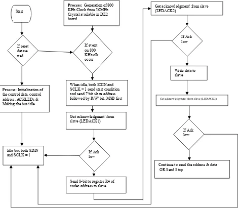
Vol. 2(10), 2010, 5526-5533 to do next. The state variable declared using the SIGNAL keyword is the state memory. It is of type STD_LOGIC_VECTOR, which is an 8-bit bit string. The PROCESS block specifies that whenever there is a change in either of the two signals, clk and rst, the statements inside the block will be executed in sequential order starting with the first line. We have an active high reset signal as specified in the IF statement that tests for the signal being a 1. When rst is deasserted, i.e., when rst is equal to 1, the module goes into the reset mode and outputs logic 1 value for both the SDIN and SCLK output signals. Furthermore, it assigns state x"00" as the initial state for when the FSM starts. x"00" is the syntax for the two hexadecimal digits 00. When rst is asserted, the ELSIF statement is executed. The condition, Clock’ EVENT AND Clock = '1', specified inside the ELSIF statement checks for a rising clock edge. So at every rising clock edge, the FSM will go to a new state and a new set of output signals will be generated [Enoch (2008)] .Figure (4) shows the flowchart of the controller design. To get 400kHz for I2C standard; every 2
cycles of 800kHz = 1 I2C cycle by using crystal frequency 50MHz/64 = 781kHz .The clock for the control serial
data input is SCLK maximum frequency for this signal is 400KHz that we are generating from 800KHz clock. The implementation of SDIN signal requires some special attention as it is bidirectional and open drain so to output the logic 1 on this line ,we need to set this to high impedance, to get high impedance we need to use tri-state output and assign to it a ’Z’ value. The condition signal assignment statement use in VHDL program is SDIN <= ‘Z’ WHEN
SDIN01 =’1’ ELSE ‘0’ [Enoch (2008)], [Bhaskar].
Fig. 4 Flow chart of controller design
Write data to slave
Get acknowledgment' fromslave (LEDACK3)
If Ack low
Continue to send the address & data OR Send Stop
Get acknowledgment' from slave (LEDACK2)
If Ack low
Get acknowledgment' from slave (LEDACK1)
If Ack low
Send 8-bit to register R4 of codec address to slave
Process: Initialization of the control data, control address, ACKLEDs & Making the bus idle
Idle bus both SDIN and SCLK = 1
When idle, both SDIN and SCLK = 1 send start condition and send 7-bit slave address followed by R/W' bit, MSB first If reset
deasse rted Start
If event on 800 KHz clk occur
Process: Generation of 800
5. Simulation and Synthesis
5.1 ModelSim- Altera 6.5b (Quartus II 9.1) (Results)
This is a program to simulate VHDL code. The VHDL files are complied, the input signals are forced to the correspondent values and the evolution of the signals is shown in waves and list.
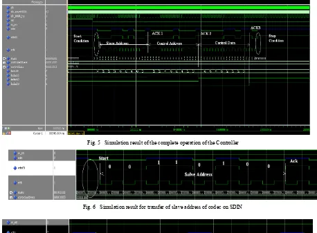
Fig. 5 Simulation result of the complete operation of the Controller
Fig. 6 Simulation result for transfer of slave address of codec on SDIN
Fig. 7 Simulation result for transfer of control Address of codec on SDIN
Vol. 2(10), 2010, 5526-5533
Fig. 9 Simulation result of Ack, Stop condition & idle stage of I2C
5.2 Quartus II (9.0) Sp2 Web Edition (Results)
This is the main program and it is used to build the projects. It has many tools to prepare VHDL or VERILOG structures and download them to the board. The assignment of the pins is done with the Assignment Editor, after
this the VHDL files can be compiled and downloaded to the board with the Programmer tool. In this project, JTAG
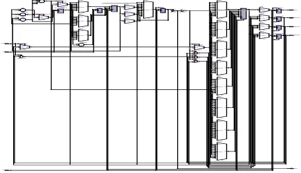
programming (Joint Test Action Group) is used .The configuration bit stream is downloaded directly into the FPGA that will retain the configuration as long as the power is applied to the board. Pin assignment used in the design and experimental results is as shown in figure (10). Synthesized Design of the Controller. (RTL view) is as shown in figure (11).
Fig. 10 Experimental result of designed controller by obtaining Ack from salve device
Fig. 11 Synthesized Design of the Controller. (RTL view)
Results and Discussion
This paper demonstrates the controller’s operation by having its communication with codec connected on the I2C
bus as slave. The design is general enough so that anyone can use another FPGA by changing hardware dependent pin mapping. The authors would like to thank our GOD, friends & our country INDIA.
+ A [4..0] B [4..0] ADDER + A [6..0] B [6..0] ADDER
DPREQ ENA CLR D ENA Q PRE CLR DPREQ
ENA
CLR BUF (DIRECT)
0 1 1 D ENA Q PRE CLR 0 1 1 0 1 D ENA Q PRE CLR 0 1 1 D ENA Q PRE CLR < CIN A [4..0] B [4..0] LESS_THAN 1 < A [6..0] B [6..0] LESS_THAN < A[6..0] B[6..0] LESS_THAN SEL[2..0] DATA[7..0]OUT MUX SEL[2..0] DATA[7..0]OUT MUX SEL[2..0] DATA[7..0]OUT MUX SEL[7..0] DATA[255..0]OUT MUX SEL[7..0] DATA[255..0]OUT MUX SEL[7..0] DATA[255..0]OUT MUX SEL[7..0] DATA[255..0]OUT MUX SEL[7..0] DATA[255..0]OUT MUX SEL[7..0] DATA[255..0]OUT MUX SEL[7..0] DATA[255..0]OUT MUX SEL[7..0] DATA[255..0]OUT MUX SEL[7..0] DATA[255..0]OUT MUX SEL[7..0] DATA[255..0]OUT MUX SEL[7..0] DATA[255..0]OUT MUX SEL[7..0] DATA[255..0]OUT MUX SEL[7..0] DATA[255..0]OUT MUX SEL[7..0] DATA[255..0]OUT MUX SEL[7..0] DATA[255..0]OUT MUX SEL[7..0] DATA[255..0]OUT MUX D ENA Q PRE CLR D ENA Q PRE CLR IO_BUF (TRI)
0
DPREQ
ENA CLR SEL DATAA DATAB OUT0 MUX21 SEL DATAA DATAB OUT0 MUX21 SEL DATAA DATAB OUT0 MUX21 SEL DATAA DATAB OUT0 MUX21 Add0 1' h0 1' h1 5' h0D
-Add1 7' h01
-bcount[2..0] CLK_800k_Hz
clk_count800k[6..0] com b~0
LEDACK1~0 LEDACK1~reg0 LEDACK2~0 LEDACK2~1 LEDACK2~reg0 LEDACK3~0 LEDACK3~reg0 Les s Than0
4' h0 1' h0
-Les s Than1 7' h40
-Les s Than2 7' h20
-Mux1 8' h08
--Mux2 8' h0D
--Mux3 256' hFFF FFFFF FFFFF FFFFF FFFFF FFFFFF FFFFF FFFFF FFFFF FFFFFF FFFFF FFFFF 556B
-Mux5 1' h1 1' h0 1' h0 1' h0 3' h0 3' h0 5' h00
--Mux6 1' h1 1' h0 1' h0 1' h0 3' h0 3' h0 5' h00
--Mux7 1' h1 1' h1 1' h1 1' h0 3' h0 3' h0 5' h00
--Mux8 1' h0 1' h0 1' h0 5' h10 3' h0 6' h00
--Mux9 1' h1 1' h1 1' h1 5' h1F 1' h1 1' h1 5' h00
--Mux10 1' h1 1' h1 1' h1 3' h7 1' h1 1' h0 1' h0 2' h3 3' h0
--Mux11 1' h1 1' h1 1' h1 3' h7 1' h0 1' h1 1' h0 2' h2 3' h6
--Mux12 1' h0 1' h1 1' h1 1' h1 3' h2 3' h2 5' h15 --Mux13
1' h1 -Mux14 1' h1
-Mux16 Mux17 Mux18 SCLK~reg0 SDIN01 SDIN~0 s tate[7..0] bcount~[2..0]
3' h7
-clk_count800k~[6..0] 7' h00
-s tate~[7..0] 8' h0B
-s tate~[15..8] 8' hEE --Clk Rs t LEDACK1 LEDACK2 LEDACK3 SCLK SDIN W_En Mux15 1' h1
-Mux0 8' h34
--Mux4 241' h1FFFFF FFFFFF FFFFF FFFFF FFFFF FFFFF FFFFFF FFFFF FFFFF FFFFF FFFEFF FE
--References
[1] Altera DE2 Package “DE2 Development and Education Board”.
[2] Altera user manual (2006) “DE2 Development and Education Board “Version 1.42 .
[3] Bhaskar J, A VHDL Primer, Prentice Hall.
[4] Carlos Asmat ,David López ,Sanzo Kanwen (2007) “Speech Recognition Using FPGA Technology “June 18, Department of Electrical
Computer and Software Engineering
[5] Enoch Hwang (2008) “Implementing an I2C Master Bus Controller in a FPGA for Maxim DS3232”, April.
[6] Philips Semiconductors (2003) AN10216-01 I2C MANUAL March 24,
[7] Wolfson Microelectronics. (2004) “WM8731 Data sheet”. PDF Document.
[8] Zeyad Assi Obaid, Nasri Sulaiman and M. N. Hamidon (2009) “FPGA-based Implementation of Digital Logic Design using Altera DE2
![Fig. 1 Block Diagram of DE2 Board [Altera (2006)]](https://thumb-us.123doks.com/thumbv2/123dok_us/9616822.1489902/3.612.194.432.356.507/fig-block-diagram-of-de-board-altera.webp)