A Sub-1V High-PSRR Piecewise-Linear
Bandgap Reference
Qianneng Zhou
College of Electronic Engineering, Chongqing University of Posts and Telecommunications, Chongqing, China Email: [email protected]
Qi Li, Hongjuan Li, Jinzhao Lin, Yu Pang, Guoquan Li, Lu Deng Chongqing University of Posts and Telecommunications, Chongqing, China
Email: {lihj1, pangyu}@cqupt.edu.cn
Abstract—A piecewise-linear bandagp reference (BGR) with high power supply rejection ratio (PSRR) and low temperature coefficient is designed for analogue and mixed signal systems in this paper. By adopting LDO regulator, the designed high PSRR piecewise-linear BGR achieves well performances and has a simple architecture. Simulation results show that the PSRR of the designed piecewise-linear BGR with LDO regulator at 10Hz, 1kHz and 100kHz achieves, respectively, -110.42dB, -109.18dB and -64.51dB. Compared to the designed BGR without LDO regulator, the PSRR of the designed high PSRR piecewise-linear BGR with LDO regulator has the improvements of about 35dB, 36.9dB and 29.28dB at 10Hz, 1kHz and 100kHz respectively. The designed piecewise-linear BGR with LDO regulator generates an output voltage of 0.68V with 1.65ppm/ºC temperature coefficient in the range from -50 ºC to 125 ºC. The deviation of the output voltage is within 98.23μV when the power supply voltage VDD changes from 1.2V to 7V.
Index Terms—bandgap reference (BGR), piecewise-linear, LDO regulator, power supply rejection ratio (PSRR)
I. INTRODUCTION
Bandgap reference (BGR) is a very important block for many analogue and mixed signal electronic devices such as data converters, DC-DC converters, DRAMs, linear regulators and so on. The BGR should be independent of fluctuations of power supply voltage and temperature, and also be implemented without modification of fabrication process. In modern CMOS technology, the output voltage of BGR is usually a weighted sum of the forward-bias emitter-base voltage of diode-connected parasitic vertical PNP transistor and the thermal voltage [1]. Conventional BGR has a large temperature coefficient over the whole temperature range and cannot meet the requirements of high precision circuits. To improve the temperature performance of BGR, many temperature compensation techniques have been reported, such as correlated double sampling technique [2], curvature correction [3-6] and so on. Recently, demands for low-voltage BGR circuits have increased enormously because they are widely used in portable electronic applications. Simultaneously, the most significant noise
injected to the output of BGR circuit is the supply noise regarding to the other noise. On the other hand, a high power supply rejection ratio (PSRR) BGR is desired to achieve high performance analogue and mixed signal systems, particularly in wireless communications. Therefore, a BGR structure, which has high PSRR over broad frequency range, should be chosen to reject the supply noise coupled from the high-speed digital circuit on the chip.
In the recent past, many approaches have be developed to improve the PSRR of BGR, such as supply independent current source technique [7], pre-regulator technique [8-11], subtractor technique [12], pseudo floating voltage source technique [13], cascode current-mode technique [14], self-cascode current mirror technique [15], low dropout (LDO) regulator technique [16], voltage follower technique with PMOS as input transistor [17] and so on. In general, these reported BGR with PSRR enhancement have achieved well performance. However, to further improve the performance of BGR, the high PSRR BGR structure must still be analyzed and discussed.
In this paper, a high PSRR CMOS BGR with less than 1V output voltage is designed and analyzed. Employing an improved piecewise-linear temperature compensation technique and a LDO regulator, the designed BGR achieves a high PSRR performance over a wide frequency range and a well temperature characteristic over a wide temperature range. The analysis and design of piecewise-linear BGR without LDO regulator will be given in Section II. Section III will discuss the high PSRR piecewise-linear BGR with LDO regulator. Simulation results are described in Section IV. Finally, conclusions are given in Section V.
II. ANALYSIS AND DESIGN OF PIECEWISE-LINEAR BGR
M1 M 2
A1 A2
M3 M 4
M5
M6
M7 M8
M9
M10
M11
Q1 Q2
R1
R2
R3
R4
A B C
(a) (b)
VREF
IPTAT
ICTAT
IPTAT
ICTAT INL
Ms1
Ms2
Ms3
Ms5
Ms4
VDD
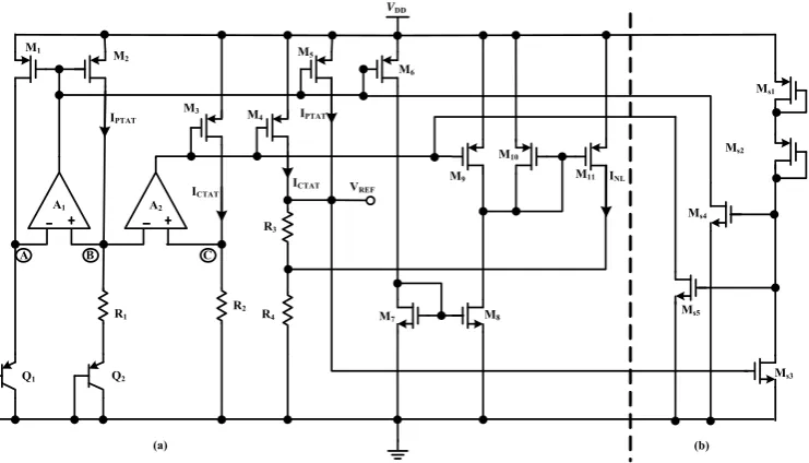
Figure 1. Designed BGR (a) core circuit of BGR, (b) start-up circuit
Temperature
Vol
tag
e
Tr
VPTAT
VCTAT
VREF
VNL
Figure 2. Operation of designed BGR
voltage VREF and has a good temperature characteristic. At the same time, all MOS transistors adopt the long channel transistor so that the channel-length modulation effect is negligibly small in this paper.
For convenience, it is assumed that Wj, Lj and Ij are, respectively, channel-width, channel-length and drain current of transistor Mj in this paper, here j=1, 2, 3…. The core circuit of piecewise-linear BGR consists of transistors M1~M11, bipolar transistors Q1 and Q2, resistors R1~R4, and amplifiers A1 and A2. Amplifiers A1 and A2 are entirely the same, and their dc gain Ad has that Ad>>1. Amplifier A1 forces the voltages VA and VB be equal, and amplifier A2 forces the voltages VB and VC be equal, i.e. VA=VB=VC=VEB1. Here, VA, VB, VC and VEB1 are, respectively, the voltages of node A, node B, node C and emitter-base voltage of Q1. Transistors M1, M2 and M5 are entirely the same, and Q2 has an emitter area that is m times that of Q1. So, the drain currents of transistors M2 and M5 can be derived as
2 5
1
1
ln
kT
I
I
m
q R
= =
(1)where, k is Boltzmann’s constant, q is electronic charge, and T is absolute temperature. It is concluded that currents I2 and I5 are proportional to the absolute temperature T. Amplifier A2 force voltages VB and VC be equal, and transistors M3 and M4 are entirely the same. Therefore, the drain currents of M3 and M4, i.e. I3 and I4, can be derived as
1 3 4
2
EB
V
I
I
R
= =
(2)VEB1 has a negative temperature coefficient, so it is concluded that currents I3 and I4 have a negative temperature coefficient. Transistors M2 and M6 have the same aspect ratio, and M3 and M9 have also the same aspect ratio. Therefore, it is concluded that I6=I2 and I3=I9.
Transistorss M7 and M8 form the current-mirror pair, and transistor M8 has the aspect ratio that is α times that of transistor M7. By optimizing the value of parameter α, it can be achieved that I9=I8=αI2 under the condition of room temperature Tr. Therefore, the following expression can be derived as
1
8 9
1 2
1
8 9
1 2
1
8 9
1 2
1
ln
,
1
ln
,
1
ln
,
EB
r
EB
r
EB
r
V
kT
I
m
I
when T
T
q R
R
V
kT
I
m
I
when T
T
q R
R
V
kT
I
m
I
when T
T
q R
R
α
α
α
⎧
=
< =
<
⎪
⎪
⎪⎪
=
= =
=
⎨
⎪
⎪
=
> =
>
⎪
⎪⎩
(3)
M1 M 2
A1
A2
M3
M4
M5
M6
M7 M8
M9
M10
M11
Q1
Q2
R1
R2
R3
R4
A B
(a) (d)
VREF
IPTAT
ICTAT
IPTAT
ICTAT
INL
Ms1
Ms2
Ms3
Ms5
Ms4
VDD
` `
MDS1
MDS2
MDS3
MDS4
MB1 MB2
MB3
MB4
RB1
MD1
MD2 MD3
MD4 MD5
MD6
MD7
MPASS
RD1
CD1
RFB1
RFB2
CD2
CD3
`
(b) (c)
VREG
VBIAS
V1
VREG
VFB
1
C 2 V2
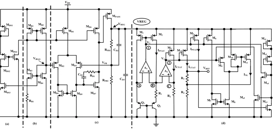
Figure 3. Designed high PSRR BGR with LDO regulator (a) start-up circuit, (b) supply-independent bias circuit, (c) LDO regulator, (d) core circuit of piecewise-linear BGR
1
1 3
0,
1
ln
,
NL r
EB
NL r
I
when T
T
V
kT
I
m
when T
T
q R
R
α
=
≤
⎧
⎪
⎨
=
−
>
⎪⎩
(4)So, the output voltage VREF of piecewise-linear BGR can be derived as
1
3 4 4
1 2
1
(
)(
ln
EB)
REF NL
PTAT CTAT NL
V
kT
V
R
R
m
R I
q R
R
V
V
V
=
+
+
+
=
+
+
(5)
3 4
1
1
(
)
ln
PTAT
kT
V
R
R
m
q R
=
+
(6)1 3 4
2
(
)
EBCTAT
V
V
R
R
R
=
+
(7)4
NL NL
V
=
R I
(8) According to (1) ~ (8), it is concluded that VPTAT, VCTAT and VNL are, respectively, the voltages with positive-temperature coefficient, negative-temperature coefficient and piecewise temperature coefficient, and their relations are shown in Fig.2. Equation (5) shows that the piecewise-linear BGR can achieve a low temperature coefficient bandgap reference voltage VREF by optimizing resistors R1~R4 and parameter α in theory. However, the operating supply voltage of piecewise-linear BGR, which is shown in Fig.1, is the power supply voltage VDD, and it cannot achieve high PSRR over a wide frequency range. Therefore, the piecewise-linear BGR cannot be effectively applied to analogue and mixed signal systems that have the requirement of high PSRR. Therefore, to further improve PSRR of BGR, a high PSRR piecewise-linear BGR is designed by adopting LDO regulator in this paper, and will be analyzed in Section III.III.ANALYSIS AND DESIGN OF HIGH PSRRPIECEWISE
-LINEAR BGR
Fig.3 shows the designed high PSRR piecewise-linear BGR, and all MOS transistors adopt the long channel transistor so that the channel-length modulation effect is negligibly small. The designed high PSRR piecewise-linear BGR consist of a start-up circuit, a supply-independent bias circuit, a LDO regulator and a core circuit of piecewise-linear BGR. The core circuit of piecewise-linear BGR is entirely the same as that designed in Section II, but whose operating supply voltage is the output voltage VREG of LDO regulator instead of power supply voltage VDD. Therefore, the designed high PSRR piecewise-linear BGR with LDO regulator can achieve an output voltage VREF with low temperature coefficient and high PSRR. The supply-independent bias circuit produces supply-supply-independent bias voltages, and will be discussed in Section III.A. Because there are two possible equilibrium points in the supply-independent bias circuit, a start-up circuit is necessary. MDS1~MDS4 form the start-up circuits, as shown in Fig.3 (a). The function of LDO regulator is to produce an internally regulated voltage VREG that is the operating supply voltage of core circuit of piecewise-linear BGR instead of power supply voltage VDD. The analysis and design of LDO regulator will be given in Section III.B.
A. Supply-Independent Bias Circuit
` `
`
` ` VREG
VDD
RL
Ceq-out
CD2
CD1 R D1
RFB1
RFB2
VBIAS
Co1
Ro1
Ro2 Co2
Mpass
gmd2
gmd7 gmpass
AE1 AE2
VFB
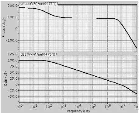
Figure 4. Topologic architecture of LDO regulator
Figure 5. Open-loop frequency response of LDO regulator
2
3 4 2
4 4 1
2
1
1
1
(
)
B B
n ox B B B
I
I
C
W
L
R
N
μ
⎛
⎞
=
=
⎜
−
⎟
⎝
⎠
(9)where, μn is the mobility of an electron, Cox is the gate oxide capacitance per unit area. Equation (9) indicates that the bias-current IB4 is independent of the power supply voltage VDD. Therefore, the gate-voltage VBIAS of MOS transistor MB4 can be derived as
4 4 1
2
1
1
1
(
)
BIAS THN
n ox B B B
V
V
C
W
L
R
N
μ
⎛
⎞
=
⎜
−
⎟
+
⎝
⎠
(10)where, VTHN is the threshold voltage of NMOS transistor. Equation (10) indicates that the bias voltage VBIAS is also independent of the power supply voltage VDD.
B. Analysis and Design of LDO Regulator
The designed LDO regulator is shown in Fig.3 (c), which consists of error amplifier, a PMOS power transistor Mpass, and a feedback resistive network. The feedback resistive network consists of capacitor CD2, and resistors RFB1 and RFB2. The error amplifier consists of MOS transistors MD1~MD7, resistor RD1 and capacitance CD1. The error amplifier compares the reference voltage VBIAS, which is provided by the supply-independent bias circuit, with the feedback voltage VFB that is provided by the feedback resistors RFB1 and RFB2, and generates an error voltage signal which is fed into the gate of power transistor Mpass to change its over-drive. The over-drive adjusts the drain current of Mpass and forces the output voltage VREG of LDO regulator to be corrected to the proper level. The error amplifier and power transistor Mpass form a negative feedback system, which is equivalent to a three-stage amplifier negative feedback system. Therefore, the open-loop stable of LDO regulator is critical issue.
To analyze the stability of LDO regulator, the open-loop transfer function of LDO regulator should be analyzed and discussed. For convenience, the topologic architecture of LDO regulator is shown in Fig.4. The first-stage error amplifier AE1 consists of MOS transistors MD1~MD5, whose equivalent input transconductance is written as gmd2. The second-stage amplifier AE2 consists of MOS transistors MD6 and MD7, whose equivalent input transconductance is written as gmd7. Ro1 and Ro2 are the
output resistance of amplifier AE1 and AE2 respectively, and Co1 and Co2 are the parasitic capacitances at the output of AE1 and at the gate of Mpass respectively. gmpass is the equivalent transconductance of Mpass, and RL is the equivalent load resistance. In Fig.4, Ceq-out=CD3+CL, here CL is the equivalent capacitance of internal power line.
To simplify the transfer function without losing accuracy with the goal of providing a clearer insight into the designed LDO regulator structure, it is assumed that capacitors CD1, CD2 and Ceq-out are much greater than the parasitic capacitance Co1 and Co2, and the gains of each stage is much greater than one, i.e. gmd2Ro1, gmd7Ro2 and gmpassRL>>1. On the other hand, the feedback resistance RFB2 is much greater than the load resistance RL, and Ro1 and Ro2 are greater than RD1. Therefore, the loop transfer function of the designed LDO regulator can be approximated to
0 1
2
3 1 2 2 3
( )
(1
)(1
)
(1
)(1
)(1
)(1
)
loop
f
dB f
T
s
T
s z
s z
s
s
s
s
s
p
−p
p
p p
p
+
+
=
+
+
+
+
+
(11)
2
0 2 1 7 2
2 1
FB
md o md o mpass L
FB FB
R
T
g
R g
R g
R
R
R
=
+
(12)3
7 1 2 1
1
dB
md o o D
p
g
R R C
−
=
(13)1
1
eq out L
p
C
−R
=
(14)2 2
1 2
m
o o
g
p
C
C
=
+
(15)3
1 1 2
1
(
//
)
D o o
p
R
C
C
2 1 2
1
(
//
)
f
D FB FB
p
C
R
R
=
(17)1
1 1 7
1
(
1
)
D D md
z
C
R
g
=
−
(18)1 2
1
f FB Dz
R
C
=
(19)Co1 and Co2 are the lumped capacitance, so the non-dominant poles p2 and p3 will shift to a higher frequency than the unity-gain frequency (UGF). To cancel the effect of non-dominant poles in the designed LDO regulators, the zero zf should be lower than poles p1 and pf, so RFB2 should be much smaller than RFB1, i.e. zf<<pf. That is to say, the effect of the pole p1 can be cancelled by zf. To ensure z1 be left-plane zero, RD1 should be selected much larger than 1/gmd7. At the same time, since CD1 and CD2 are the compensation capacitor, it is practical to take the assumption of z1<pf by optimizing resistors RD1 and RFB1, and compensation capacitors CD1 and CD2. From the above discussion, the LDO regulator will be stable because it is similar to a single pole system. Fig.5 shows the simulated open-loop frequency response of the designed LDO regulator. Simulation results show that the phase margin is about 61º, which is sufficient to ensure the loop stability of LDO regulator.
C. Analysis of PSRR
To improve the PSRR of piecewise-linear BGR, a LDO regulator is adopted in this paper, as shown in Fig.3. The operating supply voltage of core circuit of piecewise-linear BGR is the output voltage VREG instead of power supply voltage VDD. Therefore, the PSRR of piecewise-linear BGR with LDO regulator will be improved. Under the condition of low frequency, the PSRR can be quantitatively analyzed as follows.
For convenience, it is assumed that gmj and imj are, respectively, the transconducatnce and the small-signal drain current of transistor Mj, here j=1, 2, 3…. Assumed that power supply voltage has an incremental variation vdd, the incremental current ib1 of MB1 can be derived as
1
3 1 3 1
1
dd b
mb B dsb
mb
v
i
g
R r
g
=
+
(20)
where, rdsb3 is the source-drain resistance of MB3. MB1 and MB2 form current mirror pair, and they are entirely the same. Therefore, the gate-source variation vbias of MB4 can be derived as
4 3 1 3
1
1
(
)
dd bias
mb mb B dsb
mb
v
v
g
g
R r
g
=
+
(21)
Assumed that vreg is the output voltage variation of LDO regulator, and the feedback voltage variation vfb can be derived as
2 1 2 reg fb FB FB FB
v
v
R
R
R
=
+
(22)As shown in Fig.3, the error amplifier of LDO regulator is made up of MOS transistors MD1~MD7, resistor RD1 and compensation capacitor CD1. To simple the analysis, it is assumed that the dc gain Av of error amplifier is far greater than 1, i.e. Av>>1. Neglected the effect of drain current variation of MD1 and MD6, the gate voltage variation vgpass of power transistor MPASS can be derived as
2
1 2
4 3 1 3
1
1
(
)
v FB reg v dd
gpass
FB FB
mb mb B dsb
mb
A R
v
A v
v
R
R
g
g
R r
g
=
−
+
+
(23) According to (20) ~ (23) and the Kirchhoff current law (KCL) at the output node VREG of the LDO regulator, it is derived as
4 3 1 3
1 2 1 2
1
1
(
)
1
vmb mb B dsb
reg mb
mpass eq L
v FB dd
mpass eq L
FB FB
A
g
g
R r
v
g
g
R
A R
v
g
R
R
R
− −+
+
=
+
+
(24) where, Req-L is the equivalent resistance seen from node VREG to ground. In the similar way, it is assumed that va, vb and v1 are, respectively, the voltage variations at node A, node B and node 1. So, va and vb can be derived as1
(
- )r
1a m reg a
v
=
g
v
v
(25)2
(v - )r
1b m reg b
v
=
g
v
(26) where, ra and rb are the resistance seen from node A and node B to ground respectively. Amplifier A1 and A2 are entirely the same, and whose dc gain Ad is far greater than 1, i.e. Ad>>1. In Fig.3, the voltage variation v1 at node 1 has that v1=Ad×(vb-va). According to (25) and (26), it is derived as1 reg 1 1
1+
d m d mA g
v
v
A g
β
β
=
(27)where, β=rb-ra. MOS transistors M1, M2, M5 and M6 are entirely the same, and it is concluded that gm1=gm2=gm5= gm6. Therefore, it is derived as
1,2,5,6 1 1
1
1+
m reg d mi
g
v
A g
β
=
(28)The voltage variation v2 at node 2 has that v2=Ad×(vc -vb), here vc is voltage variation at node C. MOS transistors M3, M4 and M9 are entirely the same, and it is concluded that gm3=gm4=gm9. In the similar way, it is derived as
1 1
3,4,9 3 reg
1 4 2
1+
(1+
)(1
)
d m d m b
m
d m d m
A g
A g r
i
g
v
A g
A g R
β
β
+
=
+
(29)Figure 6. Output voltage VREF of piecewise-linear BGR with- and
without- LDO regulator as a function of temperature T
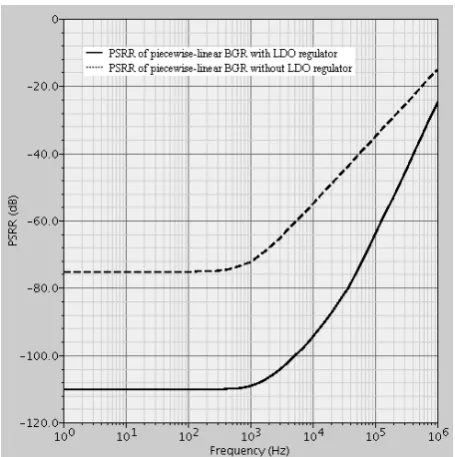
Figure 7. Simulated PSRR of piecewise-linear BGR with- and without- LDO regulator
of transistor M7. Transistors M10 and M11 are entirely the same, so it is derived as
11 1
1
1 1
3 reg
1 4 2
1
1+
1+
(1+
)(1
)
m reg
d m
d m d m b
m
d m d m
i
g
v
A g
A g
A g r
g
v
A g
A g R
α
β
β
β
=
+
−
+
(30)
To simple the analysis, it is assumed that
1
1
d m
A g
β
>>
andA g R
d m4 2>>
1
. According to (28) ~ (30) and KCL at the output of BGR, it is derived as3 4
3
reg 2
(1
)
ref b
d d
v
r
R
R
R
v
A R
A
β
α
β
β
+
+ +
≈
+
(31)where, vref is the output voltage variation of piecewise-linear BGR with LDO regulator. Therefore, the PSRR of the designed piecewise-linear BGR with LDO regulator can be written as
20lg
20lg
20lg
20lg
ref ref reg
dB
vdd reg dd
ref reg
reg dd
v
v
v
PSSR
v
v
v
v
v
v
v
=
=
×
=
+
(32)
According to (24), (31) and (32), it is concluded that the PSRR of the designed piecewise-linear BGR will be improved significantly by adopting the LDO regulator.
IV.SIMULATION RESULTS
To confirm the circuit of the designed piecewise-linear BGR in this paper, the piecewise-linear BGRs with- and
without- LDO regulator are designed and simulated in SMIC 0.18μm CMOS process with 1.35-V power supply voltage.
Fig.6 shows the output voltage VREF of piecewise-linear BGR with- and without- LDO regulator as a function of temperature T with 1.35-V power supply voltage. Simulation results show that the temperature coefficient of the piecewise-linear BGR without LDO regulator is 2.89ppm/ºC when temperature varying from -50 ºC to 125 ºC. And, the output voltage VREF of piecewise-linear BGR with LDO regulator has only the temperature coefficient of 1.65ppm/ºC.
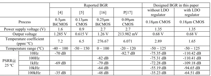
The simulated PSRR of piecewise-linear BGR with- and without- LDO regulator is shown Fig.7. The piecewise-linear BGR with LDO regulator at 10Hz, 100Hz, 1kHz, 10kHz and 100kHz achieves , respectively, 110.42dB, 110.41dB, 109.18dB, 94.65dB and -64.51dB. And the piecewise-linear BGR without LDO regulator at 10Hz, 100Hz, 1kHz, 10kHz and 100kHz achieves, respectively, 75.35dB, 75.31dB, 72.28dB, -55.19dB and -35.23dB. Compared to the piecewise-linear BGR without LDO regulator, the designed high PSRR piecewise-linear BGR with LDO regulator has an improvement of PSRR with about 35dB, 36.9dB and 29.28dB at 10Hz, 1kHz and 100kHz respectively. Therefore, the PSRR improvement is achieved by adopting LDO regulator.
Figure 8. Simulated line-regulation of piecewise-linear BGR with- and without- LDO regulator
LDO regulator has a well line regulation. Finally, to provide an evaluation on the designed high PSRR BGR with LDO regulator in this paper, comparison of some reported BGR is shown in Table I. As shown in Table I, the designed piecewise-linear BGR with LDO regulator has a well performance.
V. CONCLUSIONS
A CMOS high PSRR piecewise-linear BGR, which has an output below 1V, has been designed and analyzed in this paper. Compared to piecewise-linear BGR without LDO regulator, the designed high PSRR piecewise-linear BGR achieves high PSRR performance by adopting LDO regulator. Simulation results shows that the designed high PSRR piecewise-linear BGR with LDO regulator
provides an output voltage with excellent stability, a low temperature coefficient, and high PSRR performance. It is well suited for analogue and mixed signal systems.
ACKNOWLEDGMENT
This work was supported in part by a grant from National Science Foundation of China (Grant No. 61102075, and 61301124), Natural Science Foundation Project of CQ CSTC (Grant No. CSTCJJA40011 and CSTC2010BB2412), Science and Technology Research Project of Chongqing Education Commission (Grant No. KJ120503, KJ120507, and KJ120533), Dr. Start Fund of Chongqing University of Posts and Telecommunications (Grant No.A2010-09), 2013 University Innovation Team Construction Plan Funding Project of Chongqing, and Special Project of Internet of Things from Ministry of Industry and Information Technology, Chongqing Development Plan of Innovative Young Talents (Grant No. cstc2013kjrc-qnrc0126).
REFERENCES
[1] G. A. Rincon-Mora, P. E. Allen, “A 1.1-V current-mode and piecewise linear curvature corrected bandgap references,” IEEE J. Solid-State Circuits. vol.33, p.
1551-1554, October 1998.
[2] P. Y. Chen, S. J. Chang, C. M. Huang, and J. F. Lin, “A 1-V bandgap reference without on-chip resistors,” IEEE Asia Pacific Conference on Circuits and Systems. pp. 160-163,
Kaohsiung, December 2012.
[3] P. B. Basyurt, D. Y. Aksin, “Design of a curvature-corrected bandgap reference with 7.5ppm/C temperature coefficient in 0.35μm CMOS process,” IEEE International Symposium on Circuits and Systems. pp. 3142-3145, Seoul,
May 2012.
[4] Z. K. Zhou, Y. Shi, Z. Huang, P. S. Zhu, Y. Q. Ma, Y. C. Wang, Z. Chen, X. Ming, and B. Zhang, “A 1.6-V 25-mA 5-ppm/°C curvature-compensated bandgap reference,”
IEEE Trans. Circuits Syst. I, Reg. Papers. vol. 59, pp.
677-684, April 2012.
[5] C. M. Andreou, S. Koudounas, and J. Georgiou, “A novel wide-temperature-range, 3.9ppm/ºC CMOS bandgap reference circuit,” IEEE J. Solid-State Circuits. Vol. 47, pp.
574-581, February 2012.
TABLE I.
PERFORMANCE SUMMARY OF BANDGAP REFERENCE
Reported BGR Designed BGR in this paper
[4] [5] [16] P[17] without LDO regulator with LDO regulator
Process BiCMOS 0.5μm 0.13CMOS μm BiCMOS0.25μm 0.09CMOS μm 0.18μm CMOS 0.18μm CMOS
Power supply voltage (V) 1.6 0.9 2.7 2.7 1.35 1.35
Output voltage 1.285 V 0.615 V 1.26 V 213.982 mV 0.68 V 0.68 V
Temperature coefficient
(ppm/ ºC) 7.2 6.5 276.67 6.071 2.89 1.65
Temperature range (ºC) -40 ~ 100 -50 ~ 150 0 ~ 100 -20 ~ 120 -50 ~ 125 -50 ~ 125
PSRR@ 25 ºC
10Hz -70 dB -82.7 dB -75.35 dB -110.42 dB
100Hz -82 dB -75.31 dB -110.41 dB
1kHz -69 dB -79 dB -72.28 dB -109.18 dB
10kHz -64 dB -55.19 dB -94.65 dB
[6] S. Sano, Y. Takahashi, M. Horiguchi, and M. Ota, “A sub-1V 3.9mW bandgap reference with a 3σ inaccuracy of ±0.34% from -50°C to +150°C using piecewise-linear-current curvature compensation,” International Symposium on VLSI Circuits. pp. 22-23, Honolulu, June 2012.
[7] S. Mechrmanesh, M. B. Vahidfar, and H. A. Aslanzadeh, M. Atarodi. “A 1-volt, high PSRR, CMOS bandgap voltage reference,” IEEE International symposium on circuits and systems. vol. 1, pp. I-381-I-384, Bangkok,
May 2003.
[8] Y. Hu, and M. Saean, “A 900mV 25μW high PSRR CMOS voltage reference dedicated to implantable micro-devices,” IEEE International symposium on circuits and systems. vol. 1, pp. I-373-I-376, Bangkok, May 2003.
[9] D. Xiao, W.M. Li, X.F. Zhu, and X.D. Fu, “A curvature-compensated bandgap reference with improved PSRR,”
6th International conference on ASIC. vol.2, pp. 548-551,
Shanghai, October 2005.
[10]Z.H. Ning, L.N. He, Y. Wang, and Y.L. Shao, “A novel high PSR voltage reference with secondary temperature compensation,” International conference on electrical and control engineering. Vol.3, pp. 3200-3203, Wuhan, May 2010.
[11]X.Z. Knang, Z.W. Tang, “A novel high PSRR bandgap over a wide frequency range,” International conference on solid-state and integrated circuit technology. pp. 418-420, Beijing, October 2010.
[12]J. Yu, Y.F. Zhao, Z.M. Wang, and T.L. Zhang, “A curvature-compensated bandgap reference with high PSR,”
International conference granular computing. pp. 752-755, Hangzhou, August 2008.
[13]H.Y. Zhang, P.K. Chan, and M.T. Tan, “A high PSR voltage reference for dc-to-dc converter applications,”
International symposium on circuits and systems. vol. 1, pp.
816-819, Taipei, May 2009.
[14]A. Dey, and T.K. Bhattacharyya, “A CMOS bandgap reference with high PSRR and improved temperature stability for system-on-chip applications,” International conference of electron devices and solid-state circuits. pp.
1-2, Tianjin, November 2011.
[15]T.L. Cao, Y. Han, X.P. Liu, H. Luo, and H. Zhang, “A 0.9-V high-PSRR bandgap with self-cascode current mirror,”
International conference on circuits and systems. vol.1, pp.
267-271, Kuala Lumpur, October 2012.
[16]L. Lei, L. Lukas, A. Aytac, S. Sebstian, W. Ralf, and H. Stefan, “A low power bandgap voltage reference circuit with PSRR enhancement,” 8th International conference on Ph.D. research in microelectronics and electronics. pp.
213-216, Aachen, June 2012.
[17]K.P. Francisco, J.A. Hora, “Very low bandgap voltage reference with high PSRR enhancement stage implemented in 90nm CMOS process Technology for LDO application,”
International conference on electronics design, systems and applications. pp. 216-220, Malaysia, November 2012.
[18]B. Razavi, Design of Analog CMOS Integrated Circuits,
McGraw-Hill, 2001.
QiannengZhou received the B.S. degree, the M.Sc degree, and Ph.D degree, all in microelectronic, from Harbin Institute of Technology (HIT), Harbin, China, in 1998, 2002 and 2009, respectively. Since 2009, he has been an associate professor with Chongqing University of Posts and Telecommunications (CQUPT). His current interests include dc-dc converters, amplifiers, LDO regulator and LED drivers.
Qi Li received the B.S. degree in microelectronic from Chongqing University of Posts and Telecommunications (CQUPT), Chongqing, China, 2012. She is currently working toward the M.Sc degree at CQUPT. Her research interests include dc-dc converters, and LDO regulator.
Hongjuan Li received the M.Sc degree in School of Automation Engineering from Northeast Dianli Universisty, Jilin, China, in 2006. She is currently a lecturer with Chongqing University of Posts and Telecommunications, Chongqing (CQUPT), China. Her research interests include Embedded System, and RFID system.
Jinzhao Lin received Ph.D degree in 2001 from Chongqing University. Since 2003 he has been a professor with Chongqing University of Posts and Telecommunications (CQUPT). His current interests include wireless communications and ASIC design.
YuPang received Ph.D degree in 2010 from McGill University. Since 2012 he has been an associate professor with Chongqing University of Posts and Telecommunications (CQUPT). His current interests include wireless communications and ASIC design.
Guoquan Li received his Ph.D. degree in College of Communication Engineering from Chongqing University (CQU), Chongqing, China in 2012. He is currently a lecturer with Chongqing University of Posts and Telecommunications, Chongqing (CQUPT), China. His research interests include digital baseband signal processing, multi-user MIMO system, coding theory and technology.