www.wjert.org 81 Leela et al. World Journal of Engineering Research and Technology
DESIGN AND IMPLEMENTATION OF 4 BIT FLASH ANALOG TO
DIGITAL CONVERTER USING LTE AND UNIVERSAL GATE
COMPARATOR
Leela S. Bitla*, Priyanka Gomase and Rupali Shinganjude
Asst. Professor, Priyadarshini Bhagwati College of Engg., PBCOE, Nagpur-09, Maharashtra,
India.
Article Received on 10/01/2016 Article Revised on 01/02/2016 Article Accepted on 25/02/2016
ABSTRACT
This Paper introduces 4 bit flash ADC design using Linear Tunable
Transconductance Element based comparators for high speed and low
powerconsumption using 180nm technology and 90nmtechnology.
Thermometer to binary decoder with low power consumption, less area
& short critical path is selected for the design of low power high speed.
Proposed comparator provides improvedPSRR (Power Supply
Rejection Ratio) compared TIQ (Threshold Inverter Quantizer)
comparator NAND based topology is used which improves PSRR as
well as linearity.
Keywords: CMOS-LTE, CMOS-NAND gate MUX Decoder, ADC, Gain Booster network.
INTRODUCTION
Although the full-flash type A/D converter architecture is the most attractive solution for
high-speed A/D converter designs, from a power dissipation and area perspective.[2] Therefore the comparator structure is the most critical part in full-flash type architecture. The
need arises for ADCs with higher resolution and faster conversion speed. The most popular
type of fast converter is the flash ADC. This architecture required 2N-1 Comparator to achieved N bit resolution. For 4 bit ADC we required 15 comparators. The proposed
improved threshold Inverter can used to preprocess the analog input signals, thus reducing the
number of comparator.
World Journal of Engineering Research and Technology
WJERT
www.wjert.org
SJIF Impact Factor: 3.419*Correspondence for Author
Leela S.Bitla
Asst. Professor,
Priyadarshini Bhagwati
College of Engg., PBCOE,
Nagpur-09, Maharashtra,
India.
www.wjert.org 82 II .Design of Flash ADC
This section describes the design of 4-bit flash ADC. It consists of three blocks: (1)
Comparator bank, and (2) Gain Booster and (3) Decoder.
Figure 1: Block diagram of Flash ADC.
However due to non-ideal effects such as short channel and narrow channel effects, the
above design process cannot be so practical, therefore higher level MOS transistor design is
to be used, therefore effective threshold voltage are re-calculated after the transistor sizing
process to handle these non-ideal effect such as narrow channel effect.[2] The design process can be obtain as below:
1. Design process involve the minimum size inverter which determine the threshold voltage
value of the midpoint Quantizer Qn
Where the value of Wn = Wp we maintain the channel length is kept at minimum value.
2. Determine the analog input voltage range as by the following equation
Analog range = Vdd-( Vtn + |Vtp| )
Where Vtn & Vtp are the threshold voltage for NMOS and PMOS device.[2]
Figure 2: Block diagram of design process
To calculate LSB value like
LSB=Analog range/2n
Then calculate the ideal threshold points for each quantizer consider the center is Qn. the
quantizer of Qn+1…….Qn+p it is called PMOS side,(W/L) is kept at minimum value, The
same process is applicable for NMOS but in opposite way.[2]
Replicate this entire quantizer block & complete the interconnection to get the cascaded
www.wjert.org 83 A. Lte Comparator Flash ADC
The reference voltage are changed when there is a noise in the power supply voltage to
overcome this problem the CMOS LTE comparator are proposed. Where input voltage is
compare with reference voltage to get Logic „1‟ or „0‟.when Vin > Vref then we get logic „1‟
at the output and When Vin< Vref the we get the logic „0‟ at the output of comparator circuit.
This proposed scheme has the following advantages .Use Digital Comparator for high speed
& low power consumption. To increase the voltage gain of the comparator. To reduced the
noise problem & to reduced charge rejection ratio. Power supply voltage & Temperature are
much smaller.
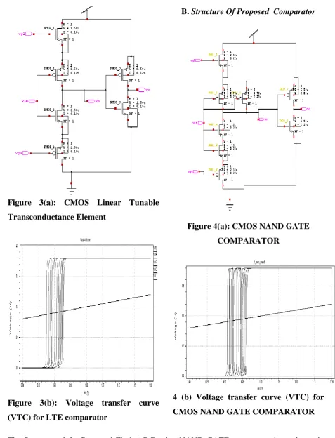
The CMOS-LTE Comparator uses Linear Tunable Transconductance Element and inverter as
shown in Figure(3). The internal reference voltages are generated by systematically varying
the transistor sizes of the CMOS linear tunable transconductance element. All transistor sizes
of this element are identical in this design, with Vg1 and Vg4 as fixed voltages.[1,2] The output of this component is connected to CMOS inverter to increase the voltage gain of the
comparator. Using CMOS-LTE (CMOS Linear Tunable Transcoductance Element)
Comparator. Voltage Transfer characteristics of an Inverter can be calculated mathematically
by equation.[1,2]
Vm =(r(Vdd-│Vtp│)+Vtn) / (1+r)
With
r=(Kp/Kn)1/2
where Vtp and Vtn represent the threshold voltages of the PMOS and NMOS devices
respectively and
Kn = (W/L)n . μn Cox
Kp = (W/L)p . μp Cox
It can be shown that the Vm point on the Voltage transfer curve (VTC).The VTC is set for 15
www.wjert.org 84 Figure 3(a): CMOS Linear Tunable
Transconductance Element
Figure 3(b): Voltage transfer curve (VTC) for LTE comparator
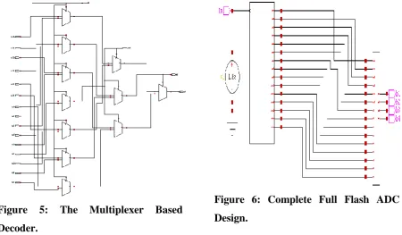
B. Structure Of Proposed Comparator
Figure 4(a): CMOS NAND GATE COMPARATOR
4 (b) Voltage transfer curve (VTC) for CMOS NAND GATE COMPARATOR
The Structure of the Proposed Flash ADC using NAND GATE comparator is as shown in
Figure4(a) By using CMOS-NAND gate comparator we are getting the linearity at the
output as compare with CMOS-LTE Comparator. The gain boosters make shaper threshold of
www.wjert.org 85
C. Gain Booster
Each gain booster consists of two cascaded inverters. The transistor size of each gain booster
is identical The gain booster is used to increase voltage gain of the output of the comparator
so that it provides a full digital output voltage swing.[1,2]
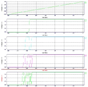
D. The Multiplexer Based Decoder
For an N-bit flash ADC the most significant bit (MSB) of the binary output is high if more
than half of the outputs in the thermometer scale are logic one. Hence MSB is same as the
thermometer output at level 2N-1. To find the value at the second most significant bit (MSB-1) the original thermometer scale is divided into two partial thermometer scales, separated by
the output level at 2N-1.
The partial thermometer scale to decode is chosen by a set of 2-to-1 multiplexers where the
previous decoded binary output is connected to the control input of the multiplexers. MSB-1
is then found from the chosen partial thermometer scale in the same way as MSB was found
from the full thermometer scale. The chosen scale is there by the scale that contains the
information about MSB-1, i.e. the lower partial thermometer scale if the output at level 2N-1
is logic 0 otherwise the upper partial thermometer scale is used. This is continued recursively
until only one 2-to-1 multiplexer remains. Its output is the least significant bit of the binary
output.[4,3]
Figure 5: The Multiplexer Based Decoder.
Figure 6: Complete Full Flash ADC
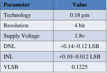
www.wjert.org 86 III. Simulation and Characterization Results of 4-BIT FL ASH ADC using 0.18µm TECH
Figure 7: Transient response of the 4-bit flash ADC for ramp signal.
Table 1: Comparision of Comparators for ±5% Power Supply Variations.
Table 2: Comparator transistor size used in 0.25µm technology. Comparator Vdd variations Minimum
Vm in volts
Maximum Vm in volts
TIQ
1.8v 0.71586 0.81448
1.71v (-5%) 0.68897 0.78759
1.89v (+5%) 0.75172 0.85034
CMOS- LTE
1.8v 0.87377 0.92899
1.71v (-5%) 0.87448 0.92828
1.89v (+5%) 0.87377 0.92756
CMOS-NAND
1.8v 0.90604 0.96127
1.71v (-5%) 0.90676 0.96199
1.89v (+5%) 0.90676 0.96342
Technology Comparator Wp (µm) Wn (µm) Vm (v) Analog input range
0.25µm Min comp
Max. comp 0.42 µm 2.72 µm 0.18 µm 1.9 µm 1.19439
2.03960 1.19 - 2.03
0.18 µm Min comp
Max. comp 0.27 µm 2.7 µm 1.35 µm 0.15 µm 0.87377
0.92899 0.87 - 0.92
0.09 µm Min comp
Max. comp 42n 1.72 µm 90n 450n 0.62760
www.wjert.org 87 Table 3: Process Variations.
Table 4: ADC Performance.
IV. CONCLUSIONS
LTE Comparator Flash ADC and CMOS-NAND Comparator Flash ADC have been designed
and simulated with 180 nm technology. The results obtained are encouraging and indicate
that the CMOS-LTE Comparator approach has the advantage of better power supply noise
rejection. Also the power dissipation is reduced because of the internally generated reference
voltages. Future NAND based topology is used which improves PSRR as well as linearity;
thus eliminates basic limitation of TIQ inverter.
REFERENCES
1. Meghana Kulkarni1, V. Sridhar2, G.H. Kulkarni3. “4-Bit Flash Analog to Digital
Converter Design using CMOS-LTE Comparator” 978-1-4244-7456-1/10/$26.00 ©2010
IEEE
2. Ali Tangel and Kyusun Choi. “The CMOS Inverter as a Comparator in ADC Design”.
Analog Integrated Circuits and Signal Processing, 2004; 39: 147-155.
3. E.Sall and M. Vesterbacka. “A multiplexer based decoder for flash analog-to-digital
converters,” Proc. TENCON, 2004, Nov. 21-24.
Process Min. Vm (V)
Max. Vm (V)
VFSR (V)
VLSB (V)
TT 1.196399 2.040600 0.844201 0.06030
SS 1.3934 1.760600 0.3672 0.02622
FF 1.305399 1.774600 0.46921 0.03351
SF 1.390399 1.801599 0.4112 0.02937
FS 1.328399 1.774600 0.446201 0.03187
Deviation 0.197 0.28 0.47 0.034
Parameter Value
Technology 0.18 µm
Resolution 4 bit
Supply Voltage 1.8v
DNL +0.14/-0.12 LSB
INL +0.10/-0.012 LSB
www.wjert.org 88
4. G.L.Madhumati, K.Ramakoteswara Rao, M.Madhavi Latha, “Comparison of 5-bit
Thermometer- to-Binary Decoders in 1.8V, 0.18μm CMOS Technology for Flash ADCs,”
Proceedings of 2009 International Conference on Signal Processing Systems (ICSPS
2009), May 15-17, 2009, Singapore, pp. 516-520.
5. Jincheol Yoo, Kyusun Choi, and Jahan Ghaznavi, “Quantum Voltage Comparator for
0.07μm CMOS Flash A/D Converters”, Proceedings of the IEEE Computer Society Annual Symposium on VLSI (ISVLSI‟03).
6. Excert from textbook “Analysis & Design of analog Integrated circuits” by Gray &
Meyer 2nd edition.
7. S.Park and R. Schaumann, “A High-Frequency CMOS Linear Trasconductansce
Element,” IEEE trans. Circuits Syst, vol. CAS-33, no.11, November, pp. 1132-1138,