DESIGN OF MTCMOS LOGIC
CIRCUITS FOR LOW POWER
APPLICATIONS
V.LeelaRani1 Dr.M.MadhaviLatha2
1. Associate professor ,Department of ECE ,Visakhapatnam, AP, India. lee_rani@gvpce.ac.in
2. Professor, Department of ECE, JNTU College of Engineering, Hyderabad, AP, India. mlmakkena@yahoo.com
Abstract
Technology scaling leads to sub threshold leakages in deep sub micron regime. There is a need for effective leakage reduction techniques to minimize MOS leakage currents. Reduced leakage currents extend the life of all battery operated devices like cell phones,Laptopsetc. This paper presents multi threshold CMOS circuit level technique to minimize leakages. MTCMOS technique is an effective solution for high-speed low-power applications. The proposed technique has been implemented in cadence virtuoso tool using standard cells of 90nm CMOS technology. For performance evaluation a full adder and 4x4 multipliers are considered as test circuits and applied with MTCMOS technique. Simulation results proved that MTCMOS technique is best in minimizing power compared with the conventional and dual threshold voltage techniques and can be used for low power applications .
Keywords – MTCMOS, DualVt, static power, dynamic power.
1.Introduction
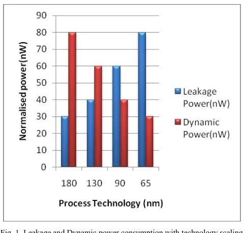
The growth of semiconductor industry driven by the advancements of the IC technology and the market dynamics was predicted by Gordon Moore in 1965[1].With the advancement in technology, static power dominates dynamic power dissipation. In current CMOS technologies sub threshold leakage current is larger than other leakage current components. As technology scales down to nanometer, sub threshold leakage power increases exponentially with the reduction of supply voltage (V DD) and the threshold voltage (V th)[2]. Sub threshold leakage is the current flowing during weak inversion mode when the transistor is in turn off state. Minimizing leakage power is an important task in portable devices to increase the battery life. Fig. 1 shows static power is comparable to dynamic power with the current trend of technology scaling.
Fig. 1. Leakage and Dynamic power consumption with technology scaling
MTCMOS technique are designed and simulation results are compared with the conventional and dual threshold voltage circuits.
This paper is organized as follows. Section II gives brief description of sources of power dissipation and Dual threshold voltage technique is given in section III. Section IV presents MTCMOS technique. Section V deals with circuit designs with MTCMOS technique and section VI presents simulation results and analysis of circuits designed. Finally, section VII concludes the paper.
2.Sources of power dissipation
Power dissipation in CMOS circuits can be categorized in to static power, dynamic power and short circuit power. Static power is the dissipation caused by CMOS circuit when it is in standby mode. Various leakage components that constitute static power are sub threshold leakage, gate oxide tunneling leakage, reverse bias leakage. Static power can be expressed as ,
P static = V DD I leakage ---(1)
Dynamic power dissipation is from current flow during logic transitions. CMOS circuits dissipate power by charging the various load capacitances whenever they are switched[8]. Dynamic power can be expressed as P dynamic = α C LV DD 2 f ---(2)
Where α is switching activity factor, C L is load capacitance, VDD is supply voltage and f is the operating frequency. MOS transistor transitions from OFF to ON or ON to OFF, both PMOS and NMOS transistors under ON state will create a short circuit path from VDD to gnd. This leads to short circuit power dissipation. Various leakage reduction approaches like MTCMOS and Dual threshold voltage techniques are discussed in later sections.
3. MTCMOS Leakage Reduction Technique
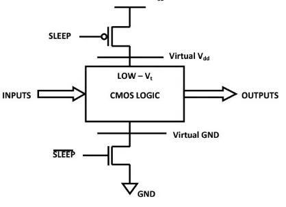
MTCMOS logic is an effective standby leakage control technique. Multi threshold logic makes use of low Vth and high Vth MOS transistors to satisfy both low power and high performance requirements. Between logic circuitry and power supply rails high Vth sleep transistors are used. These sleep transistors are enabled through sleep signals. High threshold transistors are used as sleep transistors to reduce power consumption in standby mode[3]. Low Vth transistors are used in the logic circuit to increase the performance during active mode.
Fig. 2 .MTCMOS general structure
Fig.2 shows the general MTCMOS circuit structure. High Vth PMOS and NMOS transistors connected between logic circuit and supply rails. Sleep signal activates high threshold transistors during active mode for actual logic operation. High Vth transistors are under turn off state during standby mode to cutoff logic circuit from supply rails. This minimizes the subthreshold leakages to flow during standby mode. MTCMOS can be an effective technique for low power and high speed applications. Sizing of high threshold transistors is one of the tasks to be looked in to when designing a circuit with MTCMOS structure.
4. Dual threshold voltage technique (dual-vt)
5. Circuit design with MTCMOS and Dual Vt techniques
Full adder and 4x4 multipliers are considered in this paper as test circuits and designed with MTCMOS and dual threshold voltage techniques.
5.1. Design of full adder
Full adder is one of the most critical components of a processor that determines its throughput [9]. Addition of two bits along with third bit called carryin can be performed by fulladder. Fig.3 shows conventional one bit full adder circuit. In this paper full adder logic is implemented with MTCMOS and dual threshold techniques. Above two techniques along with conventional circuit are compared in terms of static and average powers. Adder logic performs addition during active mode when sleep transistors are ON. During standby mode adder circuit is cut off from supply rails by turning off high Vth sleep transistors.
Fig. 3. Conventional One bit Full adder
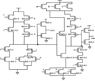
5.2.Design of 4x4 multiplier
Fig .4 General architecture of 4X4 Carry-save multiplier[11]
Table .1 Comparison results for 1-bit Full adder
Table .2 Comparison results for 4x4 Multiplier
parameter Conventional circuit Dual Vt circuit MTCMOS Circuit
Static power (w) 3.3 x 10 -8 3.27x 10 -8 2.89x 10 -8
Average power(w) 5.3x 10 -7 1.87x10 -7 1.5x 10 -7
parameter Conventional circuit Dual Vt circuit MTCMOS Circuit
Static power (w) 7.59x 10⁻⁷ 5.52x10 -7 5.38x 10⁻⁷
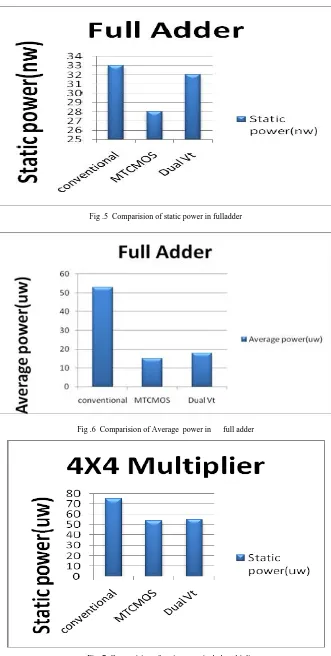
Fig .5 Comparision of static power in fulladder
Fig .6 Comparision of Average power in full adder
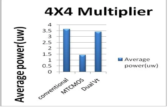
Fig .8 Comparision of Average power in 4x4 multiplier
6.Results and analysis
The proposed full adder and multiplier circuits are simulated using cadence virtuoso tool with 90nm process technology. Tables 1 & 2 shows comparision of MTCMOS, Dual Vt techniques with respect to conventional circuits for full adder and multipliers in terms of static power and average power. Table.1 and Table.2 shows that MTCMOS has reduction of static and average powers compared to conventional and dual Vt full adder and multiplier circuits. Figures 5 and 6 shows comparision charts for full adder in terms of static and average powers. Figures 7 and 8 presents comparision for 4x4 multiplier in terms of static and average powers. 7. Conclusions
This paper presents a multi threshold CMOS logic, an effective standby leakage control technique. MTCMOS technique can greatly reduce leakage power by making use of low threshold and high threshold MOS transistors. From the simulation results we can conclude that MTCMOS can achieve reduction of static and average powers compared to dual threshold voltage technique and conventional methods.
References
[1] Shaym akashe,Nitesh kumar.T,Jayaram shrivas, Rajeevsharma:A novel high speed & power efficient half adder design using MTCMOS Technique in 45 Nanometer Regime, IEEE International conference on Advanced Communication Control and Computing Technologies(ICACCCT), 2012.
[2] Phani kumar.M,N.Shanmukha Rao :A low power and high speed Design for VLSI Logic circuits using Multi-Threshold Voltage CMOS Technology : International journal of computer science and information Technologies,vol.3,2012.
[3] Milind Gautam,Shaym Akashe :Reduction of Leakage current and power in full subtractor using MTCMOS Technique , international conference on computer communication and informatics(ICCCI),Jan 2013.
[4] Paanshul Dobriyal,Karna Sharma,Manan sethi,Geetanjali sharma :A High performance D-Flipflop Design with Low power clocking system using MTCMOS technique,3rd IEEE International Advance Computing conference(IACC) ,2012.
[5] Shyam akashe,Vinod Rajak,Gunakesh,Richapandey: Estimation of high speed encoder with MTCMOS technique in 45 Nanometer Era,World congress on Information and communication Technologies, 2012.
[6] Wenxin Wang,Mohab anis,Shawki Arebi: Fast Techniques for standby Leakage Reduction inMTCMOS circuits, IEEE international conference ,2004.
[7] Harry I.A.Chen,Edward K.W.Loo,James B.Kuo,Marek J.Syrzcki: Triple Threshold static power minimization techniques in High-level synthesis for Designing high speed low power SOC applications using 90nm MTCMOS technology, IEEE international conference , 2007.
[8] Ester Rani.T,Dr.RAmeshwar Rao: Low power high performance Baud Rate generator using MTCMOS voltage Interference circuits,International journal of Engineering Research and applications (IJERA),vol.2,Issue 4,pp.1621-1626,aug 2012.
[9] Ester Rani.T,Dr.Rameshwar Rao: Area and power optimized multipliers with minimum leakage,IEEE 3rd International conference on Electronics computer technology (ICECT 2011).
[10] Jun cheol park,Vincent Mooney: Sleepy stack leakage reduction,IEEE transactions on VLSI systems,vol.14,no.11,Nov 2006. [11] Sailaja.K,Leelarani.V,Akram.SK: Analysis of Leakage power reduction techniques for low power VLSI design, International journal
of computer applications,vol-82, Nov 2013.
[12] Jaffari.J and Afzali-Kusha:New Dual-Threshold Voltage Assignment Technique for Low-Power Digital Circuits, 0-7803-8656-6/04/$20.00, pp.413-416 IEEE 2004.
![Fig .4 General architecture of 4X4 Carry-save multiplier[11]](https://thumb-us.123doks.com/thumbv2/123dok_us/9667881.1494683/4.595.143.443.69.271/fig-general-architecture-x-carry-save-multiplier.webp)