International Journal of Research in Engineering and Applied Sciences(IJREAS) Available online at http://euroasiapub.org/journals.php
Vol. 7 Issue 5, May-2017, pp. 37~45
ISSN (O): 2249-3905, ISSN(P): 2349-6525 | Impact Factor: 7.196 | Thomson Reuters Researcher ID: L-5236-2015
A High Competence Class AB CMOS Power Amplifier for Wireless Applications
RENUKAPRASAD.G1,
Assistant prof.EEE Department
Dayananda Sagar Academy of Technology and Management (DSATM) Kanakapura Road , Bangalore, India.
E-Mail: renukaprasad25@gmail.com
Shashikiran B S2,
Assistant Professor, ECE Department VKIT, Bangalore,India
Santosh M Nejakar3
Assistant Professor, ECE Department DBIT,Bangalore, India
Abstract
A power amplifier is an amplifier designed primarily to increase the power available to a load. In practice, amplifier power gain depends on the source and load impedances, as well as the inherent voltage and current gain. A radio frequency (RF) amplifier design typically optimizes impedances for power transfer, while audio and instrumentation amplifier designs normally optimize input and output impedance for least loading and highest signal integrity. In this paper projected a new method for maximizing the power added efficiency was presented. A 3.0-7.0 GHz class AB CMOS PA with CG driver stage followed by CS power stage was designed using the proposed method for WBAN applications
Keywords: Power Amplifier (PA), Radio Frequency(RF), Wireless Body Area Network(WBAN),
1. INTRODUCTION
International Journal of Research in Engineering and Applied Sciences(IJREAS) Vol. 7 Issue 5, May-2017
ISSN (O): 2249-3905, ISSN(P): 2349-6525 | Impact Factor: 7.196
compression at rated output), input and output impedance matching, and heat dissipation.
Fig.1.1. Functional block diagram of PA
Figure.1 shows the basic functional block diagram of PA. The input signal to the amplifier from the source will be generally in the mill volt range. One of the most important design methods for PA still consists of matching the large signal input and load impedance of an active device.
The output power efficiency is associated with that large signal impedance. Nevertheless, these parameters not only depend on the large signal impedance but also on matching networks. The purpose of the driver (PA) stage is to produce enough amplification and current gain in order to drive the output stage. Since there is sufficient current gain, the stage produces considerable amount of power gain too.
Output stage is the stage that is connected to the loudspeaker. The output stage gives further improvement to the power gain and transfers this power to the loudspeaker with minimum loss.For class A PAs, the transistor is performing for half the RF cycle, whereas for class B PAs it is active for half the RF cycle, and for less than half the RF cycle for class C PA. Class A, AB, and B amplifiers may be used as linear PAs, whereas class C is more nonlinear in attributes.
The class AB amplifier is biased above its turn-on voltage and the input propels the device on for a small fragment, which is slighter than half of the input cycle. This results into a pulsed current in the device. The efficiency of class-AB power amplifier diversifies from 60% to 90%.A Class-AB PA is a sole variety of an amplifier where the transistor conducts between 180° to 360°. The operating point of the transistor is hooked in the cut off region. The dc section of the gate-to-source voltage VGS which is beneath the transistor threshold voltage Vt. On this ground, the conduction
angle of the drain current is between 180° and 360°.
The power output of an amplifier is the product of the voltage and current, (P = V*I) applied to the load, while the power input is the product of the DC voltage and current taken from the power supply.
Although the amplification of a Class A amplifier, (where the output transistor conducts 100% of the time) can be high, the efficiency of the conversion from the DC power supply to an AC power output is generally poor at less than 50%. However if we modify the Class A amplifier circuit to operate inClass B mode, (where each transistor conducts for only 50% of the time) the collector current flows in each transistor for only 180o of the cycle. The advantage here is that the DC-to-AC
conversion efficiency is much higher at about 75%, but this Class B configuration results in distortion of the output signal which can be unacceptable.
International Journal of Research in Engineering and Applied Sciences(IJREAS) Vol. 7 Issue 5, May-2017
ISSN (O): 2249-3905, ISSN(P): 2349-6525 | Impact Factor: 7.196
[1] H.-C. Chen, M.-Y.Yen, Q.-X.Wu, K.-J.Chang, and L.-M. Wang, “Battery less Transceiver Prototype for Medical Implant in 0.18-m CMOS Technology,” IEEE Trans. Microw. Theory Tech., vol. 62, no. 1, pp. 137–147, Jan. 2014.
This paper presents a medical implant communication service/industrial-scientific-medical band battery less transceiver prototype for medical implants is proposed and implemented using 0.18-μm CMOS technology. An RF-dc converter is used to accomplish the battery less function of the transceiver, where the RF powering source is also the reference signal source for the frequency synthesizer. MOS-bipolar devices are employed in receiver analog band circuits as pseudo-resistors. Dissipating 2.19mW in the receive mode, the transceiver achieves a sensitivity from -68 to -73dBm for a BER <; 10-3, at a data rate of 20 kb/s.
[2] “IEEE Standard for Local and Metropolitan Area Networks - Part 15.6: Wireless Body Area Networks.”pp. 1–271, 2012.
Short-range, wireless communications in the vicinity of, or inside, a human body (but not limited to humans) are specified in this standard. It uses existing industrial scientific medical (ISM) bands as well as frequency bands approved by national medical and/or regulatory authorities. Support for quality of service (QoS), extremely low power, anddata rates up to 10 Mbps isrequired while simultaneously complying with strict non-interference guidelines where needed.
[3] R. Sapawi, R. K. Pokharel, D. A. A. Mat, H. Kanaya, and K. Yoshida, “A 3.1–6.0 GHz CMOS UWB Power Amplifier with Good Linearity and Group Delay Variation.”pp. 9–12, 2011. This paper presents a design of 3.1-6.0 GHz power amplifier (PA) 0.18μm CMOS technology for ultra-wideband (UWB) applications. The UWB PA employs two stages amplifier and inter-stage circuit to provide a wider gain and gain flatness while shunt resistive feedback technique is adopted at the input stage to provide wideband input matching. To obtain high and flat gain, good group delay variation and linearity at the same time, the inductive peaking technique and Class A PA are employed at the first stage and the second stage.
[4] V. P. Bhale, A. D. Shah, and U. D. Dalal, “3–5 GHz CMOS Power Amplifier Design for Ultra-Wide-Band Application,” in 2014 International Conference on Electronics and Communication Systems (ICECS), 2014, pp. 1–4.
This paper presents the design of a wideband class AB cascode Power Amplifier (PA) using UMC 0.18μm CMOS process for UWB applications covering lower band of 3-5 GHz. Designed class AB PA delivers an output power of 1.80267 dBm at an input 1-dB compression point of -11.144 dBm for a 4 GHz frequency. It achieves a good gain flatness of 13.3±1.0 dB over the entire 3-5 GHz. The matching networks are designed to achieve an input and output return loss of <;-7.5 and <;-7.0 dB respectively, with an excellent reverse isolation of <;-37 dB. Power Added Efficiency (PAE) is found to be 15.32% at -5 dBm input RF power. The designed PA also found to be un-conditionally stable.
PROBLEM FORMULATION
International Journal of Research in Engineering and Applied Sciences(IJREAS) Vol. 7 Issue 5, May-2017
ISSN (O): 2249-3905, ISSN(P): 2349-6525 | Impact Factor: 7.196
Body Communications (HBC) layers. The UWB PHY supports the frequency range from 3494.4 MHz to 9984 MHz; this range is divided into 11 channels three in low band (channels 0-2) and eight in the high band (channels 3–10) with 499.2 MHz bandwidth for each channel [4]. Many UWB designs were presented in literature in CMOS technology for the frequency ranges 3-5 GHz, 3.1-6 GHz, 3-7.5 GHz and 6-10.6 GHz. Power added efficiency is an important metric in the UWB-PA design as it measure how effectively the DC power is converted to RF output power. In addition, group delay is very important as it is measure of phase nonlinearity.
2. PROPOSED METHODOLOGY
The author has proposed a methodology in which a high efficiency CMOS power amplifier operating from 3 GHz to 7 GHz with a minimum group delay variations for a WBAN transmitter is designed and simulated using 0.18 um CMOS process.
CIRCUIT DESCRIPTION
Fig.2.1. Schematic of the proposed PA
The proposed two stages wideband PA consists of common gate (CG) driver stage followed by common source (CS) power stage as shown in Figure 2.1. The CG driver stage is composed of transistor M1 loaded by diode connected transistor M2.. The second stage composed of a CS amplifier M3 biased in class AB to enhance the PAE which is important to deliver desired power for WBAN transmitter. Figure 2.2shows the drain I-V wave forms at 5 GHz indicating class AB operation. Resistor RBIAS is used to adjust the biasing for transistor M3. The inductors L3 and L4
form a shunt and series peaking to provide wideband output impedance matching, flat gain, small group delay variation and maximum power added efficiency.
International Journal of Research in Engineering and Applied Sciences(IJREAS) Vol. 7 Issue 5, May-2017
ISSN (O): 2249-3905, ISSN(P): 2349-6525 | Impact Factor: 7.196
Fig.2.3. Small signal equivalent circuit of the proposed PA,
POWER ADDED EFFICIENCY ANALYSIS
Figure 2.3 shows the small signal equivalent circuit of the proposed Wideband PA. The output impedance of the first stage Zout1 is the source impedance seen by the power stage and canbe expressed by Eq.1.
𝑍𝑜𝑢𝑡1 =𝑆2𝐿2𝐶𝑒𝑞𝑔𝑚2+𝑆𝐶𝑒𝑞+𝑔𝑚2
𝑆𝐶𝑒𝑞𝑔𝑚2 (1)
Where𝐶
𝑒𝑞=𝐶1𝐶𝑔𝑠3 𝐶1+𝐶𝑔𝑠3
gm = transconductance of the
MOSFET
In order to maximize the power added efficiency of the proposed UWB-PA, source and load-pull simulation template in Agilent Advanced Design System (ADS) is employed to determine the optimal conditions for maximum PAE of the proposed UWB-PA. Using source-pull simulation, the input power was fixed at -5 dBm while the source impedance was being varied and the load impedance was fixed at 50 ohms. Figure 2.4 shows the constant PAE contours at 3 GHz, 5 GHz and 7 GHz for different source impedances for the second stage UWB-PA. The inter-stage matching is designed using inductor L2 in order to make the output impedance of the first stage following the source-pull contours of second stage. The load-pull simulation is employed for the two stages PA in order to get optimal load to maximize the PAE. Figure 2.5 shows the constant PAE contours at 3, 5 and 7 GHz for different load impedances for the proposed UWB-PA.
The output impedance of the two stages PA can be expressed by Eq.2:
𝑍𝑜𝑢𝑡 =𝑆𝐿3[𝑆2𝐿4𝐶𝑜𝑢𝑡+1] 𝑆2𝐶
𝑜𝑢𝑡[𝐿3+𝐿4]+1 (2)
Fig.2.4. Constant PAE contours in 4% step using source-pull
International Journal of Research in Engineering and Applied Sciences(IJREAS) Vol. 7 Issue 5, May-2017
ISSN (O): 2249-3905, ISSN(P): 2349-6525 | Impact Factor: 7.196
impedances for the second stage UWB-PA.
Fig.2.5. Constant PAE contours in 4% step using load-pull
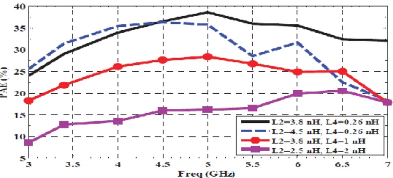
Figure 2.6 shows the effect of varying L2 and L4 on the PAE. L2 also largely affect the gain flatness. The output matching circuit is designed using the inductor L4 in order to make the output impedance Zout follow the load pull contours at figure 2.5. From the above analysis, L2 and L4
have major role in maximizing the PAE. Therefore, Figure 2.6 shows the effect of varying L2 and
L4 on the PAE. L2 also largely affect the gain flatness. Figure 3.3 shows the effect of varying L2 on gain flatness. Therefore, to maximize PAE and achieve reasonable gain flatness using figure 2.6 and figure 3.3, the values of L2 and L4 are optimized to be 3.8nH and 0.26nH.
Fig.2.6. Effect of L2 and L1 on power added efficiency.
3. SIMULATION RESULTS
Figure 3.1 shows the layout of the proposed UWB-PA using Cadence virtuoso layout editor in TSMC CMOS 0.18um process. The die area of the proposed PA occupies 0.78 mm2 including
measurement pads. Figure 3.2 shows the similarities between post and pre-layout S-parameters results using Cadence Spectre RF simulator. As shown in figure 3.2 the input return loss S11 and the output return loss S22 are less than -10 dB and -11 dB respectively over the frequency range of interest. This is done by successfully designing the input and output matching circuits. This broadband input and output impedance matching enhance the PAE further.
Power-added efficiency (PAE) is a metric for rating the efficiency of a power amplifier that takes into account the effect of the gain of the amplifier. It is calculated (in percent) as: In addition, the proposed PA achieved an average gain S21 of 12 dB with gain flatness of ±0.8 from 3 to 7 GHz. This PA can be used from 2 GHz to 8 GHz with power gain of 11.7 dB ± 1, input and output return losses are less than -5 dB and -7 dB respectively.
International Journal of Research in Engineering and Applied Sciences(IJREAS) Vol. 7 Issue 5, May-2017
ISSN (O): 2249-3905, ISSN(P): 2349-6525 | Impact Factor: 7.196
7 GHz respectively which is the result of the PAE analysis discussed in section III.
The proposed UWB-PA achieved 1-dB compression points of 10.5, 7.21 and -1dBm at 3, 5 and 7 GHz respectively as shown in Figure 3.6. Finally, the proposed PA is unconditionally stable over the frequency band from 1 GHz to 10 GHz. The PA operated from 1.8 V supply and consumed about 32mW.Table I shows aperformance summary of the proposed PA in comparison to recently published 0.18um CMOS UWB-PAs.
Fig.3.1. Layout of proposed PA (0.97 mm * 0.78 mm)
Fig.3.2 Post-Layout Simulation of S-Parameters
Fig.3.3. Effect of L2 on gain flatness
International Journal of Research in Engineering and Applied Sciences(IJREAS) Vol. 7 Issue 5, May-2017
ISSN (O): 2249-3905, ISSN(P): 2349-6525 | Impact Factor: 7.196
Fig.3.5. Post-Layout Simulation of 1-db compression point
4. CONCLUSION
Here the author proposed a new method for maximizing the power added efficiency was presented. A 3.0-7.0 GHz class AB CMOS PA with CG driver stage followed by CS power stage was designed using the proposed method for WBAN applications. The post layout simulation results showed that the proposed PA has an average gain of 12±0.8 dB also input and output impedance matching less than -10 dB over the frequency of interest. In addition, The PA achieved maximum PAE of 38.5% at 5 GHz and good output compression characteristics beside good phase linearity.
REFERENCES
[1] H.-C. Chen, M.-Y. Yen, Q.-X. Wu, K.-J. Chang, and L.-M. Wang, “Batteryless Transceiver Prototype for Medical Implant in 0.18-m CMOS Technology,” IEEE Trans. Microw. Theory Tech., vol. 62, no. 1, pp. 137–147, Jan. 2014.
[2] Federal Communication Commission “Revision Of Part 15 Of The Commission's Rules Regarding Ultra-Wideband Transmission Systems,” First Report and Order, ET Docket 98-153, FCC 02-48, April 2002.
[3] “IEEE Standard for Local and Metropolitan Area Networks - Part 15.6: Wireless Body Area Networks.” pp. 1–271, 2012.
[4] [4] Sana Ullah, ManarMohaisen, and Mohammed A. Alnuem, “A Review of IEEE 802.15.6 MAC, PHY, and Security Specifications,” International Journal of Distributed
Sensor Networks, vol. 2013, Article ID 950704, 12 pages, 2013.
[5] V. P. Bhale, A. D. Shah, and U. D. Dalal, “3–5 GHz CMOS Power Amplifier Design for Ultra-Wide-Band Application,” in 2014 International Conference on Electronics and Communication Systems (ICECS), 2014, pp. 1–4.
[7] R. Sapawi, R. K. Pokharel, D. A. A. Mat, H. Kanaya, and K. Yoshida, “A 3.1–6.0 GHz CMOS UWB Power Amplifier with Good Linearity and Group Delay Variation.” pp. 9–12, 2011.
[8] S. A. Z. Murad, R. K. Pokharel, H. Kanaya, K. Yoshida, and S. A. . Murad, “A 3.0–7.5 GHz CMOS UWB PA for group 1~3 MB-OFDM Application Using Current-Reused and Shunt-Shunt Feedback,” in 2009 International Conference on Wireless Communications & Signal Processing, 2009, pp. 1–4.
International Journal of Research in Engineering and Applied Sciences(IJREAS) Vol. 7 Issue 5, May-2017
ISSN (O): 2249-3905, ISSN(P): 2349-6525 | Impact Factor: 7.196
Biography of Authors
RENUKAPRASAD.G
I have done B.E (Electrical & Electronics) from UBDTCE, Davangere , M.Tech(CAID) from MCE, Hassan. I worked at ADA - Bangalore. I am currently working in Dayananda Sagar Academy of Technology and Management , Bangalore from last Five Years as Assistant Professor in Electrical and Electronic Engineering Department. My Area of interest is towards Drives(Machines) , Power electronics, Renewable energy resources.
Shashikiran B S
I have done B.E (E&C) from UBDTCE, Davangere , M.Tech(Biomedical Signal processing) from RVCE, Bangalore. I am currently working in Vivekananda Institute of Technology, Bangalore from last Six Years as Assistant Professor in Electronics and Communication Engineering Department. My Area of interest is towards Digital Signal Processing , Image Processing and Embedded Systems.
Santosh M Nejakar