An Image Based Pad Parameters Measurement Method for Printed Circuit Board
Bangshu Xiong, Yanan Zhang, Lei Yu, Chengli Sun
Key Laboratory of Nondestructive Test of Ministry of Education Nanchang Hangkong University
Nanchang, 330063, China.
ABSTRACT: An accurate pad parameters measurement method for printed circuit board (PCB) is proposed in this paper. Firstly, the measured pad is selected by drawing a circle around it, then the processing image is de-noised and segmentation. After that, the teardrop in connected area of the pad and line is excluded. Secondly, all the possible edge points around the pad are detected by Sobel operator and Zernike moment is used for localization of the edge points on a sub-pixel level. Finally, the detected circle edge of the pad is fitted by a least-square algorithm and the pad diameter and center position are derived. Experimental results reveal that the proposed method is precise, quick and stable, and it has already been applied in our self-developed “automatic optical measurement instrument (AOM1.1)”system.
Keywords: Printed Circuit Board, Parameters Measurement, Sobel Operator, Sub-pixel Location, Camera Linear Calibration
Received: 15 May 2015, Revised 20 July 2015, Accepted 28 July 2015
© 2015 DLINE. All Rights Reserved 1. Introduction
With the development of electronic technique, electronic products are growing popularly. Printed circuit boards (PCB) has been widely used in the modern electronics industry. Current miniature integrated circuit (IC) puts forward higher requirements to the production of PCB, such as intensive line width and multiple layer board design. Generally, a multilayer PCB consists of several single-layer PCBs. Even one slight mistake of each layer of PCB will result in the failure of the whole board. Therefore, the accurate pad parameters measurement is a very important step for PCB productions design. In the past, pad parameters were usally measured by the means of hundredfold mirror and common second element techniques. However, the hundredfold mirror method depends on the experience of experts and has low efficiency. With respect to the common second element method, it is hardly worked due to the inconvenient operation.
Image measurement based on the machine vision[1]is a new measurement technology developed in recent years. This new technology has the characteristics of high precision and lossless, which has been widely used in various fields such as indus-try[2], agriculture[3], medicineand others[4]. So far, the literature about PCB pad measurement is relatively few and most of them are
on a pixel level. In this article, we introduce a new approach for measuring the parameters of pad based on image measurement technology, and develop the PCB measuring system, which is highly efficient and accurate.
2. Structure of the Hardware System
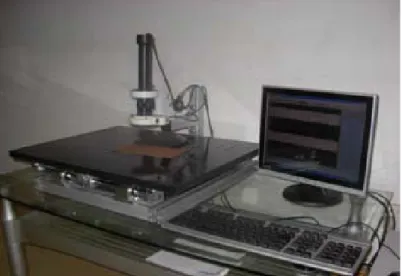
illumination device, image acquisition card and PC computer. It is shown in Fig.1. In this system, the resolution ratio of the standard video camera is 768*576, the lens magnification rate is 40X to 220X, and the video capture card’ model is OK-C20A. When measuring pad parameters, the PCB is fixed to the movable platform firstly. Then the lighting device is adjusted carefully, so that light spread onto the test area evenly. After this step, the colorful PCB to be measured is projected to CCD. Finally, video capture card converts the analog signal into digital video and shows it on computer screen.
Figure 1. The self-developed “Automatic optical measuring instrument (AOM1.1)” system
3. Description of Measuring Method
The main steps of the measurement method can be summarized as follows: (1) Image preprocessing for image denoising. (2) Removing teardrop around the pad. (3) Detecting pad edge and removing abnormal points. (4) Locating the edge points on the sub-pixel level and fitting the circle around the pad. (5) Calibrating the system and calculating the actual parameters of the pad. 3.1 Image Preprocessing
Image preprocessing is an important step to improve the accuracy of measurement. Firstly, the measurement area is selected by drawing a circle around the pad, as shown in Fig.2. After that, two steps are followed: image denoising and segmentation. In this article, we choose the median filter for eliminating noise, the reason is that median filter can preserve the edge information well when remove noise. We transform the corlorful measuring image into a gray image by gray-scale transformation. And then Otsu[5]
lagorithm is applied to separate the foreground from background with a threshold t*. 3.2 Remove the Teardrop around the Pad
To improve the stability of welding circuit, teardrop is often added into the connected region of pad and line within a PCB. In practice, the teardrops must be removed before measuring pad, as it will affect the pad fitting accuracy. In this work, we dislodge teardrops based on the principle that the brightness of background is less than that of the pad. The details are depicted as following steps:
Step 1: First, we choose a point on the circle as starting point. If the brightness of the start point is greater than t*, it indicates the
point will be on the connected area, and goto step2; otherwise, goto step3.
Step 2: Starting from the initial point, we scan the circle with every1o in clockwise and counterclockwise direction respectively. In
this way, the two connection points A and B will be obtained, as shown in Figure.2, and goto step4.
Step 3: In this step, we scan the circle from the starting point at the same interval of angle in the clockwise direction. If the brightness value of scanning point is greater than t*, a connection point will be found and denoted as A. And then, another point B will be found in the same way.
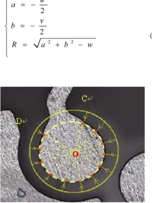
Step 4: According to the characteristic of tears, points A and B are moved to C and D at an angle. In this work, the angle is 25o.
Figure 2. The sketch map of teardrop area 3.3 Edge Detection
In this section, Sobel operator is used to detect the pad edge points, as is shown in Figure.3. Sobel operator is known to be insensitive to noise and it has relatively small mask than other algorithms[6]. The details about Sobel operator can be seen in [9].
Then, we search the edge point set based on scanning in the polar coordinate. And the main process is as follows:
Firstly, Starting from point D, we taking a point every 5o on the circle and searching to the direction of point O. If the pixel value of the point is 255, it will be the edge point. As the red points shown in Figure. 4. In the same way, all the edge points will be searched.
Secondly, Least squares circle fitting method (see subsection 3.4) is used to obtain the center coordinates of the pad circle. The process is depicted in Figure.5.
Finally, The distance from each edge point to the center is calculated and they are sorted in descending order. The first third of the distance and the last third of the distance will be removed as the abnormal points.
Figure 3. The result of pad edge detection
3.4 The Principle of Least Squares Fitting Method
Let the center coordinate be (a, b), radius is R, and the equation of a circle is: (x −a)2 + (y −b)2 = R2 (1)
The basic principle of least squares circle fitting is to find a circle so that the square sum of error F between edge points set (xi
−yi) (i = 1, 2, ... n ) is minimized[7].
(2)
To facilitate the computation, we convert formula (2) is to formula (3).
(3)
where . The parameters u, v, w can be calculated under the extreme conditions of multivariate functions. And the parameters a, b, R of the fitting circle can be obtained according the following formula.
(4)
Figure 5. The demonstration diagram of edge circle fitting
3.5 Sub-pixel Localization Based On Zernike Moment
To enhance measurement precision, we convert the original edge points into sub-pixel points by means of Zernike moment operator[8~9]
,
which can locate the edge points with sub-pixel accuracy. The detail formula can be written as:(5)
we set N to 7. L is the distance from the center to the edge. are the abscissa and ordinate of the edge points on sub-pixel level. Here, are the horizontal and vertical axis respectively. Anm is the Zernike moment of a point, A’nm is the Zernike rotational moment, is the angle between the x-axis and the vertical, which is from the center to edge. Im[A11] Re[A11] are the imaginary part and real part of A11.
3.6 System Calibration and Pad Parameters Measurement
After previous steps, we will obtain the precise edge points around the pad. To get the edge circle of the pad, we fit the sub-pixel edge points using the well-known least square fitting method. Then, the standard optical scale[10]is used to calibrate the system. Next, we determine the proportion between the pad image and actual pad target by the following formula.
where L is a known length of the standard optical scale,Nis the number of pixels in the image corresponding to L, and the unit of neighbor pixels is in mm level. Experiments show that the actual length of the object to be measured and the corresponding pixels satisfy the following linear relationship:
L = kN + b (7)
where b is systematic error in the process of measurement. k and b can be determined by calibrating the system twice, thereby eliminate the systematic error.
The parameters of the circle around the pad can be calculated by formula (4) first, then we substitute them into the formula (7) to get the actual center and the diameter (unit: mm) of a pad.
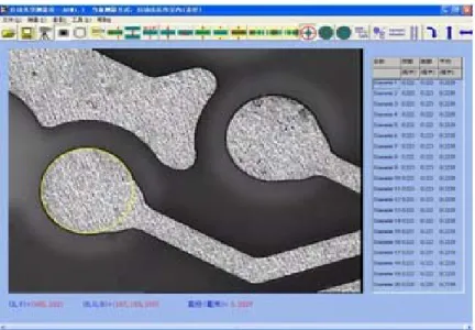
Figure 6. The interface of measuring system
4. Experiments and Results Analysis
4.1 Measurement Experiment
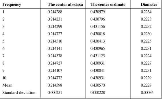
In order to verify the effectiveness and stability of the above method, Visual Studio2005 is applied to implement the measurement method. This method has been equipped into the “automatic optical measuring instrument AOM1.1” software system. The system interface is shown in Figure.6. When the use of AOM1.1 system, puts PCB on the two-dimensional movable platform first, and then set the camera magnification, adjust the camera focal length to get a clear video image of the PCB, and capture the image for measuring. The measurement results of a pad (the pad is shown in Fig.5 ) are listed in table 1. The average run-time of
the proposed method is 0.104s. As shown in table 1, the standard deviation of pad parameter is relatively small after 10 time measurements; it demonstrates that the measurement system has high accuracy and good stabilit.
Frequency The center abscissa The center ordinate Diameter
1 0.214288 0.430579 0.2234
2 0.214231 0.430796 0.2223
3 0.214299 0.431156 0.2232
4 0.214727 0.430818 0.2230
5 0.214310 0.430413 0.2225
6 0.214141 0.430965 0.2231
7 0.214378 0.431123 0.2224
8 0.214727 0.430931 0.2227
9 0.214107 0.430841 0.2231
10 0.214772 0.430931 0.2229
Mean 0.214398 0.430570 0.2228
Standard deviation 0.000251 0.000228 0.00036
Table 1. Measurement result unit: mm
4.2 Error Analysis
The measurement error of this system is mainly produced by the geometric distortion of the imaging system, image noise and imprecise location to the edge of the pad. Distortion of the imaging system is a typical system error, caused by a lens aberration, CCD pixel errors, and perspective errors.
In this work, optical lens with low distortion is used in the system to reduce the error caused by the imaging distortion. In addition, we calibrate the system with standard optical scale, it is not only unnecessary to calculate the internal and external parameters of the camera, but also can offset most of the errors from imaging aberration. The measurement results obtained under V36 lens with 4.5 X optical zoom. The system is calibrated twice with formula (7) and figure out that k = 0. 00112676, b = 0. 00112696[12].
5. Conclusions
This paper presents a method based on image for measuring the pad parameters of PCB. In this method, the median filter is used to remove image noise, least square fitting is used to remove the abnormal points of the pad and scanning method used to remove the teardrop. In the end, in order to improve the measurement accuracy of the pad parameters, we locate the point set to the sub-pixel level. The test results reveal that the method has high-accuracy and stability. Moreover, the proposed method is easy to operate and the pad measurement system has been used in the real-world PCB industrial production.
6. Acknowledgments
This research subject acquired subsidizes from Industry Support Program of Jiangxi province (item number: 2010GB00405), the Aviation Science Fund (item number: 20135756010) and Science and Technology Ground Project in College of Jiangxi province (KJLD13058).
References
[2] Hwang, B.W. (2011). Digital watermarking algorithm based on the complexity of the image texture. Computer Engineer, 37 (17), 102-104.
[3] Dworkin, S B, Nye, T J. (2006). Image processing for vision measurement of hot formed parts. Journal of Materials Processing Technology, 174 (1), 1-6.
[4] Miller, L. M, Dumas, P. (2006). Chemical imaging of biological tissue with synchrotron infrared light. Biochimica et Biophysica Acta (BBA)-Biomembranes, 1758 (7), 846-857.
[5] Carter, R. M, Yan, Y, Cameron, S. D. (2005). On-line measurement of particle size distribution and mass flow rate of particles in a pneumatic suspension using combined imaging and electrostatic sensors. Flow measurement and instrumentation, 16 (5), 309-314.
[6] Cai, L, Y. Y., Liu, Y. A. (2012). Non-embedded DCT-based watermarking using edge detection technology for Authentication. Journal of Hunan University, 39 (1), 87-92.
[7] Rosin, P. L. (1993). Ellipse fitting by accumulating five-point fits. Pattern Recognition Letters, 14 (8) 661-669.
[8] Fuchs, F., Hugger, S., Kinzer, M., et al. (2010). Imaging standoff detection of explosives using widely tunable midinfrared quantum cascade lasers. Optical Engineering, 49 (11) 111127-111127-8.
[9] QU, Y., CUI, C., CHEN, S., et al. (2003). A fast subpixel edge detection method using Sobel–Zernike moments operator. Opto-electronic Engineering, 5: 017.
[10] Vilkner, T., Janasek, D., Manz , A. (2004). Micro total analysis systems. Recent developments. Analytical chemistry, 76 (12) 3373- 3386.
[11] Zhang, G., Wei , Z. (2002). A novel calibration approach to structured light 3D vision inspection. Optics & Laser Technology, , 34 (5), 373-380.
[12] Hou, B., Y.H., Jiao, L. (2010). Improvement of SAR image by Shearlet waters edge detection. Journal of China Image, 15 (10) 1549-1554.
[13] Ghosal, S., Mehrotra, R. (1993). Orthogonal moment operators for subpixel edge detection. Pattern Recognition, 26 (2) 295-306.
[14] Hammerschlag, R. H., Skomorovskyb, V. I, Bettonvila, F. C. M, et al.(2010). The Irkutsk Barium filter for narrow-band wide-field high-resolution solar images at the Dutch Open Telescope[C]// In: Proceedings SPIE. , 7735: 773585
[15] Otsu, N. (1975). A threshold selection method from gray-level histograms. Automatica, 11 (285-296), 23- 27.
[16] Gander, W., Golub, G. H., Strebel, R. (1994). Least-squares fitting of circles and ellipses. BIT Numerical Mathematics, 34 (4), 558-578.
[17] Porco, C. C., Baker, E., Barbara, J., et al. (2005). Cassini imaging science: Initial results on Saturn’s rings and small satellites. Science, 307 (5713), 1226-1236.
[18] Nie, S. M., Tang, J. L., Guo, B. F., et al. (2005). Research on the heavy forgings dimensional metrology based on the CCD. Suxing Gongcheng Xuebao(Journal of Plasticity Engineering), 12. 85-88.
[19] Nie, S .M., Zhang, Q., Li, S. K., et al. (2006). The research of the mathematical model in the CCD measuring about the dimension of large-size forging workpiece. Journal of Plasticity Engineering, 13 (6), 110-113.
[20] Rech, R., Muller, N., Lamm, R., et al. (2006). Laser measurements on large open die forgings. Stahlund Essen, 126 (2), 53-57 [21] Takano, C., Ohta, Y. (2007). Heart rate measurement based on a time- lapse image. Medical Engineering & Physics, 29 (8), 853- 857.
[22] Zhao, Y., Wang, M., Ma, P, et al. (2006). Structured light 3D measurement technology of hot forging. China Mechanical Engineering, 17. 125-128.