R E S E A R C H A R T I C L E
Open Access
On-chip cavity optomechanical coupling
Bradley D Hauer, Paul H Kim, Callum Doolin, Allison JR MacDonald, Hugh Ramp and John P Davis
**Correspondence: [email protected]
Department of Physics, University of Alberta, T6G 2E1 Edmonton, AB, Canada
Abstract
Background: On-chip cavity optomechanics, in which strong co-localization of light and mechanical motion is engineered, relies on efficient coupling of light both into and out of the on-chip optical resonator. Here we detail our particular style of tapered and dimpled optical fibers, pioneered by the Painter group at Caltech, which are a versatile and reliable solution to efficient on-chip coupling. A brief overview of tapered, single mode fibers is presented, in which the single mode cutoff diameter is highlighted. Methods: The apparatus used to create a dimpled tapered fiber is described, followed by a comprehensive account of the procedure by which a dimpled tapered fiber is produced and mounted in our system. The custom-built optical access vacuum chambers in which our on-chip optomechanical measurements are performed are then discussed. Finally, the process by which our optomechanical devices are fabricated and the method by which we explore their optical and mechanical properties is explained. Results: Using this method of on-chip optomechanical coupling, angular and displacement noise floors of 4 nrad/√Hz and 2 fm/√Hz have been demonstrated, corresponding to torque and force sensitivities of 4×10⁻²⁰N·m/√Hz and 132 aN/√Hz, respectively.
Conclusion: The methods and results of our on-chip optomechanical coupling system are summarized. It is our expectation that this manuscript will enable the novice to develop advanced optomechanical experiments.
Keywords: Cavity optomechanics; Nanoscale transduction; Dimpled fiber; Tapered fiber; Nanomechanics
PACS codes: 07.60.-j; 07.10.Cm; 42.50.Wk
Background
State-of-the-art nanofabrication technologies have allowed for a drastic reduction in the size, and increase in quality, of nanomechanical systems, which have been the driving force behind radically increasing the sensitivity of numerous devices. Examples include accelerometers [1], mass sensors [2-6], electrometers [7], temperature sensors [8,9], force transducers [10,11] and biosensors [12-15]. The mass of a sensor and its ability to precisely measure physical quantities are intimately related, with smaller devices having superior sensitivity [5,6,11]. However, as we continue to reduce device volume, it is difficult to find transduction methods that scale appropriately. Furthermore, it is generally the case that the target quantity is measured through the nanomechanical device’s motion, hence as we move to more sensitive devices, we require a detection method with comparable
precision. A solution to these issues has been found in the field of cavity optomechan-ics, which allows for quantum-limited, sub-am/√Hz displacement sensitivity [16,17] and device masses down to the pico/femto-gram range [18-20].
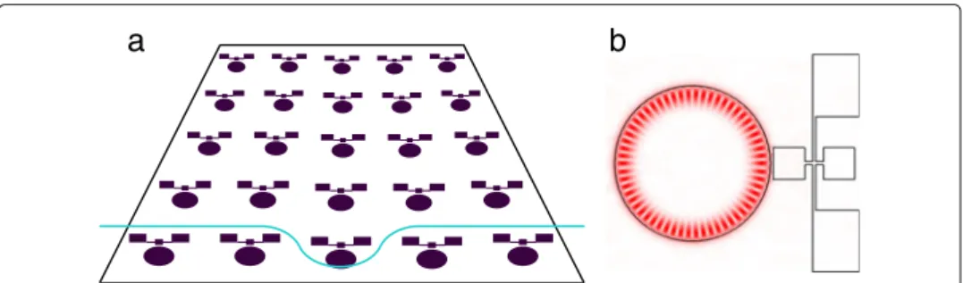
Optomechanics describes the coupling of the mechanical motion of a device to an optical field, often to manipulate or detect its motion. It is advantageous to use an opti-cal cavity, such as a whispering gallery mode (WGM) resonator [21] (see Figure 1b), to provide this field, as the light in the optical cavity is able to sample the mechanics many times due to its long photon lifetime and leads to resonantly enhanced optomechanical coupling. In such a system, the motion of the mechanical device shifts the resonance fre-quency and phase of the optical cavity. By detecting this signal, it is possible to infer the motion of the device. At the same time, photons inside the cavity apply a radiation pres-sure to the mechanical resonator [22], which can be used to optomechanically dampen or amplify its motion, leading to a large number of interesting phenomena [23]. Cavity optomechanical systems have been realized in a number of different geometries, includ-ing photonic crystal cavities [20], Fabry-Pérot etalons [24,25], WGM resonators [21,26,27] and electronic microwave cavities [28].
It is advantageous to fabricate cavity optomechanical devices on-chip, as it is therefore possible engineer both the optical and mechanical resonators to certain desired specifi-cations. Modern nanofabrication technologies make it possible to produce devices with extremely accurate dimensions, allowing feature sizes as small as 100 nm for foundry-based deep ultraviolet (DUV) optical lithography [29] and 2 nm with electron beam lithography [30]. This enables precise tailoring of important device parameters, such as the gap between mechanical and optical resonators, which controls the optomechanical coupling in our devices [21]. Furthermore, devices fabricated using top-down lithogra-phy can be integrated into electronic on-chip devices [31] and, in the case of optical lithography, can easily be mass produced.
However, difficulties arise when trying to couple light into these on-chip devices, as a high on-chip density and planar geometry require a precise optical probe which can cou-ple exclusively to a particular device. This problem has been solved by using a dimcou-pled tapered fiber, which is created by introducing a small protrusion to a straight tapered
a
b
fiber [21,32]. Such a waveguide provides an efficient and maneuverable probe, allow-ing selective couplallow-ing to on-chip optomechanical devices. This procedure is illustrated schematically in Figure 1a.
In this article, we describe a process by which such a coupling system is produced, out-lining the necessary steps while assuming no special knowledgea priori. We begin by investigating the fundamentals of tapered optical fibers, as well as describing an appa-ratus which can be used to fabricate and dimple them. Following this is a discussion of the procedure by which dimpled tapered fibers are produced. Custom-built optical access vacuum chambers, which are used for optomechanical coupling to on-chip devices, are also detailed. Finally, we explain our method of coupling to optomechanical devices with tapered fibers. Using these systems, we have been able to demonstrate the first ever on-chip optomechanical torsional sensors [21], as well as multidimensional detection of high frequency microcantilevers [18] suitable for force sensing applications.
Single mode tapered optical fibers
A crucial element in any optomechanical device is the method by which the optical field is injected, and subsequently collected, from the optical resonator in the system. While a number of different options exist, including free space optical coupling [33], grating couplers [34] and fiber-to-waveguide coupling [35,36], we have chosen to use direct cou-pling from tapered optical fibers [20,37-40]. Tapered fibers are more efficient, and require less on-chip space, than grating couplers, while free-space coupling is inconsistent with on-chip devices. It may prove that fiber-to-waveguide coupling [36] is more efficient and stable than tapered fibers, but the versatility and maneuverability of tapered fibers remains a significant advantage.
A tapered fiber is a standard optical fiber (silica core surrounded by a higher index cladding) that has had its initial diameter adiabatically reduced over a small length known as thetapered region. This can be performed either through hydrofluoric acid etching of an optical fiber [41,42], or by the heat-and-pull method [43-46]. In this latter method, a small region of an optical fiber, known as thehot-zone, is heated to the point of melting and subsequently stretched to reduce its diameter. The final tapered fiber will then consist of three regions, the initial unstreched fiber, the taper transition, and the taper waist, all of which are detailed in Figure 2. From a conservation of mass argument, it can be shown that for a constant hot-zone of lengthL, which is produced in the case of a stationary flame, the taper transition is exponential [47]. Using a constant pull speedv, this results in a taper waist diameterdthat decreases with pull timetaccording to
d=d0e−vt/L, (1)
whered0is the diameter of the initial untapered fiber.
Figure 2 Tapered fiber regions.Diagram of a tapered fiber. Region A is theunstreched fiber, where the fiber remains the original unperturbed diameterd0. Region B is thetaper transitionover which the unstreched diameter is adiabatically reduced to the minimum diameterdmaintained throughout region C, which is known as thetaper waist. A constant hot-zoneLis assumed such that the taper transition has an exponential profile.
only a single guided mode remains in the fiber, labeled the hybridHE11mode [49], as all other spatial modes decay evanescently. We look to determine this critical diameter for light with a free space wavelength,λ, traveling in a fiber with a core of index of refraction, nco, surrounded by a cladding with index,ncl. This is done by matching the electromag-netic fields within the core and cladding according to the boundary conditions given by Maxwell’s equations [50], resulting in the following expression for the single remaining mode
J1(x) xJ0(x) +
K1(y) yK0(y)
n2co n2cl
J1(x) xJ0(x) +
K1(y) yK0(y)
=0. (2)
In the above equation,Jν(x)is the Bessel function of the first kind andKν(x)is the mod-ified Bessel function of the second kind. As well,x = d2k2
co−β2andy= d2
β2−k2 cl, wherekco = 2πnco/λandkcl = 2πncl/λare the magnitudes of the wavevector in the core and cladding, respectively, and β is the fiber’s propagation constant. From these definitions, we can immediately derive the expression
x2+y2= π 2d2(n2
co−n2cl)
λ2 . (3)
Using this relationship between x andy, we are able to determine the fiber diameter dcsuch that Eq. 2 has only one solution ford < dc, indicating the point at which the penultimate mode ceases to exist. This value is the single mode cut-off diameter and is determined by numerically calculating the solutions to Eq. 2 while iteratively increasingd until a second solution emerges.
It is also possible to determine an analytic expression for dc in the weakly-guiding approximation (WGA) [51]. In this case, we takenco≈ncl, so that Eq. 2 becomes
xJ0(x) J1(x) = −
yK0(y)
K1(y). (4)
For the single mode cut-off,y=0 (i.e.β = ±kcl), which is physically interpreted as the mode evanescently decaying into the cladding. Using lim
y→0 yK0(y)
K1(y) = 0, we see that Eq. 4
has solutions whenxJ0(x) = 0. One solution will always exist forx= 0, corresponding to the single remaining mode below cut-off. The penultimate mode comes into existence whenJ0(x)= 0 for the first time, which occurs atx= 2.4048. Therefore, we can finddc by rearranging Eq. 3 to get [49]
dc=
2.4048λ πn2
co−n2cl
The validity of the WGA is confirmed by comparing the results of Eq. 5 to numerically calculated cutoff diameters, which are summarized for a number of situations in Table 1. At these diameters there exists a significant evanescent field surrounding the waist region of the tapered fiber. This allows for substantial overlap between an optical res-onator’s modes and the fiber’s guided light when it is approached to an optical cavity. Likewise, light trapped inside the cavity will couple back into the fiber, which will be carried away as optomechanical signal.
While this type of straight tapered fiber is useful for coupling to a single off-chip device, such as a microsphere [37], it is difficult to use as probe of on-chip devices, although it can be done if the device is cleaved to hang over the edge of the chip [26] or isolated using a mesa [52]. Instead, it is useful to introduce a small dimpled region to the fiber, which when oriented towards the sample chip produces a portion of the taper waist that can be used as a probe of an individual on-chip optomechanical device [32]. By combining this probe with a precise positioning system, numerous devices can be sampled using the localized coupling region at the tip of the dimple of the tapered fiber.
Methods
Tapered fiber puller
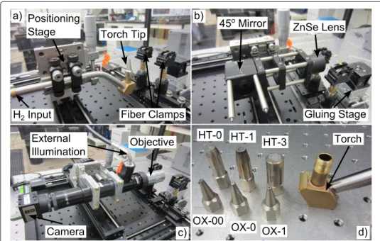
To produce tapered fibers, we use a heat-and-pull method in which a flame from a hydro-gen torch is used to soften or melt an optical fiber while simultaneously stretching it at a constant speed. In our system, we produce this flame using a custom-built mountable hydrogen torch, as seen in Figure 3a, which is threaded using a 7/16-24 die (McMaster-Carr, Part No. 26005A128) producing standard threads that allow for interchangeability of torch tips. The tips we use are the HT and OX series purchased from National Torch (see Figure 3d), which provide a wide variety of flame sizes useful for producing differ-ent sizes of tapered fibers. The hydrogen torch is fed by a needle valve-controlled line,
Table 1 Single mode cutoff diameters for tapered fibers in a number of situations
λ (nm) nco ncl
dc(nm)
WGA Numerical
637 1.47 1.00 452.6 452.6
1.47 1.33 778.8 778.9
780 1.47 1.00 554.1 554.2
1.47 1.33 953.6 953.7
1310 1.47 1.00 930.7 930.7
1.47 1.33 1601.6 1601.7
1550 1.47 1.00 1101.2 1101.2
1.47 1.33 1895.0 1895.1
Single mode cutoff diameter calculated using both the WGA approximation and numerical calculations for a green light (637 nm) observed in nitrogen vacancy photoluminescence [53] and near infrared light (780 nm) used in aqueous biosensing [54], as well as the dispersionless and low attenuation telecom wavelengths of 1310 nm and 1550 nm. All calculations are performed for both air-clad (ncl=1.0) and water-clad (ncl=1.33) environments. The appropriate
Figure 3 Tapered fiber puller.Pictures of the tapered fiber pulling apparatus witha)the hydrogen torch,b) the cage mounted ZnSe lens andc)the microscope imaging system mounted on the positioning gantry.d) Picture of the hydrogen torch along with the HT and OX series torch tips.
allowing for a very small and stable flame using the OX-00 torch tip, with a single 0.51 mm diameter hole. This tip is chosen because it produces compact tapers (less than 1 cm in total length) which are ideal for our fiber holders, while maintaining a relatively high transmission efficiency (up to∼80%).
Another method by which a fiber can be tapered is using a CO2laser, which produces radiation with a wavelength ranging from 10.2–10.8μm [44]. Absorption of these photons by an optical fiber causes it to heat in proportion to the intensity of the beam and the cross section of the fiber being irradiated. Therefore, the power of a CO2laser must be carefully controlled while pulling a fiber in order to ensure even heating. CO2lasers have also been used as a heat source for other processes, namely in the production of high-Q silica WGM resonators, such as microspheres [55] and bottles [56].
We integrate a CO2laser into our fiber pulling system by replacing our hydrogen torch with a cage mount system (see Figure 3b) containing a 45 degree cube-mounted silvered mirror (Thorlabs Product No. CM1P01) and a planoconvex ZnSe lens (Thorlabs -Product No. LA7542-F) with a focal length of 25.4 mm, which can be used to focus the intense, infrared radiation from the laser onto the fiber. Attaching our lens to the torch positioning system, we gain full control of its position. This allows for defocusing of the CO2laser beam, effectively controlling both the size and temperature of the hotspot on the fiber. Furthermore, the focused beam can be scanned along the fiber, allowing for a movable hotspot, which is required for bottle fabrication [54]. Finally, manual height adjustment of the cage mount focusing system allows us to ensure that the CO2beam will hit the center of the lens, reducing aberration.
It is also possible to attach a microscope imaging system directly to our torch posi-tioning gantry, as shown in Figure 3c. The microscope is comprised of a 10X M Plan Apo long working distance infinity-corrected objective (Edmund Optics - Stock No. #59-877) attached to an Optem Zoom 70XL lens system, allowing for 70× magnifi-cation of the setup. This image is recorded using an Edmund Optics EO-5012C color USB webcam, providing a video feed to a nearby computer. To ensure proper light-ing and image quality, light from an external Metaphase MP-LED-150 microscope LED illuminator is coupled into the lens system’s coaxial illumination port using a fiber optic waveguide (Edmund Optics - Stock No. #39-368). This system is very useful, as it allows for real time imaging of our completed tapered fibers (and other fabricated optical components) when dimpling or attaching it to its holder, with full three-axis control.
As tapered fibers are quite fragile, it is difficult to move them without breaking. For this reason, we first attach the tapered fiber to a holder, creating a more robust system which can easily be relocated. To this end, we have also included a manually adjusted Newport Compact Dovetail DS40-XYZ three-dimensional linear positioning stage in our system, which allows for 1μm sensitivity over a travel range of 14 mm in each ofxandyand 5 mm inz. This stage allows us to properly position and align the fiber holder, as well as gradually approach it to the fiber for gluing. In addition, it is used to position the fiber mold used in the dimpling process, which must be approached and raised precisely at the thinnest point of the tapered fiber.
splice - Part No. FIS114012), in which two straight cleaved fiber ends are butt coupled to each other with the aid of index matching gel (Fiber Instrument Sales matching gel - Part No. F10001V). Likewise, the fiber is mechanically spliced on its opposite end to a patch cable connected to a New Focus Model 1811 IR DC-125 MHz low noise photoreceiver. The DC signal from this photodiode is split off and recorded using an NI USB-6259 BNC DAQ card for the duration of a fiber pull, providing a record of transmission vs pull time, as seen in Figure 4.
Fiber tapering procedure
To create tapered fibers, we begin with a Corning SMF-28e optical fiber that has a silica core and cladding diameter of 8.2μm and 125μm, respectively, all of which is protected by an acrylate coating which extends out to a diameter of 245μm. The indices of refrac-tion and dimensions of the core and cladding are chosen such that this original fiber is single mode for wavelengths exceeding 1260 nm, which includes both the dispersionless and minimum loss wavelengths in silica of 1310 nm and 1550 nm, respectively.
To begin the tapering process, the acrylate coating is removed using a Micro-Strip® stripping tool over a region approximately 3 cm long in the center of an SMF-28e fiber around one meter in total length. This section of stripped fiber is subsequently cleaned using a solvent to remove any remaining acrylate. The tapering occurs in this stripped region, where the flammable acrylate has been removed. In addition, the two ends of the fiber are stripped of acrylate and cleaved flat using an Ericsson EFC11 fiber cleaver. Utilizing the mechanical splicers and index matching gel described above, these cleaved ends are spliced to two ends of a severed FC/APC patch cable, one of which leads to the photodiode, the other to the diode laser. This method of fiber splicing is ideal for this application, as it is quick and easy, allowing for a convenient input and removal of the tapering fiber to and from the optical circuit. Losses vary depending on fiber alignment for this splicing method, but we are only concerned with providing enough power to observe variations in fiber transmission. Once we have ensured that the splices provide sufficient power to the photodiode, the fiber is
placed in the V-groove fiber holders, with the region prepared for tapering centered between them.
At this point, the hydrogen torch is lit using a butane lighter and gas flow is adjusted to ensure a steady flame about 1 cm high. This flame is then approached towards the fiber until a small (a few mm) section begins to glow, indicating that the fiber is in a molten state. Once this point has been reached, the two pulling stages move in opposite directions, each at a constant speed generally chosen to be 40μm/s.
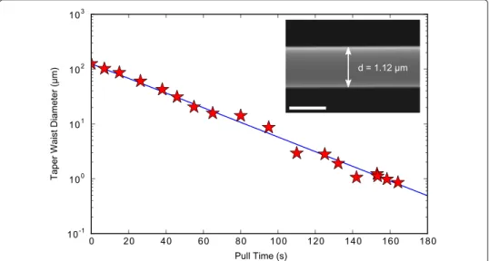
During each pull, the transmission through the fiber vs pull time is monitored, an example of which is presented in Figure 4 for the OX-00 torch tip. By monitoring fiber transmission, it is possible to determine the point at which the fiber waist has become single mode. This will be indicated as a stabilization of the fiber transmission (which is evident in Figure 4) due to the fact that the lossy, higher order modes of the fiber have died out, leaving behind the single fundamental mode of the fiber. Using images from a scanning electron microscope (SEM - inset of Figure 5), we experimentally measured the diameters of our fibers at the single mode transition to be∼1.1μm, consistent with the theoretically predicted diameter for an air-clad fiber with an index of 1.47 (we expect our fibers to have an index of 1.4677) at 1550 nm (see Table 1). By measuring the time required to reach this transition from a single pull, it is possible to determine a value for the hot-zone lengthLby inverting Eq. 1, provided that the pull speed and initial fiber diameter are knowna priori. Using this parameter, we are able to predict the fiber waist diameter for a given pull time. Note that in order for this prediction to be accurate, care must be taken to ensure that all subsequent pulls have conditions matching the original one in order to ensure a consistent hot-zone length. This is readily accomplished using our system. A plot of fiber waist diameter vs pull time using the apparatus described here is presented in Figure 5, indicating excellent agreement between the hot-zone length of
1.30 mm determined using the single mode cutoff point and the fit value of 1.29 mm. This ability to predict the fiber waist diameter is useful, as it allows for fabrication of fibers whose diameters support a propagating mode that is phase matched with the resonance we are interested in, enhancing coupling of light from the tapered fiber to the optical resonator [37].
At the point of single mode transition, the fiber waist diameter is small enough to pro-duce the desired evanescent field required for coupling to an optical cavity, which can be seen in the inset of Figure 4. However, it is often advantageous to continue pulling fibers to smaller diameters, further increasing the extent of the evanescent field outside the fiber geometry, allowing for a larger range of coupling before the fiber contacts the optical resonator. It is possible to create these sub-μm diameter fibers by continuing to pull for a small amount of time (∼10 s) after the single mode transition has been reached. Using the OX-00 torch tip, diameters as small as 850 nm can be achieved before the fiber breaks due to the pressure of the flowing hydrogen gas from the torch. By using the HT-3, our largest torch tip, the flame size increases, nearly doubling the hot-zone to 2.4 mm, allowing for the fabrication of tapered fibers with diameters down to 500 nm and 98% transmission. This provides fibers with diameters small enough that they can be used as a probe of nitrogen vacancy center photoluminescence [55], as well as allow single mode guiding of 780 nm light (Table 1), which is used in aqueous biosensing applications [56].
By monitoring transmission before and after the pull, it is also possible to determine the losses induced in the fiber due to the tapering process. This is important for determining the amount of power injected into the optical resonator, allowing for calculation of the number of photons confined in the optical resonator. For the OX-00 tip, a tapered fiber transmission efficiency of up to∼80% is achieved. By using the HT-3 tip, with its larger hot-zone, a more adiabatic taper transition region is created allowing us to produce fiber tapers with transmission efficiencies exceeding 99%, which is on par with state-of-the-art, ultralow loss fiber pullers [45].
Fiber dimpling procedure
Once a tapered fiber has been pulled, it is possible to proceed with the dimpling proce-dure. We begin by taping a stripped Corning SMF-28e optical fiber to thexyz-positioning stage located opposite the hydrogen torch, mounting it perpendicular to the tapered fiber so that it can be used as a mold in the dimpling process (see Figure 6a). The fiber mold is prepared by stripping off its acrylate coating and cleaning it with a solvent, producing a mold of 125μm in diameter. In addition, graphite powder (SLIP Plate® Tube-O-Lube®) is applied to the fiber mold to prevent it from sticking to the tapered fiber. This graphite generally burns away when introduced to the hydrogen flame during the dimple anneal-ing process, however, usanneal-ing too much graphite should be avoided as it can contaminate the dimple, inducing losses. To prevent this from happening, a fiber wipe or compressed air can be used to gently remove excess graphite.
Top View
a)
b)
c)
d)
f)
1.00.5
600 400
200 0
0
H2
Touched Released
Time (s)
Norm. Trans.
e)
Fiber Mold
Front View
Figure 6 Dimpling procedure.Schematics and microscope images illustrating the tapered fiber dimpling procedure. All scale bars are 125μm.a)The fiber is detensioned slightly (by about 10μm) by moving the fiber mounts inward, producing a small protrusion at the fiber’s thinnest point. The fiber mold is then adjusted such that it is aligned with this section of the fiber.b)The fiber mold is raised approximately 5 mm allowing the tapered fiber to wrap around it. The fiber mounts are gradually moved inwards as to prevent the fiber from breaking, while still maintaining tension on the fiber mold.c)An inverted hydrogen torch with a large flame (using HT series torch tip) is approached by hand, annealing the tapered fiber into a dimpled shape.d)The fiber mold is lowered while the fiber mounts are moved outwards to restore tension to the newly formed dimple. The dimple is gently removed from the fiber mold by flowing low pressure hydrogen gas from below.e)Optical microscope image of the resulting dimpled tapered fiber using this procedure.f) Plot indicating transmission (normalized to the pre-dimpled value) through the tapered fiber before and after dimpling. Losses induced by introducing the dimple to the fiber are around 8%.
thez-positioning stage. The mold fiber is then raised approximately 5 mm, while simulta-neously detensioning the tapered fiber, allowing the fiber to wrap itself around the mold producing the desired dimpled shape, as shown in Figure 6b. During this process, the tapered fiber should remain tensioned tightly around the mold at all times to prevent it from twisting.
Gluing procedure
Once a dimpled tapered fiber (or other optical component created by the fiber heating system) is produced, it must be carefully attached to its holder using the gluing apparatus. To begin this process, Devcon 5 Minute® epoxy gel (No. 14240) is applied to both sides of the fiber holder, which can be seen in Figure 7a. Care is taken to ensure that both droplets of epoxy are approximately the same height, ensuring that they will contact both sides of the tapered region at the same time. Once the epoxy is applied to the fiber holder, it is placed on its holding plate located on the gluing apparatus. The fiber holder is then carefully aligned beneath the fiber, ensuring that the fiber will be glued in the appropriate place. Next, the fiber holder is slowly raised using thez-axis of the positioning stages until the fiber has been enveloped in epoxy on both sides of the taper. This initial epoxy is then left to dry (for about 30 minutes) allowing the fiber to be rigidly held on the fiber holder, drastically increasing its durability. Once the initial epoxy dries, a second round of gluing is typically applied to the fiber, which increases the strength of the fiber’s attachment to the holder.
This entire gluing process is monitored in real time using the microscope imaging sys-tem mounted on the positioning gantry, which is very helpful as we are able to definitively determine the point at which the fiber has been glued. As well, by imaging the tapered region, along with monitoring transmission down the fiber, we can determine whether or not the tapered fiber has survived the gluing process. Once the fiber has been properly glued in place, it can be transferred directly to the coupling chamber where it is fusion spliced to an existing optical circuit, allowing for injection of light into optomechanical devices.
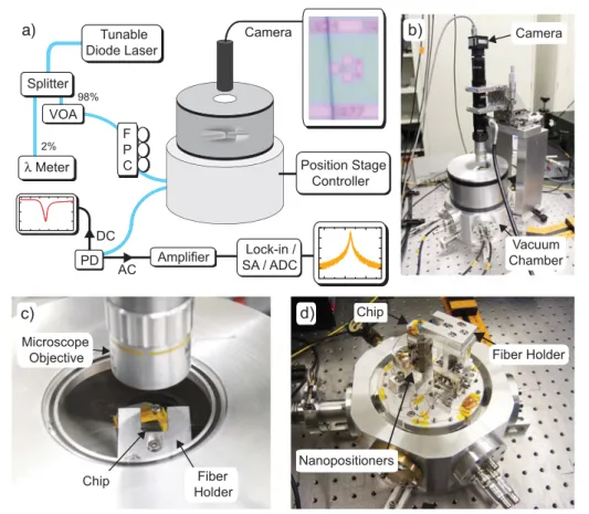
Optomechanical coupling chambers
Our coupling chambers, which can be seen in Figure 8b-d, use two separate position-ing stage arrangements, each of which have similar principles but different translation
Fiber Holder Fiber Clamp Dimple
Microscope
Epoxy
Top View
a)
b)
c)
Figure 7 Dimpled fiber gluing.a)Labeled schematic of the fiber gluing process. Once the
Figure 8 Optomechanical coupling chamber.a)Schematic of the optomechanical coupling chamber. The resonance lineshape from an optical cavity measured by monitoring the DC component of the fiber’s transmission while sweeping the laser frequency across one of its resonances is shown in the bottom left in red. Likewise, mechanical resonance data measured using the spectrum analyzer (SA) is presented on the bottom right in yellow. In the top right is a picture taken with our microscope imaging system of a dimpled fiber coupled to a torsional optomechanical device. As well, an angled SEM image of the same device (not to scale) is overlaid on the chamber. FPC - fiber polarization controller, VOA - variable optical attenuator, ADC - analog-to-digital converter, PD - photodiode.b)Picture of our optomechanical coupling chamber viewed from the outside while under vacuum.c)Close-up of the optical access port, illustrating how optomechanical coupling is observed.d)Picture of the inside of the chamber containing the Attocube ANPz/x nanopositioning stack, highlighting the positioning stages and fiber holder.
stages. In each case, the positioning systems are used to approach the optomechanical devices found on the sample chip to a dimpled tapered fiber glued to a stationary custom-machined fiber holder. The fiber was chosen to remain fixed as it is far less stable than the devices on the chip, so its mechanical noise is reduced by anchoring it to an immobile fiber holder.
the chip containing our optomechanical devices is mounted on a custom-built platform, which is attached to the vertical translation stage providing full three-axis control. These stages provide 50 nm stepping resolution over their entire travel range of 12 mm. Each of these systems have different strengths, with the Attocube stack providing extremely precise positioning over a relatively large range, while the Agilis stages provide a more durable, inexpensive alternative with a larger range of motion.
To allow interchangeability between our two chambers, this positioning system is fas-tened to a custom-machined circular plate, containing 1/4-20 tapped holes in a square pattern with a spacing of 3/4. This plate is then screwed onto a homemade aluminum base with 6 ports, each of which is sealed with an O-ring and provide electrical and optical input/output for the setup, as well as allowing for pressure control inside the chamber.
The optical input/output port consists of fiber feedthroughs, each of which allows for both an input and output fiber, channelling light to and from the tapered fiber. Each fiber is glued in place using Varian Torr Seal high vacuum epoxy, which provides the appropriate seal required for vacuum. For the Attocube setup, the electrical port houses three hermetically sealed BNC feedthroughs. The other type of electrical port, which provides input/output for the Agilis stages, is comprised of a vacuum compatible 15-pin D-type connector housed in a KF50 feedthrough flange (Accu-Glass Products - Model No. 15D-K50).
The vacuum environment provided by our coupling chambers removes airborne con-taminants which can reduce the quality of the tapered fiber and optomechanical devices over time [57]. It is also possible to remove such contaminants using a nitrogen purged environment [49], however, performing optomechanics in vacuum has the added advan-tage of increasing the mechanical quality factors of devices by drastically reducing viscous damping [58]. The vacuum pump port is comprised of a KF25 adapter connected to a turbo pump backed by a dry scroll pump. By using a completely dry pumping system, we ensure that no oil is ever backstreamed into our system. This connection is made using vibration isolating bellows, which are passed through a cement block to further pre-vent vibrations from the pump reaching the optical table where the chamber is located. Using this pumping system, we can achieve chamber pressures as low as 10−6torr. There also exists a release port, consisting of a Nupro B-4HK brass bellows-sealed valve, which allows for surrounding air to enter the system, re-establishing ambient pressure inside the chamber. All unused ports on the chamber base are covered with a blank port. This entire system is leak-checked using an Adixen ASM380 dry leak detector, ensuring it is properly sealed.
chip are imaged using the exact same imaging system described above for the tapered fiber puller. This is made possible by the fact that this microscope is oriented using a three dimensional arrangement of manually positioned New Focus 9063-COM gothic-arch translation stages mounted on a two legged custom-built stand with identical mounting plate to that used for manualz-positioning of the hydrogen torch in the tapered fiber puller, allowing interchangeability of the microscope between the two systems. The Mitu-toyo No. 906912 micrometers used to manipulate this positioning system, provide a 25 mm travel range with 10μm resolution. This resolution is more than enough to view our devices in thexy-plane of the chip, as well as provide excellent focusing for our imaging setup.
On-chip optomechanical devices
Due to the small feature sizes required for our optomechanical devices, we have cho-sen to use foundry-based nanofabrication, which provides high throughput of devices with a minimum feature size of 100 nm using top-down DUV photolithography [29]. Each optomechanical device consists of an optical microdisk side-coupled to a mechan-ical nano/micro-resonator, such as a torsion paddle or a cantilever, as can be seen in Figure 9. Each device is centered in a large etched area (approximately 100μm×50μm), which provides ample room for coupling using our dimpled tapered fiber method. The mask for these devices is designed using custom-programmed Python scripts utilizing the gdspy module, which generates a GDSII file containing our chip layout. This allows us to iterate through a number of device specifications, such as coupling gap, disk radius and mechanical resonator dimensions, providing a large parameter space in which we can explore different optomechanical regimes. These design files are then submitted through Canadian Microelectronic Corporation (CMC) Microsystems to the Interuniver-sity Microelectronics Center (IMEC) located in Leuven, Belgium. It is here our devices are fabricated on an 8 inch silicon-on-insulator (SOI) wafer, which consists of a 220 nm
thick layer of single crystal silicon supported by a 2μm layer of silicon dioxide. The single crystal silicon device layer is ideal for optomechanical devices, as it has negligible absorp-tion in the telecom band around 1550 nm and a high index of refracabsorp-tion (n ≈ 3.42), enhancing the mechanical resonator’s perturbation of the optical cavity’s evanescent field. Our devices are patterned onto this wafer using an excimer laser (193 nm - 248 nm) and high-definition photomasks derived from our design files. These patterned wafers are then etched using either a standard or high dose recipe, producing optomechanical devices in the silicon layer which are held rigidly in place by the oxide buffer. This, along with a protective resist coating the entire wafer, help to prevent damage to the devices during transit.
After we receive these wafers, a number of post-processing procedures must be per-formed in order to prepare our devices for measuring. We begin by dicing the 8 inch wafer into 1 cm× 1 cm chips using a diamond saw. Each chip is then ultrasonically cleaned with acetone and rinsed with isopropyl alcohol to remove the protective coating. Once the wafer has been diced and cleaned, a buffered oxide etch (BOE) is used to selectively remove the sacrificial oxide layer beneath our mechanical devices, which releases them, allowing them to oscillate freely. It is important to note that since BOE is a wet etch, we must ensure that our devices are dried using either a critical point drier or ultralight sol-vents, such as n-Pentane (C5H12), to prevent stiction. Once a chip has been etched and dried, it is ready to be placed in the chamber for measuring.
Coupling procedure
Coupling to our optomechanical devices begins by locating the dimple of the tapered fiber using the imaging apparatus. This is done by searching for the portion of the fiber that is in focus at the lowest point (due to the fact that the dimple protrudes away from the rest of the fiber). Once the dimple is found, the nanopositioning stages are used to align the desired optomechanical device such that the lowest point of the dimple is able to couple light into the optical resonator.
The precision of our nanopositioning stack allows for two methods by which we can couple light into the modes of our optical resonators. We can either bring the fiber close enough to the device such that the cavity’s optical modes are excited by the fiber’s evanes-cent field or we can simply touch the fiber to the optical resonator. Hovering has the advantage that the excited optical modes are less perturbed by the fiber’s presence, result-ing in reduced losses. However, by touchresult-ing the fiber to the resonator, the mechanical instability of the fiber is further reduced. As well, by using this coupling method, it is pos-sible to excite a larger number of optical modes, some of which have higherQs and larger optomechanical coupling to the mechanical resonator.
Results and discussion
Data acquisition: side-of-fringe and homodyne detection
the “tuned-to-the-slope” regime [59], which is illustrated in Figure 10a. In this detection scheme, the cavity resonance shift due to the mechanical resonator’s motion is trans-duced by the slope of the optical lineshape into AC transmission fluctuations in the fiber, occurring at the mechanical resonance frequency. Therefore, by tuning our probe laser wavelength to the maximal slope of our optical cavity resonance, we provide optimal optomechanical transduction efficiency, as can be seen in Figure 10b. In general, this res-onant enhancement scales with the system’s optical quality factor which increases the slope of the resonance, however, this is convolved with other effects such as an optical mode’s volume and overlap with mechanical motion [21]. Using the experimental setup shown in Figure 8a to perform this type of measurement, we have probed devices with an angular resolution of 4 nrad/√Hz corresponding to a torque transduction on the level of 4×10⁻²⁰N·m/√Hz [21], as well as displacement noise floors of 2 fm/√Hz and force sensitivity of 132 aN/√Hz [18].
It is also possible to perform phase-sensitive measurements on our devices in the “tuned-to-the-peak” regime using a balanced optical homodyne detection system [60], which can be used for quadrature and entanglement measurements [61]. This method of detection also has a number of advantages, including cancellation of laser noise [62] and the ability to lock the laser to the bottom of the optical resonance [17]. Furthermore, since the laser’s detuning from the cavity resonance is zero, a maximum number of photons are coupled into the cavity, which enhances the system’s optomechanical coupling.
After setting up one of these detection schemes, the AC transmission signal through the fiber is sent to a spectrum analyzer (SA), which outputs its frequency power spec-trum. For an optomechanical signal, this includes the power spectral density (PSD) of the mechanical motion [63].
Figure 10 Optomechanical data acquisition.a)Schematic of the mechanism by which
“tuned-to-the-slope” cavity optomechanical detection is performed. We begin with an unperturbed optical cavity, with a resonance lineshape (solid, blue) centered atω0. The periodic displacementxof the
Alternatively, a time series measurement of the voltage signal taken with an analog-to-digital converter (ADC) can be analog-to-digitally analyzed to determine its spectral components. In our system, this is performed using a digital lock-in amplifier (Zurich Instruments HF2LI), which is a specialized ADC that first mixes an input voltage signal with a refer-ence frequency,ωref, shifting the frequencies of the input signal by±ωref. Therefore the frequency information around the reference frequency of the input signal is now the low frequency component of the mixed signal. This has the advantage of requiring a data col-lection rate proportional to the bandwidth of the signal measurement, as opposed to a data collection rate proportional to the maximum frequency component. For example, when bandwidth of only 100 kHz centered at 10 MHz contains important spectral infor-mation, a data collection rate of ∼105samples per second (SPS) can be used as opposed to a rate of∼107SPS, a reduction of about 100 times the data needed to acquire the signal of interest.
After mixing, the lock-in applies a low-pass filter to reduce noise contributions from unwanted frequencies outside the measurement bandwidth, thus the time series output of a lock-in amplifier is the result of a convolution of the lock-in amplifier’s filter response with the demodulated input signal,i.e.
Z(t)=X(t)+iY(t)= {H(t)∗eiωreftV(t)}(t), (6)
whereX(t)andY(t)are the two outputs of a dual-phase lock-in amplifier, H(t) is the impulse response of the lock-in amplifier’s filter, andV(t)is the input signal to the lock-in. Fourier transforming the output elucidates the convolution, giving
Z(ω)=H(ω)V(ω−ωref). (7)
Thus the spectrum of the lock-in amplifier’s output is the spectrum of the input voltage translated in frequency by the reference frequency and enveloped by the lock-in ampli-fier’s filter. The power spectrum can then be estimated by takingSZZ(ω) = |Z(ω)|2, or done in practice by using a PSD estimation algorithm such as Bartlett’s method [64], giving
SZZ(ω)= |H(ω)|2SVV(ω−ωref). (8)
This method of data acquisition allows for real time optimization of optomechani-cal transduction in our devices, which facilitates sensitive probing of their mechanioptomechani-cal motion, allowing for precise measurements of physical quantities, such as forces [18] and torques [21].
Conclusion
by high precision, nanopositioning stages. By using the amplitude sensitive “tuned-to-the-slope” detection scheme, angular resolution of 4 nrad/√Hz [21] and displacement transduction of 2 fm/√Hz [18] have already been demonstrated. It is anticipated that using this technique for optomechanical coupling, we will be able to continue to measure increasingly sensitive devices, approaching the measurement limits imposed by quantum mechanics [59].
Competing interests
The authors declare that they have no competing interests.
Authors’ contributions
BDH, PHK and JPD conceived and designed the experiment. BDH, PHK and AJRM constructed the experiment. PHK performed nanofabrication post-processing for the on-chip devices. BDH, PHK, CD, AJRM and HR collected and analyzed data. BDH and AJRM performed theoretical calculations regarding the single mode cutoff diameter for tapered fibers. CD and PHK developed and optimized the procedure for producing dimpled tapered fibers. CD and HR created software for data taking and system manipulation. BDH, PHK, CD and JPD drafted the manuscript. All authors have read, approved and provided critical revisions for the final manuscript.
Acknowledgements
The authors would like to thank Prof. Paul Barclay for numerous helpful suggestions and insight into both the theoretical and practical applications of optomechanics. We would also like to thank Don Mullin, Devon Bizuk and Greg Popowich for technical assistance. This work was supported by the University of Alberta, Faculty of Science; the Natural Sciences and Engineering Research Council of Canada; Alberta Innovates Technology Futures; the Canada Foundation for Innovation; and the Alfred P. Sloan Foundation.
Received: 21 January 2014 Accepted: 2 April 2014 Published: 29 April 2014
References
1. Krause AG, Winger M, Blasius TD, Lin Q, Painter O:A high-resolution microchip optomechanical accelerometer.
Nat Photon2012,6:768–772.
2. Schmid S, Dohn S, Boisen A:Real-time particle mass spectrometry based on resonant micro strings.Sensors 2010,10:8092–8100.
3. Yang YT, Callegari C, Feng XL, Ekinci KL, Roukes ML:Zeptogram-scale nanomechanical mass sensing.Nano Lett 2006,6:583–586.
4. Jensen K, Kim K, Zettl A:An atomic-resolution nanomechanical mass sensor.Nat Nanotech2008,3:533–537. 5. Chaste J, Eichler A, Moser J, Ceballos G, Rurali R, Bachtold A:A nanomechanical mass sensor with yoctogram
resolution.Nat Nanotech2012,7:301–304.
6. Li M, Tang HX, Roukes ML:Ultra-sensitive NEMS-based cantilevers for sensing, scanned probe and very
high-frequency applications.Nat Nanotech2007,2:114–120.
7. Cleland AN, Roukes ML:A nanometre-scale mechanical electrometer.Nature1998,392:160–162.
8. Larsen T, Schmid S, Grönberg L, Niskanen AO, Hassel J, Dohn S, Boisen A:Ultrasensitive string-based temperature
sensors.Appl Phys Lett2011,98:121901.
9. Zhang XC, Myers EB, Sader JE, Roukes ML:Nanomechanical torsional resonators for frequency-shift infrared
thermal sensing.Nano Lett2013,13:1528–1534.
10. Gavartin E, Verlot P, Kippenberg TJ:A hybrid on-chip optomechanical transducer for ultrasensitive force
measurements.Nat Nanotech2012,7:509–514.
11. Moser J, Güttinger J, Eichler A, Esplandiu MJ, Liu DE, Dykman MI, Bachtold A:Ultrasensitive force detection with a
nanotube mechanical resonator.Nat Nanotech2013,8:493–496.
12. Fritz J, Baller MK, Lang HP, Rothuizen H, Vettiger P, Meyer E, Güntherodt H-J, Gerber Ch, Gimzewski JK:Translating
biomolecular recognition into nanomechanics.Science2000,288:316–318.
13. Mertens J, Rogero C, Calleja M, Ramos D, Martín-Gago JA, Briones C, Tamayo J:Label-free detection of DNA
hybridization based on hydrationinduced tension in nucleic acid films.Nat Nanotech2008,3:301–307.
14. Ndieyira JW, Watari M, Barrera AD, Zhou D, Vögtli M, Batchelor M, Cooper MA, Strunz T, Horton MA, Abell C, Rayment T, Aeppli G, McKendry RA:Nanomechanical detection of antibiotic-mucopeptide binding in a model for
superbug drug resistance.Nat Nanotech2008,3:691–696.
15. Gupta A, Akin D, Bashir R:Single virus particle mass detection using microresonators with nanoscale
thickness.Appl Phys Lett2004,84:1976–1978.
16. Arcizet O, Cohadon P-F, Briant T, Pinard M, Heidmann A, Mackowski J-M, Michel C, Pinard L, Français O, Rousseau L:
High-sensitivity optical monitoring of a micromechanical resonator with a quantum-limited
optomechanical sensor.Phys Rev Lett2006,97:133601.
17. Schliesser A, Anetsberger G, Rivière R, Arcizet O, Kippenberg TJ:High-sensitivity monitoring of micromechanical
vibration using optical whispering gallery mode resonators.New J Phys2008,10:095015.
18. Doolin C, Kim PH, Hauer BD, MacDonald AJR, Davis JP:Multidimensional optomechanical cantilevers for high
frequency atomic force microscopy.New J Phys2014,16:035001.
19. Stapfner S, Ost L, Hunger D, Reichel J, Favero I, Weig EM:Cavity-enhanced optical detection of carbon nanotube
20. Eichenfield M, Camacho R, Chan J, Vahala KJ, Painter O:A picogram- and nanometre-scale photonic-crystal
optomechanical cavity.Nature2009,459:550–555.
21. Kim PH, Doolin C, Hauer BD, MacDonald AJR, Freeman MR, Barclay PE, Davis JP:Nanoscale torsional
optomechanics.Appl Phys Lett2013,102:053102.
22. Hossein-Zadeh M, Hossein R, Hajimiri A, Vahala KJ:Characterization of a radiation-pressure-driven
micromechanical oscillator.Phys Rev A2006,74:023813.
23. Kippenberg TJ, Vahala KJ:Cavity optomechanics: Back-action at the mesoscale.Science2008,321:1172–1176. 24. Jayich AM, Sankey JC, Zwickl BM, Yang C, Thompson JD, Girvin SM, Clerk AA, Marquardt F, Harris JGE:Dispersive
optomechanics: a membrane inside a cavity.New J Phys2008,10:095008.
25. Favero I, Stapfner S, Hunger D, Paulitschke P, Reichel J, Lorenz H, Weig EM, Karrai K:Fluctuating nanomechanical
system in a high finesse optical microcavity.Opt Express2009,17:12813–12820.
26. Anetsberger G, Arcizet O, Unterreithmeier QP, Rivière R, Schliesser A, Weig EM, Kotthaus JP, Kippenberg TJ:
Near-field cavity optomechanics with nanomechanical oscillators.Nat Phys2009,5:909–914.
27. Park Y-S, Wang H:Resolved-sideband and cryogenic cooling of an optomechanical resonator.Nat Phys2009,
5:489–493.
28. Teufel JD, Li D, Allman MS, Cicak K, Sirois AJ, Whittaker JD, Simmonds RW:Circuit cavity electromechanics in the
strong-coupling regime.Nature2011,471:204–208.
29. Selvaraja SK:Wafer-scale fabrication technology for silicon photonic integrated circuits.PhD thesis, Ghent University, Faculty of Engineering, Department of Information; 2011.
30. Manfrinato VR, Zhang L, Su D, Duan H, Hobbs RG, Stach EA, Berggren KK:Resolution limits of electron-beam
lithography toward the atomic scale.Nano Lett2013,13:1555–1558.
31. Winger M, Blasius TD, Alegre TPM, Safavi-Naeini AH, Meenehan S, Cohen J, Strobbe S, Painter O:A chip-scale
integrated cavity-electro-optomechanics platform.Opt Express2011,19:24905–24921.
32. Michael CP, Borselli M, Johnson TJ, Chrystal C, Painter O:An optical fiber-taper probe for wafer-scale
microphotonic device characterization.Opt. Express2007,15:4745–4752.
33. Fiore V, Yang Y, Kuzyk MC, Barbour R, Tian L, Wang H:Storing optical information as a mechanical excitation in a
silica optomechanical resonator.Phys Rev Lett2011,107:133601.
34. Li M, Pernice WHP, Xiong C, Baehr-Jones T, Hochberg M, Tang HX:Harnessing optical forces in integrated
photonic circuits.Nature2008,456:480–484.
35. Gröblacher S, Hill JT, Safavi-Naeini AH, Chan J, Painter O:Highly efficient coupling from an optical fiber to a
nanoscale silicon optomechanical cavity.Appl Phys Lett2013,103:181104.
36. Cohen JD, Meenehan SM, Painter O:Optical coupling to nanoscale optomechanical cavities for near
quantum-limited motion transduction.Opt Express2013,21:11227–11236.
37. Knight JC, Cheung G, Jacques F, Birks TA:Phase-matched excitation of whispering-gallery-mode resonances
by a fiber taper.Opt Lett1997,22:1129–1131.
38. Cai M, Painter O, Vahala KJ:Observation of critical coupling in a fiber taper to a silica-microsphere
whispering-gallery mode system.Phys Rev Lett2000,85:74–77.
39. Barclay PE, Srinivasan K, Borselli M, Painter O:Efficient input and output fiber coupling to a photonic crystal
waveguide.Opt Lett2004,29:697–699.
40. Srinivasan K, Miao H, Rakher MT, Davanço M, Aksyuk V:Optomechanical transduction of an integrated silicon
cantilever probe using a microdisk resonator.Nano Lett2011,11:791–797.
41. Zhang EJ, Sacher WD, Poon JKS:Hydrofluoric acid flow etching of low-loss subwavelength-diameter biconical
fiber tapers.Opt Express2010,18:22593–22598.
42. Laine J-P, Little BE, Haus HA:Etch-eroded fiber coupler for whispering-gallery-mode excitation in high-Q silica
microspheres.IEEE Photon Technol Lett1999,11:1429–1430.
43. Brambilla G, Finazzi V, Richardson DJ:Ultra-low-loss optical fiber nanotapers.Opt Express2004,12:2258–2263. 44. Ward JM, O’Shea DG, Shortt BJ, Morrissey MJ, Deasy K, Chormaic SGN:Heat-and-pull rig for fiber taper
fabrication.Rev Sci Instrum2006,77:083105.
45. Ding L, Belacel C, Ducci S, Leo G, Favero I:Ultralow loss single-mode silica tapers manufactured by a
microheater.Appl Opt2010,49:2441–2445.
46. Tong L, Gattass RR, Ashcom JB, He S, Lou J, Shen M, Maxwell I, Mazur E:Subwavelength-diameter silica wires for
low-loss optical wave guiding.Nature2003,426:816–819.
47. Birks TA, Li YW:The shape of fiber tapers.J Lightwave Technol1992,10:432–438. 48. Arnaud JA:Beam and Fiber Optics. New York: Academic Press; 1976.
49. Borselli M:High-Q microresonators as lasing elements for silicon photonics.PhD thesis, California Institute of Technology, Department of Applied Physics; 2006.
50. Jackson JD:Classical Electrodynamics. New York: Wiley; 1999. 51. Gloge D:Weakly guiding fibers.Appl Opt1971,10:2252–2258.
52. Srinivasan K, Barclay PE, Borselli M, Painter OJ:An optical-fiber-based probe for photonic crystal microcavities.
EE J Sel Area Comm2005,23:1321–1329.
53. Collot L, Lefèvre-Seguin V, Brune M, Raimond JM, Haroche S:Very high-Q whispering-gallery mode resonances
observed on fused silica microspheres.Europhys Lett1993,23:327–334.
54. Pöllinger M, O’Shea D, Warken F, Rauschenbeutel A:Ultrahigh-Q tunable whispering-gallery-mode
microresonator.Phys Rev Lett2009,103:053901.
55. Fu K-MC, Barclay PE, Santori C, Faraon A, Beausoleil RG:Low-temperature tapered-fiber probing of diamond
nitrogen-vacancy ensembles coupled to GaP microcavities.New J Phys2011,13:055023.
56. Dantham VR, Holler S, Kolchenko V, Wan Z, Arnold S:Taking whispering gallery-mode single virus detection
and sizing to the limit.Appl Phys Lett2012,101:043704.
57. Fujiwara M, Toubaru K, Shigeki T:Optical transmittance degradation in tapered fibers.Opt Express2011,
58. Verbridge SS, Ilic R, Craighead HG, Parpia JM:Size and frequency dependent gas damping of nanomechanical
resonators.Appl Phys Lett2008,93:013101.
59. Braginsky VB, Khalili FYa:Quantum Measurement. Cambridge: Cambridge University Press; 1995. 60. Yuen HP, Chan VWS:Noise in homodyne and heterodyne detection.Opt Lett1983,8:177–179.
61. Laurat J, Keller G, Oliveira-Huguenin JA, Fabre C, Coudrea T, Serafini A, Adesso G, Illuminati F:Entanglement of
two-mode Gaussian states: characterization and experimental production and manipulation.J Opt B:
Quantum Semiclass Opt2005,7:577–587.
62. Safavi-Naeini AH, Gröblacher S, Hill JT, Chan J, Aspelmeyer M, Painter O:Squeezed light from a silicon
micromechanical resonator.Nature2013,500:185–189.
63. Hauer BD, Doolin C, Beach KSD, Davis JP:A general procedure for thermomechanical calibration of
nano/micro-mechanical resonators.Ann Phys2013,339:181–207.
64. Bartlett MS:Smoothing periodograms from time-series with continuous spectra.Nature1948,161:686–687.
doi:10.1140/epjti4
Cite this article as:Haueret al.:On-chip cavity optomechanical coupling.EPJ Techniques and Instrumentation20141:4.
Submit your manuscript to a
journal and benefi t from:
7Convenient online submission 7Rigorous peer review
7Immediate publication on acceptance 7Open access: articles freely available online 7High visibility within the fi eld
7Retaining the copyright to your article