BCD-To-Decimal Decoder
Binary-To-Octal Decoder
The MC14028B decoder is constructed so that an 8421 BCD code
on the four inputs provides a decimal (one−of−ten) decoded output,
while a 3−bit binary input provides a decoded octal (one−of−eight)
code output with D forced to a logic “0”. Expanded decoding such as
binary−to−hexadecimal (one−of−sixteen), etc., can be achieved by
using other MC14028B devices. The part is useful for code
conversion, address decoding, memory selection control,
demultiplexing, or readout decoding.
Features
•
Diode Protection on All Inputs
•
Supply Voltage Range = 3.0 Vdc to 18 Vdc
•
Capable of Driving Two Low−power TTL Loads or One Low−Power
Schottky TTL Load Over the Rated Temperature Range
•
Positive Logic Design
•
Low Outputs on All Illegal Input Combinations
•
Similar to CD4028B
•
NLV Prefix for Automotive and Other Applications Requiring
Unique Site and Control Change Requirements; AEC−Q100
Qualified and PPAP Capable
•
This Device is Pb−Free and is RoHS Compliant
MAXIMUM RATINGS (Voltages Referenced to VSS)
Parameter Symbol Value Unit
DC Supply Voltage Range VDD − 0.5 to +18.0 V
Input or Output Voltage Range (DC or Transient)
Vin, Vout − 0.5 to VDD
+ 0.5
V Input or Output Current (DC or Transient)
per Pin
Iin, Iout ±10 mA
Power Dissipation per Package (Note 1) PD 500 mW Ambient Temperature Range TA − 55 to +125 °C Storage Temperature Range Tstg − 65 to +150 °C
Lead Temperature (8−Second Soldering) TL 260 °C
Stresses exceeding those listed in the Maximum Ratings table may damage the device. If any of these limits are exceeded, device functionality should not be assumed, damage may occur and reliability may be affected.
1. Temperature Derating: “D/DW” Packages: –7.0 mW/_C From 65_C To 125_C This device contains protection circuitry to guard against damage due to high static voltages or electric fields. However, precautions must be taken to avoid applications of any voltage higher than maximum rated voltages to this high−impedance circuit. For proper operation, Vin and Vout should be constrained
to the range VSS≤ (Vin or Vout) ≤ VDD.
Unused inputs must always be tied to an appropriate logic voltage level (e.g., either VSS or VDD). Unused outputs must be left open.
http://onsemi.com
See detailed ordering and shipping information in the package dimensions section on page 2 of this data sheet.
ORDERING INFORMATION
A = Assembly Location WL = Wafer Lot YY, Y = Year WW = Work Week G = Pb−Free Package
MARKING DIAGRAM
SOIC−16 D SUFFIX CASE 751B
1 16
14028BG AWLYWW
PIN ASSIGNMENT
13 14 15 16
9
10
11 12 5
4 3 2 1
8 7 6
C B Q1 Q3 VDD
Q8 A D Q7
Q0 Q2 Q4
VSS
Q6 Q5 Q9
TRUTH TABLE
D C B A Q9 Q8 Q7 Q6 Q5 Q4 Q3 Q2 Q1 Q0
0 0 0 0 0 0 0 0 0 0 0 0 0 1
0 0 0 1 0 0 0 0 0 0 0 0 1 0
0 0 1 0 0 0 0 0 0 0 0 1 0 0
0 0 1 1 0 0 0 0 0 0 1 0 0 0
0 1 0 0 0 0 0 0 0 1 0 0 0 0
0 1 0 1 0 0 0 0 1 0 0 0 0 0
0 1 1 0 0 0 0 1 0 0 0 0 0 0
0 1 1 1 0 0 1 0 0 0 0 0 0 0
1 0 0 0 0 1 0 0 0 0 0 0 0 0
1 0 0 1 1 0 0 0 0 0 0 0 0 0
1 0 1 0 0 0 0 0 0 0 0 0 0 0
1 0 1 1 0 0 0 0 0 0 0 0 0 0
1 1 0 0 0 0 0 0 0 0 0 0 0 0
1 1 0 1 0 0 0 0 0 0 0 0 0 0
1 1 1 0 0 0 0 0 0 0 0 0 0 0
1 1 1 1 0 0 0 0 0 0 0 0 0 0
BLOCK DIAGRAM
8421 BCD INPUTS
DECIMAL DECODED OUTPUTS OCTAL
DECODED OUTPUTS 3
14 2 15 1 6 7 4 9 5 A
B C D Q9
Q8 Q7 Q6 Q5 Q4 Q3 Q2 Q1 Q0 3-BIT
BINARY INPUTS
10 13 12 11
VDD = PIN 16
VSS = PIN 8
ORDERING INFORMATION
Device Package Shipping†
MC14028BDG SOIC−16
(Pb−Free)
48 Units / Rail
MC14028BDR2G SOIC−16
(Pb−Free)
2500 / Tape & Reel
NLV14028BDR2G* SOIC−16
(Pb−Free)
2500 / Tape & Reel
†For information on tape and reel specifications, including part orientation and tape sizes, please refer to our Tape and Reel Packaging Specifications Brochure, BRD8011/D.
*NLV Prefix for Automotive and Other Applications Requiring Unique Site and Control Change Requirements; AEC−Q100 Qualified and PPAP Capable.
ÎÎÎÎÎÎÎÎÎÎÎÎÎÎÎÎÎÎÎÎÎÎÎÎÎÎÎÎÎÎÎÎÎ ÎÎÎÎÎÎÎÎÎÎÎÎÎÎÎÎÎÎÎÎÎÎÎÎÎÎÎÎÎÎÎÎÎ
ELECTRICAL CHARACTERISTICS (Voltages Referenced to VSS)
Characteristic Symbol VDD Vdc
−55_C 25_C 125_C
Unit
Min Max Min
Typ
(Note 2) Max Min Max
Output Voltage “0” Level Vin = VDD or 0
“1” Level Vin = 0 or VDD
VOL 5.0 10 15 − − − 0.05 0.05 0.05 − − − 0 0 0 0.05 0.05 0.05 − − − 0.05 0.05 0.05 Vdc VOH 5.0 10 15 4.95 9.95 14.95 − − − 4.95 9.95 14.95 5.0 10 15 − − − 4.95 9.95 14.95 − − − Vdc
Input Voltage “0” Level (VO = 4.5 or 0.5 Vdc)
(VO = 9.0 or 1.0 Vdc)
(VO = 13.5 or 1.5 Vdc)
“1” Level (VO = 0.5 or 4.5 Vdc)
(VO = 1.0 or 9.0 Vdc)
(VO = 1.5 or 13.5 Vdc)
VIL 5.010
15 − − − 1.5 3.0 4.0 − − − 2.25 4.50 6.75 1.5 3.0 4.0 − − − 1.5 3.0 4.0 Vdc
VIH 5.010
15 3.5 7.0 11 − − − 3.5 7.0 11 2.75 5.50 8.25 − − − 3.5 7.0 11 − − − Vdc
Output Drive Current
(VOH = 2.5 Vdc) Source
(VOH = 4.6 Vdc)
(VOH = 9.5 Vdc)
(VOH = 13.5 Vdc)
(VOL = 0.4 Vdc) Sink
(VOL = 0.5 Vdc) (VOL = 1.5 Vdc)
IOH 5.0 5.0 10 15 –3.0 –0.64 –1.6 –4.2 − − − − –2.4 –0.51 –1.3 –3.4 –4.2 –0.88 –2.25 –8.8 − − − –1.7 –0.36 –0.9 –2.4 − − − − mAdc IOL 5.0 10 15 0.64 1.6 4.2 − − − 0.51 1.3 3.4 0.88 2.25 8.8 − − − 0.36 0.9 2.4 − − − mAdc
Input Current Iin 15 − ±0.1 − ±0.00001 ±0.1 − ±1.0 mAdc
Input Capacitance (Vin = 0) Cin − − − − 5.0 7.5 − − pF
Quiescent Current (Per Package) IDD 5.0
10 15 − − − 5.0 10 20 − − − 0.005 0.010 0.015 5.0 10 20 − − − 150 300 600 mAdc
Total Supply Current (Note 3, 4) (Dynamic plus Quiescent, Per Package)
(CL = 50 pF on all outputs, all
buffers switching)
IT 5.0
10 15
IT = (0.3 mA/kHz) f + IDD
IT = (0.6 mA/kHz) f + IDD
IT = (0.9 mA/kHz) f + IDD
mAdc
Product parametric performance is indicated in the Electrical Characteristics for the listed test conditions, unless otherwise noted. Product performance may not be indicated by the Electrical Characteristics if operated under different conditions.
2. Data labelled “Typ” is not to be used for design purposes but is intended as an indication of the IC’s potential performance. 3. The formulas given are for the typical characteristics only at 25_C.
4. To calculate total supply current at loads other than 50 pF: IT(CL) = IT(50 pF) + (CL – 50) Vfk where: IT is in mA (per package), CL in pF,
V = (VDD – VSS) in volts, f in kHz is input frequency, and k = 0.001. SWITCHING CHARACTERISTICS (Note 5)(CL = 50 pF, TA = 25_C)
Characteristic Symbol VDD Min
Typ
(Note 6) Max Unit
Output Rise and Fall Time
tTLH, tTHL = (1.5 ns/pF) CL + 25 ns
tTLH, tTHL = (0.75 ns/pF) CL + 12.5 ns
tTLH, tTHL = (0.55 ns/pF) CL + 9.5 ns
tTLH,
tTHL 5.0
10 15 − − − 100 50 40 200 100 80 ns
Propagation Delay Time
tPLH, tPHL = (1.7 ns/pF) CL + 215 ns
tPLH, tPHL = (0.66 ns/pF) CL + 97 ns
tPLH, tPHL = (0.5 ns/pF) CL + 65 ns
tPLH,
tPHL 5.0
10 15 − − − 300 130 90 600 260 180 ns
5. The formulas given are for the typical characteristics only at 25_C.
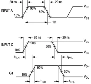
Figure 1. Dynamic Signal Waveforms
Inputs B, C, and D switching in respect to a BCD code.
Inputs A, B, and D low.
All outputs connected to respective CL loads. f in respect to a system clock.
20 ns 20 ns 90%
50% 10%
1/f
VDD
VSS
20 ns 20 ns INPUT A
INPUT C
Q4 10%
90% 50%
VDD
VSS
VOH VOL
tPLH tPHL
tTLH tTHL
50% 90%
10%
LOGIC DIAGRAM
Q9 Q8 Q7 Q6 Q5 Q4 Q3 Q2 Q1 Q0
D C B A
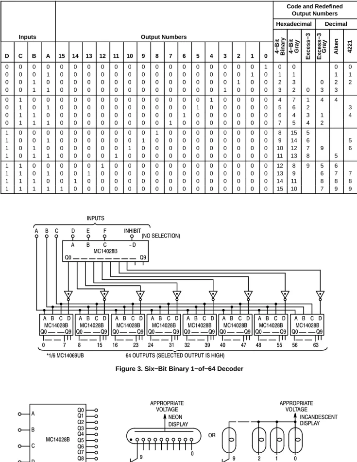
APPLICATIONS INFORMATION
Expanded decoding can be performed by using the
MC14028B and other CMOS Integrated Circuits. The
circuit in Figure 2 converts any 4−bit code to a decimal or
hexadecimal code. The accompanying table shows the input
binary combinations, the associated “output numbers” that
go “high” when selected, and the “redefined output
numbers” needed for the proper code. For example: For the
combination DCBA = 0111 the output number 7 is redefined
for the 4−bit binary, 4−bit gray, excess−3, or excess−3 gray
codes as 7, 5, 4, or 2, respectively. Figure 3 shows a 6−bit
binary 1−of−64 decoder using nine MC14028B circuits and
INPUTS D
MC14028B
C B A
D C B A D C B A MC14028B Q9 Q0 Q9 Q0
15 -8 15 -0 OUTPUT NUMBERS
Inputs Output Numbers
Code and Redefined Output Numbers Hexadecimal Decimal
D C B A 15 14 13 12 11 10 9 8 7 6 5 4 3 2 1 0
0 0 0 0 0 0 0 0 0 0 0 0 0 0 0 0 0 0 0 1 0 0 0 0
0 0 0 1 0 0 0 0 0 0 0 0 0 0 0 0 0 0 1 0 1 1 1 1
0 0 1 0 0 0 0 0 0 0 0 0 0 0 0 0 0 1 0 0 2 3 0 2 2
0 0 1 1 0 0 0 0 0 0 0 0 0 0 0 0 1 0 0 0 3 2 0 3 3
0 1 0 0 0 0 0 0 0 0 0 0 0 0 0 1 0 0 0 0 4 7 1 4 4
0 1 0 1 0 0 0 0 0 0 0 0 0 0 1 0 0 0 0 0 5 6 2 3
0 1 1 0 0 0 0 0 0 0 0 0 0 1 0 0 0 0 0 0 6 4 3 1 4
0 1 1 1 0 0 0 0 0 0 0 0 1 0 0 0 0 0 0 0 7 5 4 2
1 0 0 0 0 0 0 0 0 0 0 1 0 0 0 0 0 0 0 0 8 15 5
1 0 0 1 0 0 0 0 0 0 1 0 0 0 0 0 0 0 0 0 9 14 6 5
1 0 1 0 0 0 0 0 0 1 0 0 0 0 0 0 0 0 0 0 10 12 7 9 6
1 0 1 1 0 0 0 0 1 0 0 0 0 0 0 0 0 0 0 0 11 13 8 5
1 1 0 0 0 0 0 1 0 0 0 0 0 0 0 0 0 0 0 0 12 8 9 5 6
1 1 0 1 0 0 1 0 0 0 0 0 0 0 0 0 0 0 0 0 13 9 6 7 7
1 1 1 0 0 1 0 0 0 0 0 0 0 0 0 0 0 0 0 0 14 11 8 8 8
1 1 1 1 1 0 0 0 0 0 0 0 0 0 0 0 0 0 0 0 15 10 7 9 9
Figure 3. Six−Bit Binary 1−of−64 Decoder
INPUTS
A B C D E F INHIBIT
(NO SELECTION) A B C -D
Q0 Q9
MC14028B
A B C D MC14028B Q0 Q9
A B C D MC14028B Q0 Q9
A B C D MC14028B Q0 Q9
A B C D MC14028B Q0 Q9
A B C D MC14028B Q0 Q9
A B C D MC14028B Q0 Q9
A B C D MC14028B Q0 Q9
A B C D MC14028B Q0 Q9 7
0 8 15 16 23 24 31 32 39 40 47 48 55 56 63 *1/6 MC14069UB 64 OUTPUTS (SELECTED OUTPUT IS HIGH)
A
MC14028B B
C
Q8 Q7 Q6 Q5 Q4 Q3 Q2 Q1 Q0
9 0 9 2 1 0
APPROPRIATE VOLTAGE
NEON DISPLAY
APPROPRIATE VOLTAGE
INCANDESCENT DISPLAY OR
4−Bit Binary 4−Bit Gray Excess−3 Excess−3
PACKAGE DIMENSIONS
SOIC−16 D SUFFIX
CASE 751B−05
ISSUE K NOTES:
1. DIMENSIONING AND TOLERANCING PER ANSI Y14.5M, 1982.
2. CONTROLLING DIMENSION: MILLIMETER. 3. DIMENSIONS A AND B DO NOT INCLUDE MOLD
PROTRUSION.
4. MAXIMUM MOLD PROTRUSION 0.15 (0.006) PER SIDE. 5. DIMENSION D DOES NOT INCLUDE DAMBAR
PROTRUSION. ALLOWABLE DAMBAR PROTRUSION SHALL BE 0.127 (0.005) TOTAL IN EXCESS OF THE D DIMENSION AT MAXIMUM MATERIAL CONDITION.
1 8
16 9
SEATING PLANE
F
J M
RX 45_ G
8 PL P −B− −A−
M
0.25 (0.010) B S
−T−
D
K
C
16 PL
S
B
M
0.25 (0.010) T A S
DIM MIN MAX MIN MAX INCHES MILLIMETERS
A 9.80 10.00 0.386 0.393
B 3.80 4.00 0.150 0.157
C 1.35 1.75 0.054 0.068
D 0.35 0.49 0.014 0.019
F 0.40 1.25 0.016 0.049
G 1.27 BSC 0.050 BSC
J 0.19 0.25 0.008 0.009
K 0.10 0.25 0.004 0.009
M 0 7 0 7
P 5.80 6.20 0.229 0.244
R 0.25 0.50 0.010 0.019
_ _ _ _
6.40
16X
0.58
16X1.12
1.27
DIMENSIONS: MILLIMETERS
1
PITCH
SOLDERING FOOTPRINT*
16
8 9
8X
*For additional information on our Pb−Free strategy and soldering details, please download the ON Semiconductor Soldering and Mounting Techniques Reference Manual, SOLDERRM/D.
ON Semiconductor and the are registered trademarks of Semiconductor Components Industries, LLC (SCILLC) or its subsidiaries in the United States and/or other countries. SCILLC owns the rights to a number of patents, trademarks, copyrights, trade secrets, and other intellectual property. A listing of SCILLC’s product/patent coverage may be accessed at www.onsemi.com/site/pdf/Patent−Marking.pdf. SCILLC reserves the right to make changes without further notice to any products herein. SCILLC makes no warranty, representation or guarantee regarding the suitability of its products for any particular purpose, nor does SCILLC assume any liability arising out of the application or use of any product or circuit, and specifically disclaims any and all liability, including without limitation special, consequential or incidental damages. “Typical” parameters which may be provided in SCILLC data sheets and/or specifications can and do vary in different applications and actual performance may vary over time. All operating parameters, including “Typicals” must be validated for each customer application by customer’s technical experts. SCILLC does not convey any license under its patent rights nor the rights of others. SCILLC products are not designed, intended, or authorized for use as components in systems intended for surgical implant into the body, or other applications intended to support or sustain life, or for any other application in which the failure of the SCILLC product could create a situation where personal injury or death may occur. Should Buyer purchase or use SCILLC products for any such unintended or unauthorized application, Buyer shall indemnify and hold SCILLC and its officers, employees, subsidiaries, affiliates, and distributors harmless against all claims, costs, damages, and expenses, and reasonable attorney fees arising out of, directly or indirectly, any claim of personal injury or death associated with such unintended or unauthorized use, even if such claim alleges that SCILLC was negligent regarding the design or manufacture of the part. SCILLC is an Equal Opportunity/Affirmative Action Employer. This literature is subject to all applicable copyright laws and is not for resale in any manner.