International Journal of Communication Networks and Information Security (IJCNIS) Vol. 5, No. 1, April 2013
Robust Sampling Clock Recovery Algorithm for
Wideband Networking Waveform of SDR
Muhammad Zeeshan
1, Shoab Ahmed Khan
21,2
College of Electrical & Mechanical Engineering, National University of Sciences & Technology, Rawalpindi, Pakistan
1[email protected], 2[email protected]
Abstract: A novel technique for sampling clock recovery in a
wideband networking waveform of a software defined radio is proposed. Sampling clock recovery is very important in wideband networking radio operation as it directly affects the Medium Access adaptive time slot switching rate. The proposed Sampling clock recovery algorithm consists of three stages. In the first stage, Sampling Clock Offset (SCO) is estimated at chip level. In the second stage, the SCO estimates are post-filtered to improve the tracking performance. We present a new post-filtering method namely Steady-State State-Space Recursive Least Squares with Adaptive Memory (S4RLSWAM). For the third stage of SCO compensation, a feedforward Lagrange interpolation based algorithm is proposed. Real-time hardware results have been presented to demonstrate the effectiveness of the proposed algorithms and architecture for systems requiring high data throughput. It is shown that both the proposed algorithms achieve better performance as compared to existing algorithms.
Keywords: CDMA, Sampling Clock Offset, Estimation, FPGA,
SDR, Wideband waveform.
1.
Introduction
Present wireless communication transceivers based on Software Defined Radio (SDR) technology have been used primarily in high-end applications due to their relative high cost and power consumption [1]. Examples are wireless military communication equipment and base station equipment for cellular mobile communications. The SDR-based networks of the future will have to support a wide variety of data-intensive applications such as situational awareness, biometrics, streaming video, IP data while offering a high degree of mobility, security and survivability. Due to these requirements, the developments for the future networks are moving toward wideband and digital signal based networking [2]. Wideband networking radio waveform is developed to overcome the insufficient capacities of the conventional narrowband wireless channel, so that it provides higher data transmission rate to support multimedia and bulky data traffic.
Direct Sequence Spread Spectrum has been used in the physical layer of wideband waveform. The purpose of Direct Sequence Spread Spectrum scheme is to make these networking radios work under noise floor without affecting primary license users in the used spectrum. Wireless networks suffer from fading, low power transmission, interference and interception. Direct Sequence Spread Spectrum is well suited for these networks due to its anti-jamming, anti-interference and robustness against multipath fading effects [3]. Multiple access in SDR-based wideband networks is provided by Time Division Multiple Access
(TDMA), Adaptive TDMA, Carrier Sense Multiple Access (CSMA) etc.
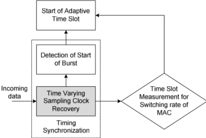
Although Direct Sequence Spread Spectrum has the advantages of security, low interference and Power Spectral Density (PSD) [4], timing synchronization is one of the major concerns of such systems. The problem of timing synchronization includes; (1) Estimation and Compensation of time varying Sampling Clock Offset (SCO) caused due to sampling clock inaccuracies and (2) Detection of the Start of burst for burst mode of transmission. Both these operations are very important in wideband networking radio operation as they directly affect the adaptive time slot algorithm in Adaptive TDMA based Medium Access Control (MAC) protocol. Figure 1 shows the flow graph of adaptive time slot algorithm in wideband networking operation and its relation with the timing synchronization.
Figure 1. Adaptive time slot algorithm and its relation with the timing synchronization (shaded block is the scope of this
paper)
The paper is organized as follows. Section 2 presents some research work related to the estimation of sampling clock offset. Section 3 presents the system overview. The problem is formulated in section 4. The proposed sampling clock recovery algorithm is presented in section 5. Simulation results and comparison of the proposed algorithm with the existing techniques is given in section 6 followed by hardware architecture in section 7. Finally, section 8 concludes the paper.
2.
Related Work
the inherent inaccuracies of transmit and receive crystal oscillators. Due to thermal drift, this sampling clock frequency offset will also change slowly in time [5]. A time domain-based sampling clock offset estimation and correction algorithm is presented in [6]. This algorithm is more specific to Orthogonal Frequency Division Multiplexing (OFDM) systems. A more generic low complexity algorithm for sampling clock offset estimation is proposed in [7]. Another algorithm for fractional timing estimation using two samples per symbol is proposed in [8]. Both the algorithms proposed in [7] and [8] have two major limitations. Firstly, they are only valid for constant drift between the transmitter and receiver sampling clocks and secondly, they do not incorporate the multipath channel effects while evaluating the estimator’s performance. An algorithm based on Sample Point Reordering (SPR) is proposed in [9] but it assumes sampling clock inaccuracies of up to only 12 ppm and the performance is affected if the amount of frequency offset present in the received signal is large. The algorithms given in [6]-[9] provide SCO estimate only and do not explain the method of proper SCO compensation for high data rate systems.
To combat multipath fading effects, especially in fast fading channels, many communication systems use burst mode of transmission [10]. The size of each burst is selected such that the channel behaves time invariant within the duration of each burst [11]. Consequently, timing and frequency synchronization, channel estimation, equalization etc. are performed on each burst independently. In such systems, sampling clock offset needs to be tracked for each burst independently. Moreover, in a multiuser system, sampling clock offset mostly changes because of frequent switching of transmitting or receiving user.
To overcome the limitations of the existing algorithms mentioned above, a complete and robust sampling clock recovery algorithm for burst mode of transmission in wideband networking radios has been proposed. The proposed Sampling clock recovery algorithm consists of three stages. In the first stage, Sampling Clock Offset (SCO) is estimated at chip level. In the second stage, the SCO estimates are post-filtered to improve the tracking performance. We present a new post-filtering method namely Steady-State State-Space Recursive Least Squares with Adaptive Memory (S4RLSWAM). For the third stage of SCO compensation, a feedforward Lagrange interpolation based algorithm is proposed. The proposed algorithm is actually part of complete wideband waveform design that has been designed, implemented and tested on SDR platform.
3.
System Overview
In wideband SDR waveforms, multiuser support is usually provided by Time Division Multiple Access (TDMA) and direct sequence spreading is used for security purpose only.
Since different applications (e.g. Push To Talk (PTT), position tracking, point-to-point calls, messages, file transfer, video communication etc.) have different Quality of Service (QoS) requirements. This varying QoS requirement is guaranteed by Adaptive TDMA (ATDMA). It provides certain end-to-end delay and reliability guarantees to different applications according to their QOS requirement. However, there is also certain delay constraint for non-real-time applications too, though not tightly bound. The real-non-real-time requirement is met in ATDMA based MAC protocol by guaranteeing the allocation of slots within the delay bound, while reliability is ensured by allocating conflict free time slots. The sampling clock recovery algorithm is very important in wideband networking radio operation as it directly affects the adaptive time slot algorithm in Adaptive TDMA based Medium Access Control (MAC) protocol (see Figure 1).
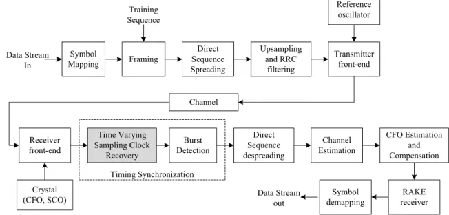
The physical layer of the wideband networking waveform based communication system is shown in Figure 2. At the transmitter side, the data stream is first mapped using QPSK symbol mapping. Bursts of the symbols are formed in which specific training sequence (to be discussed later) is inserted prior to each data burst. After direct sequence spreading, upsampling and Root Raised Cosine (RRC) filtering, the data is modulated with the carrier generated from the reference oscillator. After passing through channel, the data is received at the receiver’s front-end. The crystal oscillator of the receiving device generates Carrier Frequency Offset (CFO) and Sampling Clock Offset (SCO). The next block is the scope of this paper which is SCO estimation & compensation. This stage is very important in case of Adaptive Time Division Multiple Access (ATDMA) since it controls the time slot measurement switching rate for Medium Access Control (see Figure 1). Next block is the detection of start of burst. After the detection of each valid burst, despreading operation is performed. The next blocks including channel estimation, CFO estimation \& compensation and RAKE receiver are not the scope of this paper. However, efficient algorithms for these operations have also been proposed, implemented and tested by the authors. At the end, symbol demapping is performed to retrieve the data.
4.
Problem Formulation
The transmitted baseband wideband direct sequence signal samples prior to upsampling and pulse shaping can be expressed as
1
0
( ) ( ) ( )
M m
s
s t g mπ t mT −
=
=
∑
− (1)where M is the number of symbols used for synchronization,
International Journal of Communication Networks and Information Security (IJCNIS) Vol. 5, No. 1, April 2013
Symbol Mapping Data Stream
In
Direct Sequence Spreading
Upsampling and RRC
filtering
Framing Transmitter
front-end Reference
oscillator
Channel
Receiver front-end
Crystal (CFO, SCO)
Time Varying Sampling Clock
Recovery
Direct Sequence despreading Burst
Detection
Channel Estimation
CFO Estimation and Compensation
RAKE receiver Symbol
demapping Data Stream
out Training
Sequence
Timing Synchronization
Figure 2. Physical Layer block diagram of Wideband networking waveform (shaded block is the scope of this paper)
time span Ts, respectively. Symbol duration is denoted by Ts
such that Ts = GTc, where G is the spreading gain and Tc is
the duration of one chip of spreading waveform. The data from each user is upsampled and filtered through Root Raised Cosine (RRC) filter [12] with impulse response given as
2
sin((1 ) / ) cos((1 ) / )
4 /
( ) 4
(1 (4 / ) )
.
c c
c T
c c
R t T
R t T
Rt T
g t R
T Rt T
π π
π
−
+ +
=
−
(2) where R is the roll-off factor, T is the duration of each sample. Let the upsampled and filtered signal be x(t). After passing through multipath fading channel, the signal for each burst of data is given as [13]
1
( )
( ) ( ) ( ( )) ( )
J l
l
j t
l l
r t α t x t τ ε t e τ n t =
Ω −
=
∑
− − + (3)where J is the number of multipath, αl(t) is the fading
coefficient of lth path, τl is the path delay of lth path, Ω is the
carrier frequency offset which is present due to local oscillator frequency mismatch and/or Doppler spread, n(t) is the White Gaussian Noise with zero mean and variance σ2 and ε(t) is an unknown slowly varying time delay produced due to Sampling Clock Offset (SCO). This slowly varying time delay is produced due to frequency drift between the oscillators of the two communicating devices.
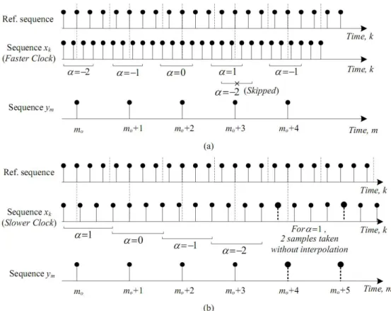
At the receiver, the analog received signal is first sampled by Analog-to-Digital Converter (ADC). The drift caused by the sampling clocks of the radios produces sampling clock errors at the ADC before timing and frequency estimation. Due to the sampling clock errors, ADC starts to sample at an unknown uncertain rate [9]. This uncertain rate is neither synchronous to the chip rate nor its oversampled rate. During the transmission of one burst, this clock error is accumulated. This causes excess and starvation of data samples at the output of ADC for slower and faster receiver sampling clocks, respectively. The situation is depicted in Figure 3.
5.
Proposed
Sampling
Clock
Recovery
Algorithm
In this section, the proposed algorithm for sampling clock recovery has been presented. A three stage clock recovery algorithm has been proposed, including:
• Estimation of slowly varying time delay
• Post filtering of the time delay estimates
• Clock offset compensation 5.1. Stage 1
The first stage of the algorithm finds the estimate of the slowly varying time delay ε(t) defined in (3). The received signal is first sampled at a sample rate of N/Tc, where N is the
upsampling factor and Tc is the chip duration. The sampled
signal is given as
( / ).
k
r =r kT N (4)
After processing through receiving matched filter (i.e. RRC filter) having impulse response of gR,k, the filtered
signal is given by
, *
k k R k
x =r g (5) where * denotes the convolution sum. Now, the unbiased estimate of sampling clock offset εˆ is found by KN samples of the filtered sequence using [14]
1
2 2 /
0
ˆ arg
2
.
KN
j k N k
k
N
x
e
πε π − − = = −
∑
(6)In (6), KN is the number of samples used for estimation. The authors of [14] estimate ε section by section by assuming very slow variation in time. For each section ∆m (where ε is
assumed to be constant), an estimate εˆm is found. This
assumption is not practical in the presence of large clock offset. In our proposed estimator, the estimate εˆm for each
incoming chip sample is found by computing the complex Fourier coefficient of the KN chips samples where K is a design constant to be discussed later. The proposed sliding window computation of the estimates is given by
1
2 2 /
ˆ arg
2
.
KN m
j k N
m k
k m
N
x
e
πε π + − − = = −
∑
(7)The sampling rate must be such that the spectral component of the filtered data at 1/Tc can be represented. It means that
we must have N/Tc > 2/Tc. So, N = 4 has been chosen.
Now, for N = 4, substitute m = 4n in (7), so that it can further be written as
1 2 2
4 3 4 1
1
1 2 2
4 4 2
2
ˆ tan
.
K m
n n
n m
m K m
n n n m
x
x
x
x
ε π + − + + − = + − + = = −
−
−
∑
∑
(8)5.2. Stage 2
The second stage of SCO estimation gives the optimal estimate ˜εm by post-filtering the estimate εˆm . The main
advantage of post-filtering is the reduction of variance of the estimates. In this paper, a new adaptive filter namely State Space Recursive Least Squares with Adaptive Memory (SSRLSWAM) has been introduced for post-filtering. SSRLSWAM has very good tracking performance especially in time-varying environments [15]. The reason for selecting SSRLSWAM instead of other adaptive filters (e.g. Least Mean Square filter, Kalman filter etc.) is the adaptive tuning of the forgetting factor, which is a key parameter in the SSRLSWAM algorithm. Since SSRLSWAM is computationally extensive, an approximate solution is used which is termed as Steady State SSRLSWAM (or S4RLSWAM). The steady state algorithm is still time varying due to the time varying behavior of the forgetting factor.
Since the SCO estimate from the first stage is bounded by
‒N/2 ≤ εˆm < N/2, the post-filtered estimate ˜εm must also be
bounded. Therefore, S4RLSWAM cannot be directly applied for the post-filtering of SCO estimates. A new idea of boundedness has been proposed within S4RLSWAM algorithm. The proposed idea is to apply modulo‒N
operation to the prediction error and a-posteriori states to reduce them to the interval [‒N/2, N/2).
Now, the summarized S4RLSWAM algorithm with the proposed modulo‒N operation ([.]N) is described which has
been used to find the optimal SCO estimate ˜εm (detailed
generic algorithm of S4RLSWAM can be found in [15]. Since it is a recursive algorithm, it needs to be initialized. The method of regularization term has been used for initialization. Following initializations can be taken to simplify the process.
ˆ [0] , [0]x
ψ =0 =0
The constant velocity model [16] has been used as the state space model of the signal. This model (unforced) is given as
[
]
1 1
, 1 0
0 1
.
A=
C=
(9)The algorithm then proceeds as follows.
• Predicted (a-priori) states 1 ˆ
m m
x = Ax −
• Predicted output (Predicted SCO Estimate)
m Cxm
ε =
• Prediction error (
ε
ˆ
mis the input to filter)[
ˆ]
m m m N
ξ = ε −ε • Forgetting factor update
1 1
T T
m m m A C m
λ λ λ =
λ − +αψ − ξ
+−• Calculation of matrices Pm and Sm
2 2
2 3
1 (1 )
(1 ) (1 ) /
m m
m
m m m
P Pλ λ λ
λ λ λ
− − = = − −
2 22 2(1 )
2(1 ) (1 ) ( 1 2 ) /
m m
m
m m m m
P
S Sλ λ λ λ
λ λ λ λ
λ − − − ∂ = = = − − − − − ∂
• Calculation of S4RLSWAM gain
1 1 1 1 1 1
T T
m m m
T T
m m
K AP A C
CAP A C
λ λ − − − − − = × +
• States (a-posteriori) estimates ˆm
[
ˆm 1]
m m N
x = Ax − +K ξ
• Output estimate (Optimal SCO estimate
˜
ε
m)ˆ
m Cxm
ε% = • Update ψm
ψm =
(
A−K CAm)
ψm−1+S Cm Tξm5.3. Stage 3
International Journal of Communication Networks and Information Security (IJCNIS) Vol. 5, No. 1, April 2013
Figure 4. Proposed concept of SCO compensation using cubic interpolation; (a) Faster sampling clock (b) Slower sampling clock (Rapid changes in the integer part α are shown to explain all the cases; this variation is slow in practical systems) mentioned in the previous section that there can be both
slower and faster receiver sampling clocks in different devices resulting in positive and negative clock drifts respectively (Figure 3). The situation is further depicted in Figure 4, which shows the method of selection of samples to be interpolated based on the estimated sampling clock offset.
From (8) it can be seen that the possible range of εˆm is ‒2 ≤ εˆm < 2 (for N = 4), which will be the same for ˜εm. Let the
integer part and fractional parts of ε ˜m be α and δ respectively.
If i is an index incremented by N for each value of m, then for
N = 4, the samples for cubic interpolation are given as
1 1
2
3 1
4 2
.
i i i i
s x
s x
s x
s x
α
α
α
α + −
+
+ +
+ + =
= = =
After selecting the samples for interpolation, the fractional part δ is used to perform the Lagrange polynomial based cubic interpolation. Let s1, s2, s3, and s4 be the 4 samples of the filtered signal corresponding to a specific value of m on which cubic interpolation is to be performed. For each estimate ˜εm, the fractional part δm is used to interpolate the 4
samples. The compensated and downsampled sample ym is
given as
3 3
1 2 4
2 3 1
2
1 2 4
3 2
6 2 2 6
2 2
3 2 6
m m
m
m
s
s s s
y
s s
s
s s s
s s
δ
δ
δ
= − + − +
+ − +
+ − − + − +
(10)
Another problem caused by the sampling clock drift is the excess and starvation of samples at the receiver due to faster and slower receiver sampling clocks respectively. In case of faster receiver clock, samples must be discarded whereas in case of slower receiver clock, extra samples must be put to avoid starvation of data samples.
A new technique to avoid starvation or excess of samples is proposed. The proposed technique works as follows (assuming N = 4). The integer part α of the SCO estimate decides whether the downsampler has to put required samples or discard extra samples. This is explained in Figure 4, which shows that if the receiver has faster sampling clock, the integer part α increases from ‒2 to 1 slowly. Since SCO estimate has an upper bound of ˜εm < 2 integer part jumps
from 1 to ‒2. At this point a sample is discarded for the purpose of synchronization. Similarly, if the receiver has slower sampling clock, the integer part α decreases from 1 to
6.
Simulation Results
In this section, simulation results of the proposed sampling clock recovery algorithm have been presented. The parameters used in the simulation are as follows.
• Number of modulated symbols in each (Nspr) = 288 • RRC roll-off factor (R) = 0.65
• Number of samples used for SCO estimation (K) = 32
• Initial value of forgetting factor (λinit) = 0.995 • Constant α = 0.000005
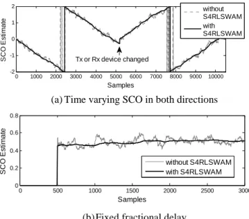
Golay sequences of length 16 have been used for spreading and QPSK has been used as the modulation technique. Figure 5 shows the tracking performance of the proposed estimator with and without S4RLSWAM post-filtering at SNR of 2 dB. S4RLSWAM has been initialized by the method of regularization term. The performance metric used in Figure 5 is the post-filtered SCO estimate ˜εm.
In Figure 5(a), tracking performance is shown for a slowly varying time delay due to clock offsets of ‒200 ppm and +200 ppm. The sudden change of clock offset is common in communication networks due to the change of transmitting or receiving device. It can be seen that the proposed estimator efficiently tracks the varying time delay even after the sudden change in clock offset. The proposed estimator can cope with large sampling clock offsets in contrast to the algorithm given in [11] which assumes the inaccuracy of oscillators up to only 12 ppm. Figure 5(b) shows the tracking performance of the proposed estimator for a fixed fractional time delay of 0.5T. It can be seen that the proposed estimator performs well for both the fixed and varying time delays.
0 1000 2000 3000 4000 5000 6000 7000 8000 9000 10000 -2
-1 0 1 2
Samples
S
C
O
E
s
ti
m
a
te
without S4RLSWAM with S4RLSWAM
Tx or Rx device changed
(a)Time varying SCO in both directions
0 500 1000 1500 2000 2500 3000
0 0.2 0.4 0.6 0.8
Samples
S
C
O
E
s
ti
m
a
te
without S4RLSWAM with S4RLSWAM
(b)Fixed fractional delay
Figure 5. Performance of the proposed SCO estimator for time varying and fixed clock offsets
The comparison of variances of the proposed and other well-known SCO estimators is shown in Figure 6. The performance metric (i.e. estimator’s variance) is given as
(
)
21
1
var( ) ( )
M
i i
E M
ε ε ε
=
=
∑
− )% % % (11)
where
1
1 ( )
M
i i
E M
ε ε
=
=
∑
)
% % (12)
is the sample mean of the post-filtered estimate ˜εm and M is
the number of realizations. In this simulation, we have taken
M = 2000. For comparison, ML-based algorithm [17],
Montazeri \& Kiasaleh's estimator [7] and a two samples/symbol based feedforward algorithm given in [8] have been considered. It can be seen that the proposed estimator shows considerable performance improvement when compared to other estimators at all SNRs. It is also worth mentioning here that the algorithms given in [7] and [8] are applicable only when the time delay is fixed i.e. ε(t) = ε, whereas the proposed estimator is capable of estimating both the fixed and time varying delays efficiently.
0 5 10 15 20 25 30 35
10-7 10-6 10-5 10-4 10-3 10-2 10-1
Eb/N0 (dB)
v
a
ri
a
n
c
e
ML-based Algorithm
Montazeri & Kiasaleh Algorithm [16] Two Samples/Symbol Algorithm [17] Proposed Algorithm
Figure 6. Performance comparison of the proposed estimator with other well-known estimators
Now, we present the Bit Error Rate (BER) performance of the overall all system using the proposed timing synchronization approach. In Figure 7, the Bit Error Rate (BER) performance in AWGN and Stanford University Interim-3 (SUI-3) channel model [18] with and without sampling clock errors is shown. It can be seen that the BER performance of the system with proposed timing synchronization is robust against the sampling clock errors even at low SNRs and in the presence of multipath fading effects.
0 1 2 3 4 5 6 7
10-6 10-5 10-4 10-3 10-2 10-1 100
E b/N0 (dB)
B
E
R
SUI-3 with SCO SUI-3 without SCO AWGN with SCO AWGN without SCO
International Journal of Communication Networks and Information Security (IJCNIS) Vol. 5, No. 1, April 2013
1
en
2
en
3
en
4
en
1
en
1
en
1
en
1
en
2
| |
2
| |
2
| |
2
| | k
r
m
y
clk
1
en
2
en
3
en
4
en
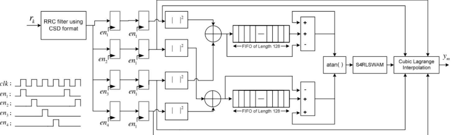
Figure 8. Proposed FPGA implementation of the proposed sampling clock recovery algorithm
7.
Efficient FPGA Implementation
In this section, the hardware architectures of the proposed sampling clock recovery and burst detection algorithms for FPGA implementation on SDR platform have been presented. The FPGA device used for the implementation is XC3SD3400A which belongs to the Spartan-3A DSP family of FPGAs. This family of FPGA offers density of 3.4million system gates. The Spartan-3A DSP family builds on the success of the Spartan-3A FPGA family by adding XtremeDSP™ DSP48A slices. New features improve system performance and reduce the cost of configuration. These Spartan-3A DSP FPGA enhancements, combined with proven 90 nm process technology, deliver more functionality and bandwidth per dollar than ever before, setting the new standard in the programmable logic and DSP processing industry.
Figure 8 shows the hardware architecture for sampling clock recovery algorithm. First of all, multiplier-less RRC filter of order 16 has been implemented using Canonic Signed Digit (CSD) representation of filter coefficients [19]. After filtering, a high data rate parallel processing based realization of (7) and (8) for the estimation of each incoming sample has been presented. This high data rate parallel processing is specific to the case when N = 4. A similar approach can be followed for higher values of N, but it will certainly increase the complexity of the system. The four enable signals used in the realization are also shown in Figure 8. After squaring and summation, the sliding window computation of (8) has been implemented by the use of two First-Input First-Output (FIFOs). The inphase and quadrature components are then fed to atan() block which is implemented using the CORDIC core of Xilinx core generator. The resulting SCO estimate then goes to S4RLSWAM block for post-filtering. The block-level architecture of implemented S4RLSWAM has been shown in Figure 9. Finally, the proposed cubic Lagrange interpolation is implemented which takes the post-filtered SCO estimate and the corresponding four samples to perform the cubic interpolation for SCO compensation. The device utilization summary of the FPGA implementation is shown in Table 1.
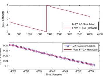
Tracking performance of the proposed SCO estimator (for negative offset) captured from ChipScope after implementation on FPGA is shown in Figure 10. The input data is taken at an SNR = ‒2. It is obvious that the estimate
has very low variance. The transition occurs from ‒32766 to 32762 (i.e. from ‒1.9999 to 1.996 for Q2.14 format), which is almost equal to that of simulated result. This is further elaborated in Figure 11 which shows the comparison of SCO estimate obtained from MATLAB simulation and FPGA hardware. It can be seen that both the estimates are identical since they are overlapping each other. The bottom sub-figure shows the magnified SCO estimate of the last few samples from the first figure to have a clear visualization.
1, 1 ˆm
x −
2, 1 ˆ m
x −
m
ε%
m
λ
1
m
λ −
1,m
ψ
2,m ψ
m
ξ εˆm
−
−
+
Figure 9. Block level architecture for S4RLSWAM implementation on FPGA
Figure 10. Performance of implemented SCO estimator on FPGA (captured from ChipScope)
0 500 1000 1500 2000 2500 3000 3500 4000 4500
-2 -1 0 1 2
S
C
O
E
s
ti
m
a
te
4025 4030 4035 4040 4045 4050 4055
0.2 0.21 0.22 0.23 0.24
Time Samples
S
C
O
E
s
ti
m
a
te
MATLAB Simulation From FPGA Hardware MATLAB Simulation From FPGA Hardware
Figure 11. Comparison of MATLAB simulation and FPGA hardware results of the proposed SCO estimator
Table 1. Device Utilization Summary
Resources Used Total Percentage
Number of Slices 4076 23872 17%
Number of Slice Flip Flops 5002 47744 9%
Number of 4 input LUTs 5585 47744 11%
Number of BRAMs 14 126 11%
Number of DSP48s 47 126 37%
8.
Conclusion and Future Work
In this paper, practically efficient algorithm for sampling clock recovery for burst mode wideband networking waveform of software defined radio has been proposed. Sampling clock recovery plays a key role in the adaptive time slot measurement for switching rate of medium access control. The proposed sampling clock recovery algorithm includes proposed modified square timing estimation, S4RLSWAM based post-filtering and proposed cubic interpolation based compensation. The proposed algorithm shows considerable performance improvement when compared to other well-known algorithms. Our simulation has also shown that the proposed estimator is capable of estimating both the fixed and time varying delays. Practical FPGA architectures and implementation results for the proposed algorithm on FPGA platform have also been
presented. It has been shown that the hardware results are identical to the simulation results.
Some other post-filtering approaches can be applied to the proposed SCO estimation as future research work. Moreover, the FPGA implementation can be further optimized to achieve lesser resource utilization.
References
[1] J. Rohde, and T. S. Toftegaard, “Adaptive cognitive radio technology for low power wireless personal area network devices”, Wireless Personal Communications, Vol. 58, No. 1, pp. 111-123, 2011.
[2] S. Han, J-H. Park, H-H. Shin, and B-S. Kim, “Performance enhancements in TDMA-based tactical wireless networks”, in Proceedings of Vehicular
Technology Conference, Vol. 1, pp. 1-5, 2012.
[3] M. Nakagawa, “Consumer communications based on spread spectrum technologies”, in Proceedings of
IEEE 3rd International Symposium on Spread Spectrum Techniques and Applications, Vol. 1, pp.
138-145, 1994.
[4] A. J. Viterbi, CDMA: Principles of Spread Spectrum
Communication, Addison-Wesley, 1995.
[5] E. Grass, K. Tittelbach-Helmrich, U. Jagdhold, A. Troya, G. Lippert, et al., “On the Single-Chip Implementation of a Hiperlan/2 and IEEE 802.11a Capable Modem”, IEEE Personal Communications, Vol. 8, No. 6, pp. 48-57, 2001.
[6] B. Ai, Y. Shen, Z. D. Zhong, and B. H. Zhang, “Enhanced sampling clock offset correction based on time domain estimation scheme, IEEE Transactions
on Consumer Electronics, Vol. 57, No. 2, pp.
696-704, 2011.
[7] A. Montazeri, K. Kiasaleh, “Design and performance analysis of a low complexity digital clock recovery algorithm for software defined radio applications”,
IEEE Transactions on Consumer Electronics, Vol. 56,
No. 3, pp. 1258-1263, 2010.
[8] W-P. Zhu, Y. Yan, M. O. Ahmed, and M. N. S. Swamy, “Feedforward symbol timing recovery technique using two samples per symbol”, IEEE
Transactions on Circuits and Systems-I, Vol. 52, No.
11, pp. 2490-2500, 2005.
[9] C-F. Li, Y-S. Chu, J-S. Ho, and W-H. Sheen, “Cell search in WCDMA under large-frequency and clock errors: Algorithm to hardware implementation”, IEEE
Transactions on Circuits and Systems-I, Vol. 55, No.
2, pp. 659-671, 2008.
[10] U. Mengali, M. Morelli, “Data-aided frequency estimation for burst digital transmission”, IEEE
Transactions on Communications, Vol. 45, No. 1, pp.
23-25, 1997.
[11] A. Goldsmith, Wireless Communications, Cambridge University Press, UK, 2005.
[12] B. Sklar, Digital Communications; Fundamentals and
Applications, 2nd Ed., Prentice Hall, 2002.
[13] K. Fazel, and S. Kaiser, Multicarrier and Spread
Spectrum Systems, John Wiley and Sons, 2003.
International Journal of Communication Networks and Information Security (IJCNIS) Vol. 5, No. 1, April 2013 [15] M. B. Malik, “State-space recursive least squares with
adaptive memory”, Signal Processing Journal, Vol. 86, pp. 1365-1374, 2006.
[16] Y. Bar-Shalom, and X-R. Li, and T. Kirubarajan,
Estimation with Applications to Tracking and Navigation, New York, Wiley, 2001.
[17] U. Mengali, and A. N. D’Andrea, Synchronization
Techniques for Digital Receivers, New York, Plenum
Press, 1997.
[18] IEEE 802.16 Broadband Wireless Access Working Group, Channel models for fixed wireless applications, http://www.ieee802.org/16/tg3/contrib. [Accessed on 10 Dec. 2009].
[19] S. A. Khan, Digital Design for Signal Processing
Systems: A Practical Approach, 1st Ed., John Wiley
and Sons, 2011.