D
2.5-V Virtual Ground for 5-V/GND Analog
Systems
D
High Output-Current Capability
Sink or Source . . . 20 mA Typ
D
Micropower Operation . . . 170
µ
A Typ
D
Excellent Regulation Characteristics
– Output Regulation
– 45
µ
V Typ at I
O= 0 to – 10 mA
+15
µ
V Typ at I
O= 0 to + 10 mA
– Input Regulation = 1.5
µ
V/V Typ
D
Low-Impedance Output . . . 0.0075
Ω
Typ
D
Macromodel Included
description
In signal-conditioning applications using a single
power source, a reference voltage is required for
termination of all signal grounds. To accomplish
this, engineers have typically used solutions
consisting of resistors, capacitors, operational
amplifiers, and voltage references. Texas
Instru-ments has eliminated all of those components
with one easy-to-use 3-terminal device. That
device is the TLE2425 precision virtual ground.
Use of the TLE2425 over other typical circuit
solutions gives the designer increased dynamic
signal range, improved signal-to-noise ratio,
lower distortion, improved signal accuracy, and
easier interfacing to ADCs and DACs. These
benefits are the result of combining a precision
micropower voltage reference and a
high-perfor-mance precision operational amplifier in a single
silicon chip. It is the precision and performance of
these two circuit functions together that yield such
dramatic system-level performance.
The TLE2425 improves input regulation as well as output regulation and, in addition, reduces output impedance
and power dissipation in a majority of virtual-ground-generation circuits. Both input regulation and load
regulation exceed 12 bits of accuracy on a single 5-V system. Signal-conditioning front ends of data acquisition
systems that push 12 bits and beyond can use the TLE2425 to eliminate a major source of system error.
AVAILABLE OPTIONS TA SMALL OUTLINE(D) PLASTIC TO-226AA (LP) 0°C to 70°C TLE2425CD TLE2425CD – 40°C to 85°C TLE2425ID TLE2425ID – 55°C to 125°C TLE2425MD — † The D package is available taped and reeled. Add R suffix to
the device type (e.g., TLE2425CDR).
Please be aware that an important notice concerning availability, standard warranty, and use in critical applications of Texas Instruments semiconductor products and disclaimers thereto appears at the end of this data sheet.
V) – Output V oltage Change – µ V 80 – 20 0 20 60 40 – 40 – 60 – 80 – 100 10 8 – 2 0 2 4 6 – 4 – 6 – 8 – 10 100 OUTPUT REGULATION IO – Output Current – mA VI = 5 V TA = – 55°C TA = 25°C TA = 125°C ∆ VO TA = – 40°C TA = 125°C TA = – 55°C TA = 0°C TA = 25°C
1 2 3 4 8 7 6 5 OUT COMMON IN NC NC NC NC NC D, OR JG PACKAGE (TOP VIEW) NC – No internal connection OUT IN COMMON LP PACKAGE (TOP VIEW)
absolute maximum ratings over operating free-air temperature range (unless otherwise noted)
†
Continuous input voltage, V
I. . .
40 V
Output current, I
O. . .
±
80 mA
Duration of short-circuit current at (or below) 25
°
C (see Note 1)
. . .
unlimited
Continuous total power dissipation
. . .
See Dissipation Rating Table
Operating free-air temperature range, T
A: C-suffix 0
. . .
°
C to 70
°
C
I-suffix
. . .
–40
°
C to 85
°
C
M-suffix
. . .
–55
°
C to 125
°
C
Storage temperature range, T
stg. . .
–65
°
C to 150
°
C
Lead temperature 1,6 mm (1/16 inch) from case for 10 seconds: D package
. . .
260
°
C
Lead temperature 1,6 mm (1/16 inch) from case for 60 seconds: JG or LP package
. . .
300
°
C
† Stresses beyond those listed under “absolute maximum ratings” may cause permanent damage to the device. These are stress ratings only, and functional operation of the device at these or any other conditions beyond those indicated under “recommended operating conditions” is not implied. Exposure to absolute-maximum-rated conditions for extended periods may affect device reliability.NOTE 1: The output may be shorted to either supply. Temperature and/or supply voltages must be limited to ensure that the maximum dissipation rating is not exceeded.
DISSIPATION RATING TABLE
PACKAGE TA ≤ 25°C DERATING FACTOR TA = 70°C TA = 85°C TA = 125°C
PACKAGE POWER RATING
ABOVE TA = 25°C POWER RATING POWER RATING POWER RATING
D 725 mV 5.8 mW/°C 464 mW 377 mW 145 mW
JG 1050 mV 8.4 mW/°C 672 mW 546 mW 210 mW
LP 775 mV 6.2 mW/°C 496 mW 403 mW 155 mW
recommended operating conditions
C-SUFFIX I-SUFFIX M-SUFFIX
UNIT
MIN MAX MIN MAX MIN MAX UNIT
Input voltage, VI 4 40 4 40 4 40 V
electrical characteristics at specified free-air temperature, V
I
= 5 V, I
O
= 0 (unless otherwise noted)
PARAMETER TEST CONDITIONS TA† TLE2425C UNIT
PARAMETER TEST CONDITIONS TA†
MIN TYP MAX UNIT
Output voltage 25°C 2.48 2.5 2.52 V
Output voltage
Full range 2.47 2.53 V
Temperature coefficient of output voltage 25°C 20 ppm/°C
Bias current IO = 0 25°C 170 250 µA
Bias current IO = 0
Full range 250 µA
VI = 4 5 V to 5 5 V 25°C 1.5 20 µV
Input voltage regulation
VI = 4.5 V to 5.5 V
Full range 25 µV
Input voltage regulation
VI = 4 V to 40 V 25°C 1.5 20 µV/V
VI = 4 V to 40 V
Full range 25 µV/V
Ripple rejection f = 120 Hz, ∆VI(PP) = 1 V 25°C 80 dB
‡ IO = 0 to 10 mA
25°C – 160 – 45 160 Output voltage regulation (source current)‡g g ( ) IO = 0 to – 10 mA Full range – 250 250 µV
IO = 0 to – 20 mA 25°C – 450 – 150 450
‡ IO = 0 to 10 mA
25°C – 160 15 160
Output voltage regulation (sink current)‡g g ( ) IO = 0 to 10 mA Full range – 250 250 µV
IO = 0 to 20 mA 25°C – 235 65 235
Long-term drift of output voltage ∆t = 1000 h, Noncumulative 25°C 15 ppm
Output impedance 25°C 7.5 22.5 mΩ
Short-circuit output current (sink current) VO = 5 V
25°C 30 55 mA
Short-circuit output current (source current) VO = 0 25°C – 30 – 50 mA
Output noise voltage, rms f = 10 Hz to 10 kHz 25°C 100 µV
VO to 0.1%, CL = 0 110
Output voltage response to output current step
O ,
IO = ±10 mA CL = 100 pF
25°C 115 µs
Output voltage response to output current step
VO to 0.01%, CL = 0
25°C
180 µs
O ,
IO = ±10 mA CL = 100 pF 180
Output voltage response to input voltage step VI = 4.5 to 5.5 V, VO to 0.1% 25°C 12 µs Output voltage response to input voltage step
VI = 4.5 to 5.5 V, VO to 0.01% 25°C 30 µs
Output voltage turn on response VI = 0 to 5 V, VO to 0.1% 25°C 125 µs
Output voltage turn-on response
VI = 0 to 5 V, VO to 0.01% 25°C 210 µs
† Full range is 0°C to 70°C.
electrical characteristics at specified free-air temperature, V
I
= 5 V, I
O
= 0 (unless otherwise noted)
PARAMETER TEST CONDITIONS TA† TLE2425I UNIT
PARAMETER TEST CONDITIONS TA†
MIN TYP MAX UNIT
Output voltage 25°C 2.48 2.5 2.52 V
Output voltage
Full range 2.47 2.53 V
Temperature coefficient of output voltage 25°C 20 ppm/°C
Bias current IO = 0 25°C 170 250 µA
Bias current IO = 0
Full range 250 µA
VI = 4 5 V to 5 5 V 25°C 1.5 20 µV
Input voltage regulation
VI = 4.5 V to 5.5 V
Full range 75 µV
Input voltage regulation
VI = 4 V to 40 V 25°C 1.5 20 µV/V
VI = 4 V to 40 V
Full range 75 µV/V
Ripple rejection f = 120 Hz, ∆VI(PP) = 1 V 25°C 80 dB
‡ IO = 0 to 10 mA
25°C – 160 – 45 160 Output voltage regulation (source current)‡g g ( ) IO = 0 to – 10 mA Full range – 250 250 µV
IO = 0 to – 20 mA 25°C – 450 – 150 450
‡ IO = 0 to 8 mA
25°C – 160 15 160
Output voltage regulation (sink current)‡g g ( ) IO = 0 to 8 mA Full range – 250 250 µV
IO = 0 to 20 mA 25°C – 235 65 235
Long-term drift of output voltage ∆t = 1000 h, Noncumulative 25°C 15 ppm
Output impedance 25°C 7.5 22.5 mΩ
Short-circuit output current (sink current) VO = 5 V
25°C 30 55 mA
Short-circuit output current (source current) VO = 0 25°C – 30 – 50 mA
Output noise voltage, rms f = 10 Hz to 10 kHz 25°C 100 µV
VO to 0.1%, CL = 0 110
Output voltage response to output current step
O ,
IO = ±10 mA CL = 100 pF
25°C 115 µs
Output voltage response to output current step
VO to 0.01%, CL = 0
25°C
180 µs
O ,
IO = ±10 mA CL = 100 pF 180
Output voltage response to input voltage step VI = 4.5 to 5.5 V, VO to 0.1% 25°C 12 µs Output voltage response to input voltage step
VI = 4.5 to 5.5 V, VO to 0.01% 25°C 30 µs
Output voltage turn on response VI = 0 to 5 V, VO to 0.1% 25°C 125 µs
Output voltage turn-on response
VI = 0 to 5 V, VO to 0.01% 25°C 210 µs
† Full range is – 40°C to 85°C.
electrical characteristics at specified free-air temperature, V
I
= 5 V, I
O
= 0 (unless otherwise noted)
PARAMETER TEST CONDITIONS TA† TLE2425M UNIT
PARAMETER TEST CONDITIONS TA†
MIN TYP MAX UNIT
Output voltage 25°C 2.48 2.5 2.52 V
Output voltage
Full range 2.47 2.53 V
Temperature coefficient of output voltage 25°C 20 ppm/°C
Bias current IO = 0 25°C 170 250 µA
Bias current IO = 0
Full range 250 µA
VI = 4 5 V to 5 5 V 25°C 1.5 20 µV
Input voltage regulation
VI = 4.5 V to 5.5 V
Full range 100 µV
Input voltage regulation
VI = 4 5 V to 40 V 25°C 1.5 20 µV/V
VI = 4.5 V to 40 V
Full range 100 µV/V
Ripple rejection f = 120 Hz, ∆VI(PP) = 1 V 25°C 80 dB
‡ IO = 0 to 10 mA
25°C – 160 – 45 160 Output voltage regulation (source current)‡g g ( ) IO = 0 to – 10 mA Full range – 250 250 µV
IO = 0 to – 20 mA 25°C – 450 – 150 450
‡ IO = 0 to 3 mA
25°C – 160 15 160
Output voltage regulation (sink current)‡g g ( ) IO = 0 to 3 mA Full range – 250 250 µV
IO = 0 to 20 mA 25°C – 235 65 235
Long-term drift of output voltage ∆t = 1000 h, Noncumulative 25°C 15 ppm
Output impedance 25°C 7.5 22.5 mΩ
Short-circuit output current (sink current) VO = 5 V
25°C 30 55 mA
Short-circuit output current (source current) VO = 0 25°C – 30 – 50 mA
Output noise voltage, rms f = 10 Hz to 10 kHz 25°C 100 µV
VO to 0.1%, CL = 0 110
Output voltage response to output current step
O ,
IO = ±10 mA CL = 100 pF
25°C 115 µs
Output voltage response to output current step
VO to 0.01%, CL = 0
25°C
180 µs
O ,
IO = ±10 mA CL = 100 pF 180
Output voltage response to input voltage step VI = 4.5 to 5.5 V, VO to 0.1% 25°C 12 µs Output voltage response to input voltage step
VI = 4.5 to 5.5 V, VO to 0.01% 25°C 30 µs
Output voltage turn on response VI = 0 to 5 V, VO to 0.1% 25°C 125 µs
Output voltage turn-on response
VI = 0 to 5 V, VO to 0.01% 25°C 210 µs
† Full range is – 55°C to 125°C.
TYPICAL CHARACTERISTICS
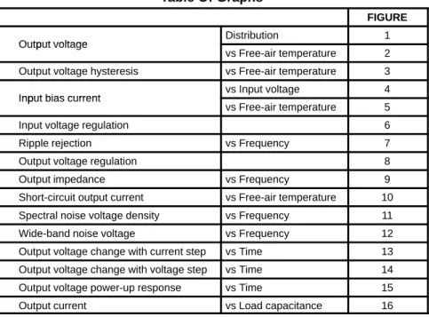
Table Of Graphs
FIGURE
Output voltage Distribution 1
Output voltage
vs Free-air temperature 2 Output voltage hysteresis vs Free-air temperature 3
Input bias current vs Input voltage 4
Input bias current
vs Free-air temperature 5
Input voltage regulation 6
Ripple rejection vs Frequency 7
Output voltage regulation 8
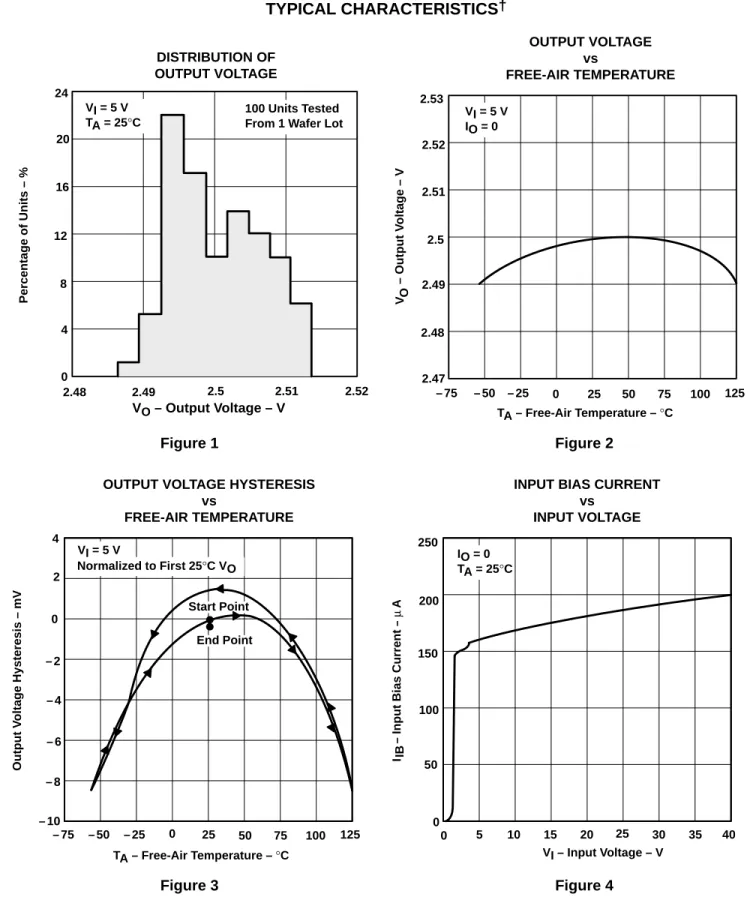
Output impedance vs Frequency 9
Short-circuit output current vs Free-air temperature 10
Spectral noise voltage density vs Frequency 11
Wide-band noise voltage vs Frequency 12
Output voltage change with current step vs Time 13 Output voltage change with voltage step vs Time 14
Output voltage power-up response vs Time 15
TYPICAL CHARACTERISTICS
†
2.48 2.49 2.5 2.51 2.52 2.47 2.53 25 50 75 100 125 0 – 25 – 50 – 75 OUTPUT VOLTAGE vs FREE-AIR TEMPERATURE 24 12 0 2.48 2.49 2.5 2.51 2.52 DISTRIBUTION OF OUTPUT VOLTAGE Percentage of Units – % VO – Output Voltage – V V) – Output V oltage – V VO TA – Free-Air Temperature – °C 20 16 8 4 VI = 5 V TA = 25°C 100 Units TestedFrom 1 Wafer Lot VI = 5 VIO = 0
Figure 1
Figure 2
200 50 0 250 150 100 5 0 10 15 20 25 30 35 40INPUT BIAS CURRENT vs
INPUT VOLTAGE OUTPUT VOLTAGE HYSTERESIS
vs FREE-AIR TEMPERATURE 2 4 0 – 2 – 4 – 6 – 10 – 8 25 50 75 100 125 0 – 25 – 50 – 75 TA – Free-Air Temperature – °C Output V oltage Hysteresis – mV VI – Input Voltage – V End Point Start Point Normalized to First 25°C VO VI = 5 V IO = 0 TA = 25°C IIB –
Input Bias Current
–
I IB
A
µ
Figure 3
Figure 4
TYPICAL CHARACTERISTICS
†
40 20 30 10 0 40 20 80 60 – 20 0 IO = 0 TA = 25°CINPUT VOLTAGE REGULATION
25 50 75 100 125 0 – 25 – 50 – 75 150 152 154 156 158 160 162 164 166 168 170 172
INPUT BIAS CURRENT vs FREE-AIR TEMPERATURE V) – Output V oltage Change – VI – Input Voltage – V TA – Free-Air Temperature – °C VO ∆ µ V VI = 5 V IO = 0 IIB –
Input Bias Current
– I IB A µ
Figure 5
Figure 6
1 k 10 k 100 k 1 M 100 10 50 90 80 60 40 70 30 20 10 RIPPLE REJECTION vs FREQUENCY Ripple Rejection – dB f – Frequency – Hz V) – Output V oltage Change – µ V 80 – 20 0 20 60 40 – 40 – 60 – 80 – 100 10 8 – 2 0 2 4 6 – 4 – 6 – 8 – 10 100OUTPUT VOLTAGE REGULATION
IO – Output Current – mA VI = 5 V TA = 125°C ∆ VO TA = 125°C TA = – 55°C TA = 0°C TA = 25°C TA = – 40°C TA = – 55°C TA = 25°C VI = 5 V ∆VI(PP) = 1 V IO = 0 TA = 25°C
Figure 7
Figure 8
TYPICAL CHARACTERISTICS
56 54 52 50 48 46 44 42 40 25 50 75 100 125 0 – 25 – 50 – 75SHORT-CIRCUIT OUTPUT CURRENT vs
FREE-AIR TEMPERATURE
IOS
–
Short-Circuit Output Current
– mA I OS TA – Free-Air Temperature – °C IOS Output Sink, VO = 5 V – IOS Output Source, VO = 0 VI = 5 V 0.1 0.01 0.001 1 k 10 k 100 k 1 M 100 100 10 10 1 OUTPUT IMPEDANCE vs FREQUENCY f – Frequency – Hz – Output Impedance – Ω zo VI = 5 V TA = 25°C IO = 0 IO = – 10 mA IO = 10 mA
Figure 9
Figure 10
100 kWIDE-BAND NOISE VOLTAGE vs FREQUENCY f – Frequency – Hz VI = 5 V TA = 25°C 1 Hz to Frequency Indicated 1 Pole Low Pass
2 Pole Low Pass 80 60 40 70 30 20 10 50 0 10 100 1 k 10 k 10 100 1 k 10 k 100 k 1400
SPECTRAL NOISE VOLTAGE DENSITY vs FREQUENCY f – Frequency – Hz 1200 1000 800 600 400 200 0 1 VI = 5 V TA = 25°C W ide-Band Noise V oltage – V rms µ V – Spectral Noise V oltage Density – Vn nV/ Hz
Figure 11
Figure 12
TYPICAL CHARACTERISTICS
OUTPUT VOLTAGE RESPONSE TO INPUT VOLTAGE STEP
vs TIME – Change In Output V oltage – mV ∆ VO t – Time - ms 500 – 500 4 0 3 2 1 – 1 – 2 – 3 – 4 0 50 100 150 200 IO = 0 CL = 100 pF TA = 25°C VO Response VI = 5.5 V VI Step VI = 4.5 V 0.1 % 0.01 % 0.1 % VI = 4.5 V 300 450 600 750 900 1050 – 1.5 V 3 2 1 – 1 – 2 – 3 – 4 4 0 1.5 V 150 0
OUTPUT VOLTAGE RESPONSE TO OUTPUT CURRENT STEP
vs TIME – Change In Output V oltage – mV ∆ VO t – Time – ms 0.1 % 0.1 % 0.01 % 0.01 % VI = 5 V CL = 100 pF TA = 25°C VO Response 10 mA IO Step 0 – 10 mA
Figure 13
Figure 14
10 – 6 – 20 5 0 – 10 – 15 – 5 20 10 15 STABILITY RANGE OUTPUT CURRENT vs LOAD CAPACITANCE I O – Output Current – mA CL– Load Capacitance – mF VI = 5 V TA = 25°C Unstable Stable 10 – 5 10 – 4 10 – 3 10 – 2 10 – 1 10 0 10 1 10 2OUTPUT VOLTAGE POWER-UP RESPONSE vs TIME V) – Output V oltage – V VO t – Time - ms IO = 0 CL = 100 pF TA = 25°C 0.1 %
Input Voltage Step
Output Voltage Response 3 2 1 0 5 0 0 10 20 130
Figure 15
Figure 16
macromodel information
* TLE2425 OPERATIONAL AMPLIFIER “MACROMODEL” SUBCIRCUIT * CREATED USING PARTS RELEASE 4.03 ON 08/21/90 AT 13:51 * REV (N/A) SUPPLY VOLTAGE: 5 V
* CONNECTIONS: INPUT * | COMMON * | | OUTPUT * | | | .SUBCKT TLE2425 3 4 5 * * OPAMP SECTION C1 11 12 21.66E – 12 C2 6 7 30.00E – 12 C3 87 0 10.64E – 9 CPSR 85 86 15.9E – 9 DCM+ 81 82 DX DCM– 83 81 DX DC 5 53 DX DE 54 5 DX DLN 92 90 DX DLP 90 91 DX DP 4 3 DX ECMR 84 99 (2,99) 1 EGND 99 0 POLY(2) (3,0) (4,0) 0 .5 .5
EPSR 85 0 POLY(1) (3,4) –16.22E–6 3.24E–6 ENSE 89 2 POLY(1) (88,0) 120E–6 1
FB 7 99 POLY(6) VB VC VE VLP VLN VPSR O 74.8E6 –10E6 10E6 10E6 + –10E6 74E6 GA 6 0 11 12 320.4E–6 GCM 0 6 10 99 1.013E–9 GPSR 85 86 (85,86) 100E–6 GRC1 4 11 (4,11) 3.204E–4 GRC2 4 12 (4,12) 3.204E–4 GRE1 13 10 (13,10) 1.038E–3 GRE2 14 10 (14,10) 1.038E–3 HLIM 90 0 VLIM 1K
HCMR 80 1 POLY(2) VCM+ VCM– 0 1E2 1E2
IRP 3 4 146E–6 IEE 3 10 DC 24.05E–6 IIO 2 0 .2E–9 I1 88 0 1E–21 Q1 11 89 13 QX Q2 12 80 14 QX R2 6 9 100.0E3 RCM 84 81 1K REE 10 99 8.316E6 RN1 87 0 2.55E8 RN2 87 88 11.67E3
macromodel information (continued)
RO1 8 5 63 RO2 7 99 62 VCM+ 82 99 1.0 VCM– 83 99 –2.3 VB 9 0 DC 0 VC 3 53 DC 1.400 VE 54 4 DC 1.400 VLIM 7 8 DC 0 VLP 91 0 DC 30 VLN 0 92 DC 30 VPSR 0 86 DC 0 RFB 5 2 1K RIN 30 1 1K RCOM 34 4 .1 *REGULATOR SECTION RG1 30 0 20MEG RG2 30 31 .2 RG3 31 35 400K RG4 35 34 411K RG5 31 36 25MEGHREG 31 32 POLY(2) VPSET VNSET 0 1E2 1E2 VREG 32 33 DC 0V
EREG 33 34 POLY(1) (36,34) 1.23 1 VADJ 36 34 1.27V
HPSET 37 0 VREG 1.030E3 VPSET 38 0 DC 20V
HNSET 39 0 VREG 6.11E5 VNSET 40 0 DC –20V DSUB 4 34 DX DPOS 37 38 DX DNNEG 40 39 DX .MODEL DX D(IS=800.0E–18) .MODEL QX PNP(IS=800.0E–18 BF=480) .ENDS
MECHANICAL INFORMATION
D (R-PDSO-G**)
PLASTIC SMALL-OUTLINE PACKAGE
14 PIN SHOWN 4040047 / D 10/96 0.228 (5,80) 0.244 (6,20) 0.069 (1,75) MAX 0.010 (0,25) 0.004 (0,10) 1 14 0.014 (0,35) 0.020 (0,51) A 0.157 (4,00) 0.150 (3,81) 7 8 0.044 (1,12) 0.016 (0,40) Seating Plane 0.010 (0,25) PINS ** 0.008 (0,20) NOM A MIN A MAX DIM Gage Plane 0.189 (4,80) (5,00) 0.197 8 (8,55) (8,75) 0.337 14 0.344 (9,80) 16 0.394 (10,00) 0.386 0.004 (0,10) M 0.010 (0,25) 0.050 (1,27) 0°– 8°
NOTES: A. All linear dimensions are in inches (millimeters). B. This drawing is subject to change without notice.
C. Body dimensions do not include mold flash or protrusion, not to exceed 0.006 (0,15). D. Falls within JEDEC MS-012
MECHANICAL INFORMATION
JG (R-GDIP-T8)
CERAMIC DUAL-IN-LINE PACKAGE
0.310 (7,87) 0.290 (7,37) 0.014 (0,36) 0.008 (0,20) Seating Plane 4040107/C 08/96 5 4 0.065 (1,65) 0.045 (1,14) 8 1 0.020 (0,51) MIN 0.400 (10,20) 0.355 (9,00) 0.015 (0,38) 0.023 (0,58) 0.063 (1,60) 0.015 (0,38) 0.200 (5,08) MAX 0.130 (3,30) MIN 0.245 (6,22) 0.280 (7,11) 0.100 (2,54) 0°–15°
NOTES: A. All linear dimensions are in inches (millimeters). B. This drawing is subject to change without notice.
C. This package can be hermetically sealed with a ceramic lid using glass frit.
D. Index point is provided on cap for terminal identification only on press ceramic glass frit seal only. E. Falls within MIL-STD-1835 GDIP1-T8
MECHANICAL INFORMATION
LP (O-PBCY-W3)
PLASTIC CYLINDRICAL PACKAGE
0.205 (5,21) 0.175 (4,44) 4040001 / B 01/95 DIA 0.135 (3,43) MIN 0.170 (4,32) 0.210 (5,34) (see Note C) Seating Plane 1 2 3 0.105 (2,67) 0.080 (2,03) 0.105 (2,67) 0.080 (2,03) 0.165 (4,19) 0.125 (3,17) 3 Leads Thick Wide 0.016 (0,41) 0.014 (0,35) 0.016 (0,41) 0.022 (0,56) 0.050 (1,27) 0.095 (2,41) 0.105 (2,67) 0.055 (1,40) 0.045 (1,14) 0.500 (12,70) MIN
NOTES: A. All linear dimensions are in inches (millimeters). B. This drawing is subject to change without notice. C. Lead dimensions are not controlled within this area. D. Falls within JEDEC TO-226AA (TO-226AA replaces TO-92)
orders and should verify that such information is current and complete. All products are sold subject to TI’s terms and conditions of sale supplied at the time of order acknowledgment.
TI warrants performance of its hardware products to the specifications applicable at the time of sale in accordance with TI’s standard warranty. Testing and other quality control techniques are used to the extent TI deems necessary to support this warranty. Except where mandated by government requirements, testing of all parameters of each product is not necessarily performed.
TI assumes no liability for applications assistance or customer product design. Customers are responsible for their products and applications using TI components. To minimize the risks associated with customer products and applications, customers should provide adequate design and operating safeguards.
TI does not warrant or represent that any license, either express or implied, is granted under any TI patent right, copyright, mask work right, or other TI intellectual property right relating to any combination, machine, or process in which TI products or services are used. Information published by TI regarding third–party products or services does not constitute a license from TI to use such products or services or a warranty or endorsement thereof. Use of such information may require a license from a third party under the patents or other intellectual property of the third party, or a license from TI under the patents or other intellectual property of TI.
Reproduction of information in TI data books or data sheets is permissible only if reproduction is without alteration and is accompanied by all associated warranties, conditions, limitations, and notices. Reproduction of this information with alteration is an unfair and deceptive business practice. TI is not responsible or liable for such altered documentation.
Resale of TI products or services with statements different from or beyond the parameters stated by TI for that product or service voids all express and any implied warranties for the associated TI product or service and is an unfair and deceptive business practice. TI is not responsible or liable for any such statements.
Mailing Address: Texas Instruments Post Office Box 655303 Dallas, Texas 75265