International Journal of Science Engineering and Advance
Technology, IJSEAT, Vol. 6, Issue 6
ISSN 2321-6905
JUNE- 2018
Design of Low Power, High Speed Frequency Multiplier Based On
DPLL for Clock Generation
T.Prasanna#1, M. Ragunath#2
1 MTECH Student, VLSI Design, Department of Electronics and Communication Engineering, Sri Aditya College of Engineering and Technology, India.
2 Assistant professor, Department of Electronics and Communication Engineering, Sri Aditya College of Engineering and Technology, India.
ABSTRACT
A low-power and high-speed frequency multiplier for a DPLL-based clock generator is proposed to produce a multiplied clock with a high frequency and a greatest frequency rang. The proposed frequency multiplier devours low power and accomplishes a rapid activity. The proposed frequency multiplier minimizes the delay difference between the positive and negative edge generation paths. This is fabricated in a 0.12μm CMOS process technology and
accomplished power utilization to a frequency ratio of 0.698mw, and it generates 59 phase differential clocksand has the maximum multiplication ratio of 33, and an output range of 100MHz.
Index Terms : Clock generator, DPLL, edge
combiner, frequency multiplier.
I INTRODUCTION
In gadgets, a postponement bolted circle (DLL) is a computerized circuit like a stage bolted circle (PLL), with the essential complexity being the nonattendance of an inner voltage-controlled oscillator, supplanted by a defer line. A DLL can be used to change the period of a clock flag (a flag with an occasional waveform), generally to enhance the clock ascend to-information yield substantial planning qualities of coordinated circuits (for instance DRAM gadgets). DLLs can similarly be used for clock recuperation (CDR). Everything considered, a DLL can be seen as a negative-postpone door set in the clock way of an advanced circuit. The primary part of a DLL is a defer chain made out of numerous postpone doors associated yield to-enter. The contribution of the chain (and along these lines of the DLL) is associated with the clock that will be contrarily postponed. A multiplexer is related to each phase of the postpone chain; the selector of this multiplexer is consequently refreshed by a control circuit to create the negative defer
impact. The yield of the DLL is the subsequent, contrarily postponed clock flag. Another way to deal with see the distinction between a DLL and a PLL is that a DLL uses a variable stage (=delay) square where a PLL uses a variable recurrence square. A DLL analyzes the period of its last yield with the information clock to create a blunder flag which is then planned and maintained back as the control to the greater part of the defer segments. The reconciliation empowers the blunder to go to zero while keeping the control flag, and therefore the postponements, where they ought to be for stage bolt. Since the control flag straightforwardly impacts the stage this is all that is required. A PLL contrasts the period of its oscillator and the approaching sign to deliver a blunder flag which is then coordinated to make a control motion for the voltage-controlled oscillator. The control flag impacts the recurrence of the oscillator, and stage is the essential of recurrence, so a second incorporation is unavoidably performed by the oscillator itself. In the Control Systems language, the DLL is a circle one stage bring down all together and in type concerning the PLL, in light of the reality it does not have the 1/s factor in the controlled square: the postpone line has an exchange work eliminate/stage in that is only a steady, the VCO exchange work is rather GVCO/s. In the examination made in the past sentences (that compare to the figure where the integrator, and not the level pick up, is used), the DLL is a circle of first request and sort 1 and the PLL of second request and sort 2. Without the incorporation of the blunder flag, the DLL would be 0th request and sort 0 and the PLL first request and sort 1. The quantity of segments in the postpone chain must be even, or else the obligation cycle of the time at the middle of the road hubs of the chain may end up sporadic. If 2N +1 was the - odd-number of stages, a half obligation cycle would move toward becoming now and again N/(2N+1), on occasion (N+1)/(2N+1), after the jittering of the blunder motion around the esteem
International Journal of Science Engineering and Advance
Technology, IJSEAT, Vol. 6, Issue 6
ISSN 2321-6905
JUNE- 2018
Design of Low Power, High Speed Frequency Multiplier Based On
DPLL for Clock Generation
T.Prasanna#1, M. Ragunath#2
1 MTECH Student, VLSI Design, Department of Electronics and Communication Engineering, Sri Aditya College of Engineering and Technology, India.
2 Assistant professor, Department of Electronics and Communication Engineering, Sri Aditya College of Engineering and Technology, India.
ABSTRACT
A low-power and high-speed frequency multiplier for a DPLL-based clock generator is proposed to produce a multiplied clock with a high frequency and a greatest frequency rang. The proposed frequency multiplier devours low power and accomplishes a rapid activity. The proposed frequency multiplier minimizes the delay difference between the positive and negative edge generation paths. This is fabricated in a 0.12μm CMOS process technology and
accomplished power utilization to a frequency ratio of 0.698mw, and it generates 59 phase differential clocksand has the maximum multiplication ratio of 33, and an output range of 100MHz.
Index Terms : Clock generator, DPLL, edge
combiner, frequency multiplier.
I INTRODUCTION
In gadgets, a postponement bolted circle (DLL) is a computerized circuit like a stage bolted circle (PLL), with the essential complexity being the nonattendance of an inner voltage-controlled oscillator, supplanted by a defer line. A DLL can be used to change the period of a clock flag (a flag with an occasional waveform), generally to enhance the clock ascend to-information yield substantial planning qualities of coordinated circuits (for instance DRAM gadgets). DLLs can similarly be used for clock recuperation (CDR). Everything considered, a DLL can be seen as a negative-postpone door set in the clock way of an advanced circuit. The primary part of a DLL is a defer chain made out of numerous postpone doors associated yield to-enter. The contribution of the chain (and along these lines of the DLL) is associated with the clock that will be contrarily postponed. A multiplexer is related to each phase of the postpone chain; the selector of this multiplexer is consequently refreshed by a control circuit to create the negative defer
International Journal of Science Engineering and Advance
Technology, IJSEAT, Vol. 6, Issue 6
ISSN 2321-6905
JUNE- 2018
www.ijseat.com
Page 299
relating to consummate bolt. PLL can be consolidated in a solitary chip, it is generally utilized. Low power DPLL is generally basic for versatile and battery worked reduced hardware gadget, which diminishes the danger of dependability issues. The Phase Lock Loop used in the utilization of age, time synchronization and clock duplication.
The Literature review is introduced in segment II. The structure and activity of the current recurrence multiplier is exhibited in segment III. The proposed recurrence multiplier is exhibited in IV. Outline and recreation waveforms are displayed in area V. Estimation comes about are exhibited in area VI. Examination of existing and proposed recurrence multiplier is displayed in area VII. At last the conclusion is introduced in segment VIII.
II LITERATURE SURVAY
The outline of low jitter PLL for clock generator with a supply commotion inhumane VCO was shown by Chang-Hyeon Lee et al (1998). In this work, with a particular true objective to achieve a low-jitter PLL plan, totally differential flag and control ways of the VC.The clock skew is under 60ps with a crest to crest jitter of 100ps for a 200MHz PLL clock recurrence with a power scattering of 16 Mw. The thoughts, outline and potential employments of all-computerized stage secured circle advanced flag processors was analyzed by Shayan and LeNgoc (1989). Lundberg and Nuckolls (1994) proposed that simple PLLs are not proper as clock generators for rapid, low power chip. The creators portrayed an all computerized PLL with 50 cycle bolt time and l cycle shutdown to zero power. The ADPLL achieved a skew-to-reference of under 250ps and a top to-crest jitter under 125ps at 200 MHZ. A while later, Dunning et lal (1995) completed the ADPLL plan with 6000 transistors using 0.5µm CMOS process with the working recurrence of up to 900 MHz at 3.3 V supply voltage. The plan and utilization of an all computerized stage bolted circle circuit with a little DCO and quick stage bolt was proposed by Jen-Shiun Chiang and Kuang-Yuan Chen (1999). The center of the ADPLL is the switch tuning advanced control oscillator. The ADPLL has the attributes of quick recurrence locking, full digitization, straightforward outline and execution and great soundness. The creators suggest that the outline is reasonable for use as the clock generator for superior chip. A novel ADPLL with ultra quick bolted time and high wavering recurrence is proposed by Kuo-Hsing Cheng and Yu-Jung Chen (2001). The stage
bolt process takes 20 reference cycles and the most extreme recurrence is around 820 MHZ. The Simulation mechanical assemblies were Verilog-XL. The jitter of the new ADPLL is around 150ps at 730 MHZ .Ching-Che Chung and Chen-Yi Lee (2002) realized an ADPLL with standard cells. It can work from 40 MHZ to 540 MHZ. The top to crest jitter is not exactly 170ps. Thereafter, Ching-Che Chung and Chen-Yi 16 Lee (2003) proposed an ADPLL that can in like manner be actualized with standard cells and with great movability over various systems. The ADPLL was executed in a 0.35µm 1P4M CMOS standard cell library. It can work from 45 to 510 MHZ. The crest to crest jitter of the yield clock is under 70ps and the rms jitter of the yield clock is under 22ps at 500 MHZ. The ADPLL outlined was prescribed as a clock generator for SoC applications. An execution correlation with substitute reports was similarly finished. Watanabe and Yamauchi (2003) proposed an all-computerized stage secured circle circuit which the assurance in the stage finder and carefully controlled oscillator facilitates definitely the entryway delay. It can be used for recurrence duplication by 4 to 1022 with seven-cycle bolt time and an abnormal state of accuracy was accomplished with a clock jitter standard deviation of 234ps. This computerized PLL can withstand a wide scope of working circumstances, from 30ºC to 140ºC and is reasonable for making a programmable clock generator on a chip. An equipment execution of an ADPLL-based clock generator has been presented by Stefo et al (2003). The proposed configuration can undoubtedly be fitted into various procedures without the need to update any of its parts. It uses a novel DCO that permits the age of a clock motion with a high recurrence determination and a little jitter. It has been executed in a V400BG432 VIRTEX FPGA and combined for two distinctive standard cell libraries. The greatest secure time is 30 reference clock cycles. A totally incorporated carefully controlled stage bolted circle used as a clock increasing circuit was composed and manufactured by Olsson and Nilsson (2004).
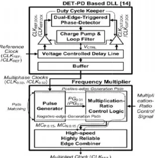
III EXISTING SYSTEM
International Journal of Science Engineering and Advance
Technology, IJSEAT, Vol. 6, Issue 6
ISSN 2321-6905
JUNE- 2018
a duplication - proportion control rationale, and an edge combiner. The double edge-activated stage locator thinks about both the positive and the negative edges of CLKREF, DCK and CLKOUT, DCK, which are the obligation cycle recovered tickers of CLKREF and CLKOUT using the obligation cycle administrator. The DLL is secured with 300 cycles in all procedure voltage-temperature corners inferable from the double edge recognition attributes, and creates 32-stage differential tickers (CLK0:32 and/CLK032). Using the 32-stage differential timekeepers, the beat generator create beats (PG0:31 and/PG0:31) for positive-edge and negative edge age. The augmentation proportion control rationale picks suitable heartbeats from PG0:31 and PG0:31 and produces MCP, 0:15 and MCN, 0:15 as per the duplication proportion control flag.
Fig. 3(a) structure of the clock generator.
At long lost, the high-speed and highly reliable edge combiner (HSHR-EC) produces one multiplied clock (CLKMUL) utilizing every one of the outputs of the multiplication ratio control logic. Since the number of multiphase is 32, the maximum multiplication ratio is 16. To comprehend the speed and the reliability issues of past edge combiners, an HSHREC, which includes a pre combining stage, overlap canceller, and push-pull stage, as shown in Fig. 3(b), is proposed. The two-step edge combiner, pre combining, and push-pull stage are utilized to upgrade the maximum multiplied clock frequency. The overlap canceller is utilized to ensure the stable operation of the frequency multiplier. Fig. 3(c) shows the operation of the HSHR-EC.
Fig. 3(b) structure of the proposed HSHR-EC.
Fig. 3(c) Operation of the proposed HSHR-EC. IV PROPOSED TECHNICH
XOR Phase detector
Fig. 4.1 simple circuit diagram of XOR gate
The output of an exclusive OR gate is only high (1) when the first OR the other input two is high (1). On the off chance that the two inputs have the same logical state, either high (1) or low (0) the output of an XOR gate is low (0). This can be simplified in saying that the output of an exclusive OR gate is low (0) if the input states are same. On the off chance that the input states are different, the output will be high (1).If one applies a rectangular signal with identical parameters, for example, frequency and amplitude, to an XOR gate, the output of the XOR gate will be a logical 0 if the phase difference between the two signals is 0 degrees .This
International Journal of Science Engineering and Advance
Technology, IJSEAT, Vol. 6, Issue 6
ISSN 2321-6905
JUNE- 2018
a duplication - proportion control rationale, and an edge combiner. The double edge-activated stage locator thinks about both the positive and the negative edges of CLKREF, DCK and CLKOUT, DCK, which are the obligation cycle recovered tickers of CLKREF and CLKOUT using the obligation cycle administrator. The DLL is secured with 300 cycles in all procedure voltage-temperature corners inferable from the double edge recognition attributes, and creates 32-stage differential tickers (CLK0:32 and/CLK032). Using the 32-stage differential timekeepers, the beat generator create beats (PG0:31 and/PG0:31) for positive-edge and negative edge age. The augmentation proportion control rationale picks suitable heartbeats from PG0:31 and PG0:31 and produces MCP, 0:15 and MCN, 0:15 as per the duplication proportion control flag.
Fig. 3(a) structure of the clock generator.
At long lost, the high-speed and highly reliable edge combiner (HSHR-EC) produces one multiplied clock (CLKMUL) utilizing every one of the outputs of the multiplication ratio control logic. Since the number of multiphase is 32, the maximum multiplication ratio is 16. To comprehend the speed and the reliability issues of past edge combiners, an HSHREC, which includes a pre combining stage, overlap canceller, and push-pull stage, as shown in Fig. 3(b), is proposed. The two-step edge combiner, pre combining, and push-pull stage are utilized to upgrade the maximum multiplied clock frequency. The overlap canceller is utilized to ensure the stable operation of the frequency multiplier. Fig. 3(c) shows the operation of the HSHR-EC.
Fig. 3(b) structure of the proposed HSHR-EC.
Fig. 3(c) Operation of the proposed HSHR-EC. IV PROPOSED TECHNICH
XOR Phase detector
Fig. 4.1 simple circuit diagram of XOR gate
International Journal of Science Engineering and Advance
Technology, IJSEAT, Vol. 6, Issue 6
ISSN 2321-6905
JUNE- 2018
www.ijseat.com
Page 301
is on the grounds that the two signals have precisely the same logical state at any given point in time. The inverse happens if the signals have a phase difference of 180 degrees. 180 degrees phase difference implies that the second signal as an ideal reflection of the first signal. With 180 degrees phase difference the second signal will be at a logic low (0) state if the first signal is high (1) and the other way around. Since the signals have precisely inverse logical states at any given point in time, the output of the XOR gate will constantly be high (1).
Voltage controlled oscillator:
A voltage-controlled oscillator (VCO) is an electronic oscillator whose oscillation frequency is controlled by a voltage input. Connected input voltage decides the instantaneous oscillation frequency. Consequently, thus a VCO can be utilized for frequency modulation (FM) or phase modulation (PM) by applying a modulating signal to the control input. A VCO is additionally an integral part of a phase-locked loop. It produces a digital clock. The frequency of the clock produced is controlled by one or more voltage inputs.
Charge pump:
Charge pumps utilize some type of switching device to control the association of a supply voltage over a load through a capacitor. They are usually utilized a low-power electronics (for example mobile phones) to raise and lower voltages for various parts of the circuitry – limiting the power consumption by controlling supply voltages precisely. Loop filters decipher between the phase detector's measurement signal and the VCO's control voltage(s). On the off chance that output lags the input, accelerate the VCO. If the input lags the output, slow the VCO down.
Loop Filter:
The loop filter is most imperative of design in DPLL. It is comprised of a capacitor and a resistor. The Loop filter function is to determine loop dynamics, also called stability. This is the manner by which the loop reacts to disturbances, such as changes in the reference frequency, changes of the feedback divider, or at startup. Common considerations are the range over which the loop can achieve lock. It removes the unwanted frequency of the clock recovery.
Proposed frequency multiplier:
The proposed frequency multiplier is composed of 59 MHZ DPPLL for high frequency multiplied clock generation. The proposed frequency multiplier is composed of a pulse generator and a XOR phase detector,and edge combiner and multiplication ratio control logic. In which the XOR is utilized to decrease the propagation delay.The phase-detector
compares both the positive and the negative edge of CLKREF, DCK and CLKOUT, DCK, which are duty cycle recovered clocks of CLKREF and CLKOUT utilizing the duty-cycle manager. The DPLL is locked with in 200 cycles in all process-voltage-temperature corners, and generates 59-phase differential clocks (CLK0:59 and/CLK0:59). Utilizing the 59-phase differential clocks, the pulse generator produces pulses for positive-edge and negative edge generation. The multiplication-ratio control logic chooses appropriate pulses from outputs of pulse generator and generates MCP, 0:30 and MCN,0:30 as indicated by the multiplication ratio control signal. The structure of the proposed frequency multiplier is shown in Fig. 4.2.
Fig.4.2 proposed frequency multiplier.
In which the high-speed and highly reliable edge combiner (HSHR-EC) is embraced from existing system and the design is same as the existing high speed and highly reliable edge combiner. It produces multiplied clock (CLKMUL) utilizing every one of the outputs of the multiplication ratio control logic. HSHR-EC relies upon voltage, frequency, and multiplication ratio control logic. Since the number of multiphase is 59, the maximum multiplication ratio is 33. To understand the speed and the reliability issues of past edge combiners, an HSHREC, which comprises of a pre combining stage, overlap canceller, and push-pull stage, as shown in Fig. 3(c), is adopted. The two-step edge combiner, pre combining, and push-pull stage are utilized to upgrade the maximum multiplied clock frequency. The overlap canceller is utilized to ensure the stable operation of the frequency multiplier. It composed of a NAND and NOR gates to remove the pulse overlapping.
International Journal of Science Engineering and Advance
Technology, IJSEAT, Vol. 6, Issue 6
ISSN 2321-6905
JUNE- 2018
www.ijseat.com
Page 301
is on the grounds that the two signals have precisely the same logical state at any given point in time. The inverse happens if the signals have a phase difference of 180 degrees. 180 degrees phase difference implies that the second signal as an ideal reflection of the first signal. With 180 degrees phase difference the second signal will be at a logic low (0) state if the first signal is high (1) and the other way around. Since the signals have precisely inverse logical states at any given point in time, the output of the XOR gate will constantly be high (1).
Voltage controlled oscillator:
A voltage-controlled oscillator (VCO) is an electronic oscillator whose oscillation frequency is controlled by a voltage input. Connected input voltage decides the instantaneous oscillation frequency. Consequently, thus a VCO can be utilized for frequency modulation (FM) or phase modulation (PM) by applying a modulating signal to the control input. A VCO is additionally an integral part of a phase-locked loop. It produces a digital clock. The frequency of the clock produced is controlled by one or more voltage inputs.
Charge pump:
Charge pumps utilize some type of switching device to control the association of a supply voltage over a load through a capacitor. They are usually utilized a low-power electronics (for example mobile phones) to raise and lower voltages for various parts of the circuitry – limiting the power consumption by controlling supply voltages precisely. Loop filters decipher between the phase detector's measurement signal and the VCO's control voltage(s). On the off chance that output lags the input, accelerate the VCO. If the input lags the output, slow the VCO down.
Loop Filter:
The loop filter is most imperative of design in DPLL. It is comprised of a capacitor and a resistor. The Loop filter function is to determine loop dynamics, also called stability. This is the manner by which the loop reacts to disturbances, such as changes in the reference frequency, changes of the feedback divider, or at startup. Common considerations are the range over which the loop can achieve lock. It removes the unwanted frequency of the clock recovery.
Proposed frequency multiplier:
The proposed frequency multiplier is composed of 59 MHZ DPPLL for high frequency multiplied clock generation. The proposed frequency multiplier is composed of a pulse generator and a XOR phase detector,and edge combiner and multiplication ratio control logic. In which the XOR is utilized to decrease the propagation delay.The phase-detector
compares both the positive and the negative edge of CLKREF, DCK and CLKOUT, DCK, which are duty cycle recovered clocks of CLKREF and CLKOUT utilizing the duty-cycle manager. The DPLL is locked with in 200 cycles in all process-voltage-temperature corners, and generates 59-phase differential clocks (CLK0:59 and/CLK0:59). Utilizing the 59-phase differential clocks, the pulse generator produces pulses for positive-edge and negative edge generation. The multiplication-ratio control logic chooses appropriate pulses from outputs of pulse generator and generates MCP, 0:30 and MCN,0:30 as indicated by the multiplication ratio control signal. The structure of the proposed frequency multiplier is shown in Fig. 4.2.
Fig.4.2 proposed frequency multiplier.
International Journal of Science Engineering and Advance
Technology, IJSEAT, Vol. 6, Issue 6
ISSN 2321-6905
JUNE- 2018
V. Design and simulation results
The proposed frequency multiplier was designed and simulated using MICROWIND dsch2. The results are shown in Fig. 5(a) XOR phase detector, 5(b) design of voltage controlled oscillator, 5(c) design of adc,5(d) loop filter, 5(e) design of DPLL ,5(f) Output wave form of DPLL, 5(g) Layout of DPLL ,5(h) layout waveform, 5(i) voltage vs currents, 5(j) Frequency vs Time.
5(a)
5(b)
5(c)
5(d)
5(e)
5(f)
5(g)
International Journal of Science Engineering and Advance
Technology, IJSEAT, Vol. 6, Issue 6
ISSN 2321-6905
JUNE- 2018
www.ijseat.com
Page 303
5(i)
5(j)
VI. MEASUREMENT RESULTS
The proposed frequency multiplier is executed utilizing a 0.12μm CMOS process technology, and has a supply voltage is1.2v. The proposed frequency multiplier has the maximum multiplication ratio is 33 and maximum multiplied clock frequency is 60 MHz and it generates 59 differential multiphase clocks.
VI COMPARISION.
VII CONCLUSION
In this paper, low power and high speed and highly reliable frequency multiplier based on DPLL is proposed. The proposed engineering produces the rapid activity because of its progressive edge-combiner structure and exceedingly solid task because of cover canceller and the proposed recurrence multiplier limits the defer distinction between positive – and negative-edge age ways. At
long last, a numerical investigation is performed to approve its execution. The recurrence multiplier,
which is created using the 0.12μm CMOS process
innovation, has the most extreme increase proportion is 33 and a yield go is 100MHz, and a power utilization to a recurrence proportion of 0.698mw.
REFERENCES:
[1] Yu-Qing Bao and Yang Li, “FPGA-Based Design
of Grid Friendly Appliance Controller,”IEEE
TRANSACTIONS ON SMART GRID VOL .5, NO.2, MARCH 2014.
[2] Chao-Wen Tzeng, Shi-Yu Huang, “Parameterized
All-Digital PLL Architecture and its Compiler to
Support Easy Process Migration”IEEE
TRANSACTIONS ON VERY LARGE SCALE INTEGRATION (VLSI) SYSTEMS, VOL.22, NO.3, MARCH 2014
[3] Wei Deng Ahmed Musa, TeerachotSiriburanon , Masaya Miyahara , Kenichi Okada and Akira
Matsuzawa, “A Dual-loop Injectionlocked PLL with ALL-digital Background Calibration System for On-chip Clock Generation”,2014 IEEE.
[4] Ba You Jie Wang Songyang Li, “ FPGA-Based Induction heating with Variable Modulus Control All-Digital Phase-Locked Loop Research”2013 2nd
International Conference on Measurement, Information and Control.
[5] C.-C. Chung and C.-Y. Lee, “An all-digital
phase-locked loop for high speed Clock generation,” IEEE
J. Solid-State Circuits, vol. 38, no. 2, pp. 347–351, Feb. 2003.
[6] T. Olsson and P. Nilsson, “A digitally controlled PLL for SoC applications,” IEEE J. Solid-State Circuits, vol. 39, no. 5, pp. 751–760, May 2004.
[7] M. Combs, K. Dioury, and A. Greiner, “A
portable clock multiplier Generator using digital
CMOS standard cells,” IEEE
[8] K. Ryu, D. H. Jung, and S.-O. Jung, “A DLL
based clock generator for low-power mobile SoCs,”
IEEE Trans. Consum. Electron., vol. 56, no. 3, pp. 1950–1956, Aug. 2010.
[9] K. Ryu, D. H. Jung, and S.-O. Jung, “A DLL with
dual edge triggered phase detector for fast lock and
low jitter clock generator, ” IEEE Trans. Circuits
International Journal of Science Engineering and Advance
Technology, IJSEAT, Vol. 6, Issue 6
ISSN 2321-6905
JUNE- 2018
[10] D. Birru, “A novel delay-locked loop based
CMOS clock multiplier,” IEEE Trans. Consumer
Electron., vol. 44, no. 4, pp. 1319-1322, Nov. 1998.
[11] G. Chien and P. R. Gray, “A 900-MHz local oscillator using a DLL- based frequency multiplier
technique for PCS applications,” IEEE J. Solid-State Circuits , vol. 35,no. 12, pp. 1996–1999, Dec. 2000
[12] D. J. Foley and M. P. Flynn, “C MOS DLL -based 2-V 3.2-ps jitter 1- GHz clock synthesizer and temperaturecompensatedtunable oscillator,” IEEE J.
Solid-State Circuits, vol. 36, no. 3, pp. 417–423, Mar. 2001.
[13] S. Ok, K. Chung, J. Koo and C. Kim, “An
antiharmonic, programmable, DLL-based frequency
multiplier for dynamic frequency scaling,” IEEE
Trans. Very Large Scale Integr. (VLSI) Syst. , vol. 18, no. 7, pp. 1130–1134, Jul. 2010.
[14] J. Koo, S. Ok, and C. Kim, “A low-power programmable DLL-based clock generator with wide-range antiharmonic lock,” IEEE Tran.Circuits
Syst. II, Exp. Briefs, vol. 56, no. 1, pp. 21–25, Jan. 2009.
[15] A. Elshazly, R. Inti, B. Young, and P. K.
Hanumolu, “Clock multiplication techniques using
digital multiplying delay-locked loops,” IEEE J.