1Department of Mechanical and Materials Engineering, University of Nebraska-Lincoln, Lincoln, NE, USA. 2Department of Physics and Astronomy, and Nebraska Center for Materials and Nanoscience, University of Nebraska-Lincoln, Lincoln, NE, USA. 3Computational Laboratory for Hybrid/Organic Photovoltaics (CLHYO), CNR-ISTM, Perugia, Italy. 4D3-Computation, Istituto Italiano di Tecnologia, Genova, Italy. 5Department of Applied Physical Sciences, University of North Carolina, Chapel Hill, NC, USA. 6These authors contributed equally: Bo Chen, Tao Li. *e-mail: [email protected]; [email protected]
O
rganic–inorganic hybrid perovskites (OIHPs) have attracted extensive interest for potential use in next-generation photo-voltaic devices due to the demonstrated high power conver-sion efficiency, low materials cost and low fabrication cost1,2. OIHP materials display extraordinary optoelectronic properties, such as a large absorption coefficient, high carrier mobility and long carrier recombination lifetimes, which benefit their outstanding perfor-mance in solar cells, photodetectors, X-ray detectors, γ -ray detec-tors and light-emitting diodes (LEDs)3–9. Solar cells based on OIHP thin films have achieved a certified power conversion efficiency of 23.3%2. OIHP photodetectors based on MAPbI3 thin films demon-strate high specific detectivity, a low detection limit of 0.64 pW cm−2 and ultrafast sub-nanosecond response time3,4. The strong surface-charge recombination enables a unique narrow spectral response with full-width at half-maximum of less than 20 nm in OIHP single-crystal photodetectors5. Due to the high mobility–lifetime product (µτ) and large atomic number, MAPbBr3 single-crystal X-ray detec-tors have shown a high sensitivity of 2.1 × 10⁴µ C Gy
air−1 cm−2 under 8 keV X-ray radiation, which is over a thousand times better than commercial amorphous selenium X-ray detectors6. The dopant-compensated MAPbBr2.94Cl0.06 single crystals have dramatically reduced the free carrier concentration and increased the carrier mobility, yielding an outstanding γ -ray spectrometer with a resolu-tion comparable to that of a standard scintillator γ -ray detector7. OIHP LEDs have demonstrated tunable emission wavelengths, a maximum external quantum efficiency of 10.4% and the largest peak luminance of 20,000 cd m–28,9.
For conventional inorganic perovskites, commercial appli-cations mainly rely on the strong electromechanical coupling, including both piezoelectricity and electrostriction. The direct
piezoelectric effect converts mechanical energy into electrical energy, with applications in piezoelectric sensors and piezoelectric generators10. For example, a sonar system based on piezoelectric sensors could transmit and receive ultrasonic signals for under-water communication. Piezoelectric generators have been used for ignition in lighters and also to harvest mechanical energy at both macroscopic scales and nanoscales11. The inverse piezoelec-tric effect creates material deformation under an applied elecpiezoelec-tric field, which enables many applications of piezoelectric actuators, such as accurate position controllers for optical cameras and tele-scopes, and ultrasound generation for ultrasonic cleaning systems and sonars12. Electrostriction is an electromechanical coupling with strain proportional to the square of applied electric field, while piezoelectric strain is linear with applied electric field. Two types of electrostrictive material have been explored, including relaxor ferroelectric ceramics and electrostrictive polymers13–27. Electrostriction can allow a material to achieve larger strain at high applied fields than does piezoelectricity. The piezoelectric strain is typically of the order of 0.1%, while electrostrictive materials can achieve a strain of 5% or more13–27.
OIHPs possess a similar lattice structure to conventional inor-ganic perovskites; however, the electromechanical coupling of OIHPs has barely been explored. Here, we report the observation of a strong electromechanical response of MAPbI3 single crys-tals. The measured electromechanical strain is proportional to the square of electric field, which indicates an electrostrictive property of MAPbI3. It has been found that the MAPbI3 single crystal exhibits a compressive strain of up to 1% with a mechanical energy density of 0.74 J cm−3, which is higher than that of most existing electrostric-tive materials.
Large electrostrictive response in lead
halide perovskites
Bo Chen
1,6, Tao Li
2,6, Qingfeng Dong
1, Edoardo Mosconi
3,4, Jingfeng Song
2, Zhaolai Chen
1,
Yehao Deng
1, Ye Liu
1, Stephen Ducharme
2, Alexei Gruverman
2, Filippo De Angelis
3,4* and
Jinsong Huang
1,5*
Lead halide perovskites have demonstrated outstanding performance in photovoltaics, photodetectors, radiation detectors and light-emitting diodes. However, the electromechanical properties, which are the main application of inorganic perovskites, have rarely been explored for lead halide perovskites. Here, we report the discovery of a large electrostrictive response in
methylam-monium lead triiodide (MAPbI3) single crystals. Under an electric field of 3.7 V µ m−1, MAPbI3 shows a large compressive strain
of 1%, corresponding to a mechanical energy density of 0.74 J cm−3, comparable to that of human muscles. The influences of
piezoelectricity, thermal expansion, intrinsic electrostrictive effect, Maxwell stress, ferroelectricity, local polar fluctuation and methylammonium cation ordering on this electromechanical response are excluded. We speculate, using density functional
theory, that electrostriction of MAPbI3 probably originates from lattice deformation due to formation of additional defects
High electrostriction in MAPbi
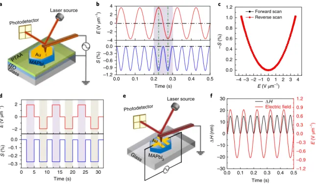
3We detected a high strain induced by electric field in MAPbI3 single crystals under a field of less than 10 V µ m−1 by atomic force micros-copy (AFM) measurement (Fig. 1). MAPbI3 single crystals with thickness of 40 µ m were grown directly on a poly(bis(4-phenyl) (2,4,6-trimethylphenyl)amine)- (PTAA-) coated indium tin oxide (ITO)–glass substrate using a non-wetting surface-induced space-confined method28. Under an a.c. electric field of 3.7 V µ m−1 with a frequency of 10 Hz, the MAPbI3 single crystal shows thickness oscil-lation with the maximum amplitude corresponding to 1% strain (Fig. 1b). It is noted that MAPbI3 single crystals contract under both positive and negative bias irrespective of the field polarity, which is also confirmed with a d.c. bias pulse in Fig. 1d. As a result, the fre-quency of the strain induced by electric field is twice the applied a.c. bias. The magnitude of field-induced strain could be easily tuned by changing the amplitude of the a.c. bias (Supplementary Fig. 1). We measured the magnitude of strain under different fields. As shown in Fig. 1c, the strain (S) and electric field (E) showed a quadratic relationship:
= ×
S M E2 (1)
where M is the electrostrictive coefficient. This quadratic rela-tionship indicates that the electromechanical response here is dominated by electrostriction. The calculated electrostrictive coefficient is − 730 nm2 V−2 for MAPbI
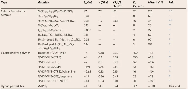
3 single crystals, which is the largest among all reported electrostrictive materials, with details summarized in Table 1. For the most popular electrostric-tive ceramic, Pb(Zn1/3Nb2/3)O3–8% PbTiO3, and electrostrictive polymer, P(VDF–TrFE)/CuPc, the electrostrictive coefficient is 120 nm2 V−2 and − 113 nm2 V−2, respectively16,24. The large elec-trostrictive response allows observation of material shape change with the naked eye (Supplementary Video 1). Supplementary Video 1 also shows that some strip lines appeared on the sur-faces of a MAPbI3 crystal under applied pulse bias29, which can be
explained by twin formation under the high electrostrictive strain induced by the applied field. Twin structures have been previously observed in both single-crystalline and polycrystalline MAPbI3 due to the ferroelastic properties of this material30.
Superior to other electrostrictive materials, MAPbI3 demon-strates both high electrostrictive strain and large elastic energy den-sities under a small applied field (as shown in Table 1). However, for other electrostrictive materials, tens or even thousands of volts per micrometre are required to achieve comparable electrostrictive strain or elastic energy density. The electrostrictive strain for relaxor ferroelectric ceramics is of the order of 0.1%13–20. Electrostrictive polymers display electrostrictive strain exceeding 5% with elas-tic energy density of the order of 0.1 J cm−3; however, the elec-trostrictive polymers require high operation field of more than 100 V µ m−1 21–23. Raising the polarization density by introducing materials with high dielectric constant into a P(VDF–TrFE) matrix to form electrostrictive polymer composites can reduce the electric field needed to approach 5% strain to tens of volts per micrometre, while their low Young’s modulus (< 1 GPa) limits the elastic energy densities less than 0.5 J cm−324–27. Although the electrostrictive strain of MAPbI3 is only 1%, its large electrostrictive coefficient and rela-tively large Young’s modulus of 14.8 GPa (Supplementary Fig. 2) enable MAPbI3 single crystals to achieve a record high mechanical energy density of 0.74 J cm−3 under an applied electric field of only 3.7 V µ m−1. This mechanical energy density is comparable to that of human muscles, and on a par with typical actuator materials (0.016 to 1.0 J cm−3)31–34.
The contraction of perovskite crystals along the direction of the applied field may be accompanied by expansion of the crystal lattice in the direction perpendicular to the applied electric field, which is determined by the components of the piezoelectric and electrostric-tion tensors. In order to measure it, we fabricated lateral-structure devices with two Au electrodes on the top surface of MAPbI3 sin-gle crystals, as illustrated in Fig. 1e. The in-plane electric field was applied in parallel with the crystal surface, while the crystal thickness
0.0 0.1 0.2 0.3 0.4 0.5
–1.2 –0.9 –0.6 –0.3 0.0 –4 –2 0 2 4 S (%) –S (%) Time (s) E (V µ m –1)
–4 –3 –2 –1 0 1 2 3 4 0.0 0.2 0.4 0.6 0.8 1.0 1.2
E (V µm–1)
E (V µ m –1) E (V µ m –1) Forward scan Reverse scan b a Laser source
Laser source f
e d
c
0.0 0.1 0.2 0.3 0.4 0.5
–30 –20 –10 0 10 20 30 Time (s) ∆ H (nm) ∆H Electric field –1.2 –0.9 –0.6 –0.3 0.0 0.3 0.6 0.9 1.2 –2 0 2
0 5 10 15 20 25 30
–0.3 –0.2 –0.1 0.0 S (%) Time (s) Photodetector Photodetector PTAA
ITO MAPbI3
MAPbI 3 Au Au Glass Glass
Fig. 1 |Electrostrictive response of MAPbi3 single crystal.a, Schematic illustration of AFM measurement of strain induced by electric field.
change along the out-of-plane direction was monitored by the AFM tip. We found that the MAPbI3 single crystal expands along the out-of-plane direction (Fig. 1f).
Macroscopic measurement of electrostrictive response
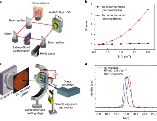
The macroscopic strain of the crystals was measured directly with laser interferometry to verify the strain in the perovskite crystals under bias. The geometry of measurement is shown in Fig. 2a. It is worth pointing out that both piezoelectric effect and electrostric-tion can cause an electromechanical response, while they can be distinguished by their different field-dependent strain relationships (Supplementary Section 1.0). Piezoelectricity is a first-order tromechanical coupling where the strain is proportional to the elec-tric field, while electroselec-triction is second-order coupling in which the strain is proportional to the square of the electric field. Here we measured the strain dependent on electric field at 100 Hz. The fre-quency of 100 Hz was chosen to obtain a large signal-to-noise ratio and thus a reliable reading in the piezoelectric response. As shown in Fig. 2b, the MAPbI3 singe crystal shows both piezoelectric and electrostrictive responses. The electrostrictive response is one order of magnitude stronger than the piezoelectric response (Fig. 2b). The first-order piezoelectric response is small, with a piezoelectric coefficient (d33) of 3.1 pm V−1. This d33 value is very close to a previ-ously measured value of 2.7 pm V−1 at a higher frequency of 1 kHz29, and in excellent agreement with the value calculated in ref. 35. The occurrence of a high electrostrictive strain should be detected by X-ray diffraction (XRD). Figure 2c shows the geometry of XRD characterization of a MAPbI3 single crystal under an electric field of 2.5 V µ m−1. As shown in Fig. 2d, a shift of the XRD peak for the (200) plane to a larger diffraction angle is indeed observed when the MAPbI3 single crystal is under an applied field along the out-of-plane direction, which confirms the contraction of the lattice along the field direction. The XRD peak shift direction is opposite to that caused by the thermal expansion, because thermal expansion of the MAPbI3 single crystal should shift the XRD peaks to smaller dif-fraction angles (Fig. 2d). This excludes thermal expansion as the
origin of the electromechanical response of the MAPbI3 single crys-tals under applied bias.
Stability and temporal response of electrostriction
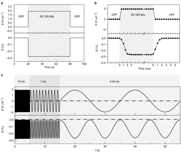
In order to evaluate the strain stability and response time of elec-trostriction for the MAPbI3 single crystals, we applied a rectan-gular-shaped bias pulse with a duration of 60 s and measured the resulting strain with the AFM tip. When the d.c. bias was switched on, the electrostrictive strain appeared immediately and remained unchanged after 60 s (Fig. 3a). The electrostrictive performance was also found to be highly repeatable during 1200 actuation loops under an a.c. applied bias (Supplementary Fig. 3). Therefore, the MAPbI3 single crystals have stable electrostrictive response under applied field. The quick response of AFM (< 0.5 ms, E–t curve in Fig. 3b) allows us to examine the dynamics of the field-induced electrostrictive deformation. We found that the electrostrictive response time of the MAPbI3 single crystals is several milliseconds (Fig. 3b). As a result, the electrostrictive strain was fast enough to follow the change of electric field under a.c. bias with a frequency of up to 10 Hz (Fig. 3c). However, when the frequency of a.c. bias is increased to the kilohertz range, the electrostrictive strain cannot follow the change of electric field, and the electrostrictive response is negligible. This was verified using laser interferometer measure-ment, with results shown in Supplementary Fig. 4.
Mechanism of electrostriction in MAPbi
3single crystal
Here we consider two possible reported mechanisms, the intrinsic electrostrictive effect and Maxwell stress effect13–27, for the basic observation that the measured strain is proportional to the square of the applied voltage for MAPbI3 (Equation 1). However, we find that the electrostriction of the MAPbI3 single crystal cannot be explained by either of them. The intrinsic electrostrictive effect, due to anharmonic displacement of positive ions and negative ions under applied bias, dominates the electrostrictive response of relaxor ferroelectrics, and it induces lattice expansion instead of compres-sion, because the energy required to compress the ionic bonds is
Table 1 | Comparison of electrostrictive response of relaxor ferroelectric ceramic, electrostrictive polymers and MAPbi3 hybrid perovskite
Type Materials Sm (%) Y (GPa) YSm2/2
(J cm−3)
Em (V µ m−1)
M (nm2 V−2) ref.
Relaxor ferroelectric
ceramic Pb(Zn1/3Nb2/3)O3–8% PbTiO3 1.7 7.7 1.11 12 120
16,21
Pb(Zn1/3Nb2/3)O3 0.44 — — 8 69 17
Pb(Mg1/3Nb2/3)O3–0.27 PbTiO3 0.34 115 0.66 10 34 18,19
Pb(Mg1/3Nb2/3)O3 0.13 — — 8 20 20
K0.5Na0.5NbO3–SrTiO3 0.006 — — 2 15 13
Bi0.5Na0.5TiO3–BaTiO3–KNbO3 0.11 — — 4 69 14
5% Sn-doped Bi1/2(Na0.82K0.18)1/2TiO3 0.32 — — 6 90 13
2% Fe-doped Ba(Zr0.2Ti0.8)O3– 0.5(Ba0.7Ca0.3)TiO3
0.14 — — 3 156 15
Electrostrictive polymer Irradiated P(VDF–TrFE) − 4 0.38 0.30 150 − 1.8 21
P(VDF–TrFE–CTFE) − 4 0.4 0.32 150 − 1.8 22
P(VDF–TrFE–CFE) − 7 0.3 0.73 165 − 2.6 23
P(VDF–TrFE)/CuPc − 1.91 0.75 0.14 13 − 113 24
P(VDF–TrFE–CTFE)/polyaniline − 2.65 0.53 0.19 16 − 104 25
P(VDF–TrFE–CFE)/graphene − 4.1 0.56 0.47 23 − 78 26
P(VDF–TrFE–CFE)/DEHP − 1.8 0.04 0.01 10 − 180 27
Hybrid perovskites MAPbI3 − 1 14.8 0.74 3.7 − 730 This work
generally larger than that to expand the ionic bonds20,36. This cre-ates positive strain for relaxor ferroelectrics under bias (as summa-rized in Table 1), which contradicts the negative strain for MAPbI3 observed in our study. Moreover, the response time of ion displace-ment due to bond elongation inside the unit cell is reported to be in the microsecond range37, which is orders of magnitude faster than what is measured here. Therefore, the intrinsic electrostrictive effect cannot be the sole origin of the large electrostriction in MAPbI3.
Maxwell stress is caused by Coulombic interaction between uncompensated charges (due to imperfect screening) on the elec-trodes24. The strain induced by Maxwell stress (S
Maxwell) can be cal-culated from
εε ν
=− ∕ × + ∕
SMaxwell 1 2 0(1 2 )E Y2 (2) where ε is the relative dielectric permittivity, ε0 is the vacuum dielectric permittivity and ν is the Poisson ratio24. Using the Young’s modulus of 14.8 GPa and the Poisson ratio of 0.3338, an ε value of 1,500,000 is required for MAPbI3 to generate a strain of 1% under 3.7 V µ m−1, which is at least four orders of magnitude higher than the reported dielectric permittivity value for MAPbI3 (ε= 30–70)39,40. Migration of ions under applied electric field may cause ion accu-mulation at perovskite–electrode interfaces, which could also induce Maxwell strain. However, we found that accumulated ions at the interface cannot generate such high strain (Supplementary Information Section 6.0). Moreover, the amount of ion accumu-lation would increase with the bias duration, and a reverse bias is needed to remove the accumulated ions. The stable electrostric-tive strain output under bias and hysteresis-free strain–field rela-tion further qualitatively rule out ion accumularela-tion at the interface as the dominating mechanism for the electrostriction. This reveals
that the Maxwell stress effect is probably not significant for the elec-tromechanical response of the MAPbI3 device.
We further considered the impact of methylammonium cation (MA+) ordering, local polar fluctuations and ferroelectric polar-ization switching under an applied electric field on the electrome-chanical response. Considering that the calculated energy barrier for structural inversion induced by MA+ ordering is of the order of 20 meV (Supplementary Information Section 7.0), the MA cation reorientation occurs on the picosecond timescale41,42, which does not account for the much slower response observed here. Moreover, when replacing the polar MA+ with non-polar Cs+, we found that CsPbI3 also demonstrated electrostriction characteristics under applied bias (Supplementary Fig. 7). This excludes a major contri-bution of MA+ ordering to the electrostriction of OIHPs. In addi-tion to organic dipoles, local polar fluctuaaddi-tions, such as rotaaddi-tional disordering of I atoms in the PbI64− octahedra43 and head-to-head Cs motion coupled to lattice expansion44, is also several orders of magnitude faster than the observed electromechanical response of MAPbI3 reported here. We further investigated the electrostrictive response of cubic MAPbBr3, which has centrosymmetric struc-ture and thus is not ferroelectric, and this also demonstrated high electrostrictive strain under applied bias (Supplementary Fig. 8), which excludes a dominant impact of the ferroelectric effect on the electrostriction of OIHPs. The hysteresis-free strain–field relation further verifies that the electrostriction of OIHPs is not related to ferroelectricity.
Considering that the observed millisecond timescale for the electrostrictive response is close to that typically associated with ion/defect migration in OIHPs, we speculate that the observed elec-trostriction is related to defect formation. Long-range ion migra-tion under electric field cannot change the shape of the material,
b a
d
18.9 19.2 19.5 19.8 20.1 20.4 20.7
Intens
ity
(a
.u.)
2θ (°) RT w/o bias RT with 2.5 V µm–1
100°C w/o bias
0.0 0.5 1.0 1.5 2.0
0 2 4 6 8
Beam splitter
Beam splitter
HeNe Laser
Goniometer and heating stage
Sample alignment and monitor
X-ray generator X-ray
Mirror
2D detector
2D diffractionpattern
Babinet-Soleil Compensator
Photodetector
Au/MAPbl3/PTAA
∆
H
(n
m)
E (V µm–1)
1st order harmonic (piezoelectricity) 2nd order harmonic (electrostriction)
c
Fig. 2 |Macroscopic measurement of electrostrictive response for MAPbi3 single crystal.a, Schematic illustration of Mach–Zehnder interferometer
because ions would only move to a different crystal region with-out changing the crystal volume or strain. It has been reported that MAPbI3 has small ionic point defect formation energies45,46. We propose that lattice deformation is possibly caused by forma-tion of addiforma-tional defects, probably iodine Frenkel pairs, under electric field, and that this generates an electromechanical response in OIHPs. Computation (Supplementary Figs. 9–14) shows that the formation of iodine Frenkel defects under electric field could induce a strain of + 0.3% along the a/b axis and of − 0.6% along the c axis (Supplementary Fig. 11), comparable to the experimen-tally measured electrostrictive strain. Upon removing the electric field the starting pristine situation is restored (Supplementary Fig. 11d), due to the attraction and annihilation between the oppo-sitely charged defects. The Arrhenius relation between the elec-trostrictive response and temperature (Supplementary Fig. 15) and reduction of effective activation energy for ion migration in perovskite with increasing field (Supplementary Fig. 16) provide a connection between electrostriction and defect formation/annihila-tion, lending support to the proposed mechanism.
Outlook
Since almost every electronic device either operates under applied electric field or experiences an internal built-in field, which is close to the field of 3.7 V µ m−1 inducing 1% strain, the discovery of electrostriction and its origin may also impact the design and performance of OIHP-based electronic devices, including solar
cells, LEDs, photodetectors and radiation detectors. For perovskite solar cells, we recently found that the presence of remnant lattice strain in OIHP polycrystalline films could accelerate their degra-dation under illumination47. The electrostrictive strain of OIHP polycrystalline films is expected to impact the stability of perovskite solar cells by adding additional strain to perovskite grains. For a typical perovskite solar cell with open-circuit voltage of 1.08–1.15 V and OIHP film thickness of 300–500 nm, the built-in electric field under the maximum power point condition is 0.30–0.65 V µ m−1. This could generate an electrostrictive strain of about 0.01–0.03% at the maximum power point condition based on an electrostric-tive coefficient of –730 nm2 V−2. We have recently reported that polycrystalline MAPbI3 films have tensile strain (~0.47%) in the in-plane direction, which is formed in the cooling process due to mismatched thermal expansion of MAPbI3 with the substrate47. In this case, the electrostriction sets a new stable state with a larger lattice along the in-plane direction, which thus reduces the tensile strain caused by thermal annealing and improves the device stabil-ity. We also find that some perovskite films (such as FA0.85MA0.15Pb (I0.85Br0.15)3) have much less or no annealing-induced remnant lat-tice strain. Therefore, electrostrictive strain could accelerate device degradation, though the impact will not be significant due to the small electrostrictive strain induced. Similarly, the electrostrictive strain changes the ion migration rate in OIHPs, and thus will also impact the stability of LEDs and detectors. The field-induced defect generation also sets a lower limit of carrier concentration in hybrid
DC ON 60s OFF
OFF
0.05 Hz 1 Hz
10 Hz
b
c
DC ON 60s OFF
OFF a
–2 0 2
–0.4 –0.3 –0.2 –0.1 0.0
E
(V
µ
m
–1)
S
(%)
Time (ms) 0
0 1 2 3 1 2 3 4 5
–2 –1 0 1 2
0 10 20 30 40 50
–0.3 –0.2 –0.1 0.0
E
(V
µ
m
–1)
S
(%)
t (s) –0.5
0.0 0.5 1.0 1.5 2.0 2.5
0 20 40 60 80 100
–0.3 –0.2 –0.1 0.0
E
(V
µ
m
–1)
S
(%)
Time (s)
perovskites. Since a high dark conductivity is crucial for detectors such as radiation detectors, strategies to mitigate the electrostric-tion effect would be needed to design single-photon detectors using OHIPs. The electron–phonon interaction has been reported to be crucial in determining several unique properties of OIHPs48, such as long hot-carrier relaxation lifetime in OIHP materials49. The electrostrictive strain is thus expected to have an influence on the carrier mobility and hot-carrier relaxation lifetime, which should be further studied in the future. Finally, the large electrostriction of MAPbI3 crystals could have a broad range of potential applications in, for example, actuators, sonar transducers and integrated micro-electromechanical systems.
Online content
Any methods, additional references, Nature Research reporting summaries, source data, statements of data availability and asso-ciated accession codes are available at https://doi.org/10.1038/
s41563-018-0170-x.
Received: 10 August 2017; Accepted: 16 August 2018; Published online: 24 September 2018
references
1. Yang, W. S. et al. Iodide management in formamidinium-lead-halide-based perovskite layers for efficient solar cells. Science 356, 1376–1379 (2017). 2. NREL Best research-cell efficiencies. https://www.nrel.gov/pv/assets/images/
efficiency-chart-20180716.jpg (accessed 16 July 2018).
3. Fang, Y. & Huang, J. Resolving weak light of sub-picowatt per square centimeter by hybrid perovskite photodetectors enabled by noise reduction.
Adv. Mater. 27, 2804–2810 (2015).
4. Shen, L. et al. A self-powered, sub-nanosecond-response solution-processed hybrid perovskite photodetector for time-resolved photoluminescence-lifetime detection. Adv. Mater. 28, 10794–10800 (2016).
5. Fang, Y., Dong, Q., Shao, Y., Yuan, Y. & Huang, J. Highly narrowband perovskite single-crystal photodetectors enabled by surface-charge recombination. Nat. Photon. 9, 679–686 (2015).
6. Wei, W. et al. Monolithic integration of hybrid perovskite single crystals with heterogeneous substrate for highly sensitive X-ray imaging. Nat. Photon. 11, 315–321 (2017).
7. Wei, H. et al. Dopant compensation in alloyed CH3NH3PbBr3-xClx perovskite single crystals for gamma-ray spectroscopy. Nat. Mater. 16, 826–833 (2017). 8. Sutherland, B. R. & Sargent, E. H. Perovskite photonic sources. Nat. Photon.
10, 295–302 (2016).
9. Xiao, Z. G. et al. Efficient perovskite light-emitting diodes featuring nanometre-sized crystallites. Nat. Photon. 11, 108–115 (2017). 10. Gautschi, G. Piezoelectric Sensorics (Springer, New York, 2002).
11. Wang, X., Song, J., Liu, J. & Wang, Z. L. Direct-current nanogenerator driven by ultrasonic waves. Science 316, 102–105 (2007).
12. Uchino, K. Piezoelectric Actuators and Ultrasonic Motors (Springer, New York, 1997).
13. Bobnar, V. et al. Electrostrictive effect in lead-free relaxor K0.5Na0.5NbO3– SrTiO3 ceramic system. J. Appl. Phys. 98, 024113–024113 (2005). 14. Wang, F. F., Jin, C. C., Yao, Q. R. & Shi, W. Z. Large electrostrictive
effect in ternary Bi0.5Na0.5TiO3-based solid solutions. J. Appl. Phys. 114, 027004 (2013).
15. Li, F., Jin, L. & Guo, R. High electrostrictive coefficient Q33 in lead-free Ba(Zr0. 2Ti0. 8)O3-x(Ba0. 7Ca0. 3)TiO3 piezoelectric ceramics. Appl. Phys. Lett. 105, 232903 (2014).
16. Park, S. E. & Shrout, T. R. Ultrahigh strain and piezoelectric behavior in relaxor based ferroelectric single crystals. J. Appl. Phys. 82, 1804–1811 (1997).
17. Li, F., Jin, L., Xu, Z., Wang, D. & Zhang, S. Electrostrictive effect in Pb(Mg1/3Nb2/3)O3-xPbTiO3 crystals. Appl. Phys. Lett. 102, 152910 (2013). 18. Li, F., Xu, Z. & Zhang, S. The effect of polar nanoregions on
electromechanical properties of relaxor-PbTiO3 crystals: extracting from electric-field-induced polarization and strain behaviors. Appl. Phys. Lett. 105, 122904 (2014).
19. Baek, S. et al. Giant piezoelectricity on Si for hyperactive MEMS. Science 334, 958–961 (2011).
20. Li, F., Jin, L., Xu, Z. & Zhang, S. Electrostrictive effect in ferroelectrics: an alternative approach to improve piezoelectricity. Appl. Phys. Rev. 1, 011103 (2014).
21. Zhang, Q. M., Bharti, V. & Zhao, X. Giant electrostriction and relaxor ferroelectric behavior in electron-irradiated poly(vinylidene fluoride-trifluoroethylene) copolymer. Science 280, 2101–2104 (1998).
22. Xu, H. S. et al. Ferroelectric and electromechanical properties of poly(vinylidene-fluoride-trifluoroethylene-chlorotrifluoroethylene) terpolymer. Appl. Phys. Lett. 78, 2360–2362 (2001).
23. Bauer, F., Fousson, E. & Zhang, Q. M. Recent advances in highly
electrostrictive P(VDF–TrFE–CFE) terpolymers. IEEE Trans. Dielectr. Electr. Insul. 13, 1149–1154 (2006).
24. Zhang, Q. M. et al. An all-organic composite actuator material with a high dielectric constant. Nature 419, 284–287 (2002).
25. Huang, C. & Zhang, Q. Enhanced dielectric and electromechanical responses in high dielectric constant all-polymer percolative composites. Adv. Funct. Mater. 14, 501–506 (2004).
26. Javadi, A., Xiao, Y., Xu, W. & Gong, S. Chemically modified graphene/ P(VDF–TrFE–CFE) electroactive polymer nanocomposites with superior electromechanical performance. J. Mater. Chem. 22, 830–834 (2012).
27. Le, M. Q. et al. All-organic electrostrictive polymer composites with low driving electrical voltages for micro-fluidic pump applications. Sci. Rep. 5, 11814 (2015).
28. Chen, Z. et al. Single crystal perovskite solar cells with broadened light-harvesting spectrum. Nat. Commun. 8, 1890 (2017).
29. Dong, Q. et al. Lateral-structure single-crystal hybrid perovskite solar cells via piezoelectric poling. Adv. Mater. 28, 2816–2821 (2016).
30. Strelcov, E. et al. CH3NH3PbI3 perovskites: ferroelasticity revealed. Sci. Adv. 3, e1602165 (2017).
31. Mirfakhrai, T., Madden, J. D. W. & Baughman, R. H. Polymer artificial muscles. Mater. Today 10, 30–38 (2007).
32. Cheng, C., Weissmüller, J. & Ngan, A. H. W. Fast and reversible actuation of metallic muscles composed of nickel nanowire-forest. Adv. Mater. 28, 5315–5321 (2016).
33. Weissmüller, J. et al. Charge-induced reversible strain in a metal. Science 300, 312–315 (2003).
34. Baughman, R. H. Playing nature’s game with artificial muscles. Science 308, 63–65 (2005).
35. Liu, S., Zheng, F., Grinberg, I. & Rappe, A. M. Photoferroelectric and photopiezoelectric properties of organometal halide perovskites. J. Phys. Chem. Lett. 7, 1460–1465 (2016).
36. Uchino, K. Ferroelectric Devices (Taylor and Francis, Boca Raton, 2010). 37. Damjanovic, D. & Newnham, R. Electrostrictive and piezoelectric
materials for actuator applications. J. Intell. Mater. Syst. Struct. 3, 190–208 (1992).
38. Feng, J. Mechanical properties of hybrid organic–inorganic CH3NH3BX3 (B = Sn, Pb; X = Br, I) perovskites for solar cell absorbers. APL Mater. 2, 081801 (2014).
39. Lin, Q. Q., Armin, A., Nagiri, R. C. R., Burn, P. L. & Meredith, P. Electro-optics of perovskite solar cells. Nat. Photon. 9, 106–112 (2015).
40. Juarez-Perez, E. J. et al. Photoinduced giant dielectric constant in lead halide perovskite solar cells. J. Phys. Chem. Lett. 5, 2390–2394 (2014).
41. Bakulin, A. A. et al. Real-time observation of organic cation reorientation in methylammonium lead iodide perovskites. J. Phys. Chem. Lett. 6, 3663–3669 (2015).
42. Quarti, C., Mosconi, E. & De Angelis, F. Interplay of orientational order and electronic structure in methylammonium lead iodide: implications for solar cell operation. Chem. Mater. 26, 6557–6569 (2014).
43. Wu, X. et al. Light-induced picosecond rotational disordering of the inorganic sublattice in hybrid perovskites. Sci. Adv. 3, e1602388 (2017).
44. Yaffe, O. et al. Local polar fluctuations in lead halide perovskite crystals.
Phys. Rev. Lett. 118, 136001 (2017).
45. Walsh, A., Scanlon, D. O., Chen, S., Gong, X. G. & Wei, S.-H. Self-regulation mechanism for charged point defects in hybrid halide perovskites.
Angew. Chem. 127, 1811–1814 (2015).
46. Yin, W.-J., Shi, T. & Yan, Y. Unusual defect physics in CH3NH3PbI3 perovskite solar cell absorber. Appl. Phys. Lett. 104, 063903 (2014).
47. Zhao, J. et al. Strained hybrid perovskite thin films and their impact on the intrinsic stability of perovskite solar cells. Sci. Adv. 3, eaao5616 (2017).
48. Miyata, K. et al. Large polarons in lead halide perovskites. Sci. Adv. 3, e1701217 (2017).
49. Zhu, H. et al. Screening in crystalline liquids protects energetic carriers in hybrid perovskites. Science 353, 1409–1413 (2016).
Acknowledgements
Author contributions
J.H., B.C. and Q.D. conceived the idea. B.C. designed the experiments. T.L. and A.G. conducted the AFM measurements. Q.D., Z.C. and Y.L. grew the single crystal. E.M. and F.D.A. conducted the computational simulations. J.S. and S.D. performed Mach–Zehnder interferometer measurements. Y.D. carried out the XRD measurement. B.C., F.D.A. and J.H. wrote the paper, and all authors reviewed the paper.
Competing interests
The authors declare no competing interests.
Additional information
Supplementary information is available for this paper at https://doi.org/10.1038/ s41563-018-0170-x.
Reprints and permissions information is available at www.nature.com/reprints. Correspondence and requests for materials should be addressed to F.D.A. or J.H.
Methods
Device fabrication. MAPbI3 single crystals with 40 µ m thickness were grown on PTAA-coated ITO–glass by a hydrophobic-interface-confined method; more details can be found in our previous paper28. In brief, 1.5 M MAPbI3 precursor in γ -butyrolactone was injected into two PTAA-coated ITO–glass substrates. Subsequently, the samples were placed on a hotplate at a temperature of 100 °C for 1 h, followed by 110 °C for 1 h and 120 °C for 12 h to further promote the growth of the single crystal. The two ITO–glass substrates were separated and left on the hotplate and the temperature slowly cooled to room temperature. Finally, 50 nm Au was thermally evaporated on top of the MAPbI3 single crystal.
Characterizing electrostriction with AFM. The detection of sample oscillation
triggered by an alternating electric field was realized using a commercial atomic force microscope (MFP-3D-BIO, Asylum Research). All of the measurements were conducted in a closed cell with continuous flow of dry nitrogen. During the measurement, an electric bias was supplied to a Pt–Ir-coated conductive probe (PPP-EFM, NANOSENSORS), which was in contact with the gold electrode on top of the MAPbI3 crystal surface. The contact force was maintained at about 60 nN to 70 nN to ensure a good electronic contact between tip and sample. Cantilever stiffness and sensitivity were calibrated before each measurement. The bottom side of the MAPbI3 crystal was grounded through the ITO substrate. According to the electrostriction behaviour of MAPbI3, the a.c. bias concomitantly initiates mechanical oscillations of the crystal, which were detected and displayed as periodic deflection signals of the cantilever. The oscillating height change of the sample was recorded over time.
Measuring electromechanical strain with optical interferometry. The
electrostrictive response of the crystals was measured using a Mach–Zehnder interferometer, consisting of a 6 mW He–Ne laser with a beam diameter of approximately 1 mm, a silicon photodetector, beam splitters and mirrors, one of which was deposited on top of the crystal (see Fig. 2a). The laser interferometer output was measured with a lock-in amplifier, which can distinguish the signal with frequency up to 100 kHz and thus give a time resolution of 10 μ s. The amplitude of the thickness change at each frequency was calculated from the amplitude of the intensity modulation Δ I(f, 2f)/Iavg, the He–Ne emission wavelength λ = 633 nm and the crystal thickness d according to the expression Δ d(f, 2f) = 23/2π λ[Δ I(f, 2f)/Iavg] (Supplementary Information Section 1.0).
Activation energy determination. The activation energy for ion migration under
different fields was determined according to ref. 47, and is reproduced here for completeness. Specifically, the conductivities of the ITO–PTAA–MAPbI3–Au device were measured with a Lakeshore Probe Station under a vacuum of 10−5 Pa. The temperature was regulated by a heater and injected liquid nitrogen. The current measurement was carried out with a Keithley 2400 under different fields at different temperatures. The temperature was first reduced to 120 K and stabilized for 30 min, then slowly increased to 330 K with a step of 10 K. The current was measured after temperature was stabilized for 10 min.
Structure determination with XRD. The XRD structure was obtained using a
Bruker-AXS D8 Discover diffractometer with a Vantec-500 area detector and Cu K-alpha radiation (wavelength 1.54 Å). The X-ray source, with a beam size of 1 mm, was aligned on the Au-coated MAPbI3 single-crystal surface.
Computational details. The tetragonal MAPbI3 perovskite was simulated with a 1 × 1 × 1 unit cell containing four formula units (48 atoms) and with a larger 2 × 2 × 2 supercell (384 atoms). All calculations have been carried out using the Quantum Espresso program package along with the Perdew–Burke–Ernzerhof (PBE) functional. Electron− ion interactions were described by scalar relativistic ultrasoft pseudopotentials with electrons from O, N and C 2s2p, H 1s, Pb 6s6p5d and I 5s5p electrons explicitly included in the calculations. A 4 × 4 × 4 k-point mesh for sampling the Brillouin zone was used for the 1 × 1 × 1 cell; see convergence tests and benchmarks in Supplementary Information. Spin–orbit coupling was included to evaluate its effect on the stability of Frenkel defects. Calculations employing the experimental cell parameters were performed using plane-wave cutoffs of 25 and 200 Ry for expansion of the wavefunction and density, respectively, while for variable cell calculations and for calculations in the presence of the field 50 and 400 Ry cutoffs are used, including dispersion interactions with the D2 approach. A homogeneous finite electric field, described through the modern theory of polarization, is applied as implemented in Quantum Espresso. Convergence thresholds on the energy and forces were investigated up to 10−7 Ry and 10-4 Ry/a.u., respectively.